EP1274132A2 - Semiconductor non volatile memory device and method of producing the same - Google Patents
Semiconductor non volatile memory device and method of producing the same Download PDFInfo
- Publication number
- EP1274132A2 EP1274132A2 EP02290504A EP02290504A EP1274132A2 EP 1274132 A2 EP1274132 A2 EP 1274132A2 EP 02290504 A EP02290504 A EP 02290504A EP 02290504 A EP02290504 A EP 02290504A EP 1274132 A2 EP1274132 A2 EP 1274132A2
- Authority
- EP
- European Patent Office
- Prior art keywords
- gate electrode
- insulating film
- region
- film
- substrate
- Prior art date
- Legal status (The legal status is an assumption and is not a legal conclusion. Google has not performed a legal analysis and makes no representation as to the accuracy of the status listed.)
- Granted
Links
Images













Classifications
-
- H—ELECTRICITY
- H10—SEMICONDUCTOR DEVICES; ELECTRIC SOLID-STATE DEVICES NOT OTHERWISE PROVIDED FOR
- H10B—ELECTRONIC MEMORY DEVICES
- H10B69/00—Erasable-and-programmable ROM [EPROM] devices not provided for in groups H10B41/00 - H10B63/00, e.g. ultraviolet erasable-and-programmable ROM [UVEPROM] devices
-
- H—ELECTRICITY
- H10—SEMICONDUCTOR DEVICES; ELECTRIC SOLID-STATE DEVICES NOT OTHERWISE PROVIDED FOR
- H10D—INORGANIC ELECTRIC SEMICONDUCTOR DEVICES
- H10D30/00—Field-effect transistors [FET]
- H10D30/60—Insulated-gate field-effect transistors [IGFET]
- H10D30/68—Floating-gate IGFETs
- H10D30/681—Floating-gate IGFETs having only two programming levels
- H10D30/683—Floating-gate IGFETs having only two programming levels programmed by tunnelling of carriers, e.g. Fowler-Nordheim tunnelling
-
- H—ELECTRICITY
- H10—SEMICONDUCTOR DEVICES; ELECTRIC SOLID-STATE DEVICES NOT OTHERWISE PROVIDED FOR
- H10B—ELECTRONIC MEMORY DEVICES
- H10B41/00—Electrically erasable-and-programmable ROM [EEPROM] devices comprising floating gates
- H10B41/30—Electrically erasable-and-programmable ROM [EEPROM] devices comprising floating gates characterised by the memory core region
-
- H—ELECTRICITY
- H10—SEMICONDUCTOR DEVICES; ELECTRIC SOLID-STATE DEVICES NOT OTHERWISE PROVIDED FOR
- H10B—ELECTRONIC MEMORY DEVICES
- H10B41/00—Electrically erasable-and-programmable ROM [EEPROM] devices comprising floating gates
- H10B41/40—Electrically erasable-and-programmable ROM [EEPROM] devices comprising floating gates characterised by the peripheral circuit region
-
- H—ELECTRICITY
- H10—SEMICONDUCTOR DEVICES; ELECTRIC SOLID-STATE DEVICES NOT OTHERWISE PROVIDED FOR
- H10B—ELECTRONIC MEMORY DEVICES
- H10B41/00—Electrically erasable-and-programmable ROM [EEPROM] devices comprising floating gates
- H10B41/40—Electrically erasable-and-programmable ROM [EEPROM] devices comprising floating gates characterised by the peripheral circuit region
- H10B41/42—Simultaneous manufacture of periphery and memory cells
- H10B41/49—Simultaneous manufacture of periphery and memory cells comprising different types of peripheral transistor
-
- H—ELECTRICITY
- H10—SEMICONDUCTOR DEVICES; ELECTRIC SOLID-STATE DEVICES NOT OTHERWISE PROVIDED FOR
- H10B—ELECTRONIC MEMORY DEVICES
- H10B41/00—Electrically erasable-and-programmable ROM [EEPROM] devices comprising floating gates
- H10B41/60—Electrically erasable-and-programmable ROM [EEPROM] devices comprising floating gates the control gate being a doped region, e.g. single-poly memory cell
Definitions
- the present invention generally relates to semiconductor integrated circuit devices and methods of producing the same, and more particularly to a semiconductor integrated circuit device including a nonvolatile semiconductor storage device and using a plurality of supply voltages, and a method of producing such a semiconductor integrated circuit device.
- a flash memory device is a nonvolatile semiconductor storage device that stores information in the form of electric charges in floating gate electrodes.
- the flash memory device which has a simple device configuration, is suitable for forming a large-scale integrated circuit device.
- the flash memory device In the flash memory device, information is written or erased by injecting hot carriers into and extracting hot carriers by the Fowler-Nordheim-type tunnel effect from the floating gate electrodes through a tunnel insulating film. Since a high voltage is required to generate such hot carriers, the flash memory device has a voltage rise control circuit that raises a supply voltage provided in its peripheral circuits cooperating with memory cells. Therefore, transistors used in such peripheral circuits have to operate at a high voltage.
- FIGS. 1A through 1Q are diagrams showing a production process of the conventional semiconductor integrated circuit device including such a flash memory and using a plurality of supply voltages.
- a flash memory cell region A, a low-voltage operation transistor region B, and a high-voltage operation transistor region C are formed in partitions on a silicon (Si) substrate 11 on which a field oxide film or an isolation structure (not shown in the drawing) such as a shallow trench isolation (STI) structure is formed.
- a tunnel oxide film 12A of a thickness of 8 to 10 nm is formed on the above-described regions A through C by performing thermal oxidation on the surface of the Si substrate 11 at temperatures ranging from 800 to 1100 °C.
- an amorphous silicon film 13 doped with phosphorous (P) and having a thickness of 80 to 120 nm and an insulating film 14 having a so-called oxide-nitride-oxide (ONO) structure are successively deposited on the tunnel oxide film 12A.
- the ONO insulating film 14 is formed of a silicon dioxide (SiO 2 ) film 14c of a thickness of 5 to 10 nm deposited by chemical vapor deposition (CVD) on the amorphous silicon film 13, a silicon nitride (SiN) film 14b of a thickness of 5 to 10 nm deposited by CVD on the SiO 2 film 14c, and a thermal oxide film 14a of a thickness of 3 to 10 nm formed on the surface of the SiN film 14b.
- the ONO insulating film 14 has a good leakage-current characteristic.
- a resist pattern 15A is formed on the flash memory cell region A, and the ONO insulating film 14, the amorphous silicon film 13, and the tunnel oxide film 12A are removed from the low-voltage operation transistor region B and the high-voltage operation transistor region C on the Si substrate 11 by using the resist pattern 15A as a mask so that the surface of the Si substrate 11 is exposed in the regions B and C.
- wet etching using hydrofluoric acid (HF) is performed so that the surface of the Si substrate 11 is exposed to the HF in the regions B and C.
- the resist pattern 15A is removed, and a thermal oxide film 12C of a thickness of 10 to 50 nm is formed in the regions B and C to cover the Si substrate 11 by performing thermal oxidation at temperatures ranging from 800 to 1100 °C.
- the thermal oxide film 12C may be replaced by a thermal nitride oxide film.
- another resist pattern 15B is formed in the flash memory cell region A to cover the ONO insulating film 14 and in the high-voltage operation transistor region C to cover the thermal oxide film 12C, and the thermal oxide film 12C is removed from the low-voltage operation transistor region B by HF processing by using the resist pattern 15B as a mask so that the surface of the Si substrate 11 is exposed in the region B.
- the surface of the Si substrate 11 is subjected to the second HF processing in the region B.
- the resist pattern 15B is removed, and a thermal oxide film 12B of a thickness of 3 to 10 nm is formed on the exposed Si substrate 11 in the region B by performing thermal oxidation at temperatures ranging from 800 to 1100 °C.
- the thermal oxide film 12B may be replaced by a thermal nitride oxide film.
- the thickness of the thermal oxide film 12C formed in the high-voltage operation transistor region C increases.
- an amorphous silicon film 16 doped with P and having a thickness of 100 to 250 nm is deposited on the structure of FIG. 1F by plasma CVD.
- the amorphous silicon film 16 may be replaced by a polysilicon film. Further, the amorphous silicon film 16 may be doped with P in a later step. In the step of FIG.
- a resist pattern 17A is formed on the amorphous silicon film 16, and by using the resist pattern 17A as a mask, patterning is performed successively on the amorphous silicon film 16, the ONO insulating film 14, and the amorphous silicon film 13 in the flash memory cell region A so that a multilayer gate electrode structure 16F of the flash memory which structure is formed of an amorphous silicon pattern 13A, an ONO pattern 14A, and an amorphous silicon pattern 16A and includes the amorphous silicon pattern 13A as a floating gate electrode is formed in the region A.
- a multilayer gate electrode structure 16F of the flash memory which structure is formed of an amorphous silicon pattern 13A, an ONO pattern 14A, and an amorphous silicon pattern 16A and includes the amorphous silicon pattern 13A as a floating gate electrode is formed in the region A.
- tungsten silicide WSi
- CoSi cobalt silicide
- the resist pattern 17A is removed, and a new resist pattern 17B is formed to cover the flash memory cell region A.
- the resist pattern 17B as a mask, patterning is performed on the amorphous silicon film 16 in the low-voltage operation transistor region B and the high-voltage operation transistor region C so that a gate electrode 16B of a low-voltage operation transistor and a gate electrode 16C of a high-voltage operation transistor are formed in the regions B and C, respectively.
- the resist pattern 17B is removed, and a protection oxide film (also referred to as a protection insulating film or a thermal oxide film) 18 is formed, by performing thermal oxidation at temperatures ranging from 800 to 900 °C, to cover each of the multilayer gate electrode structure 16F in the flash memory cell region A, the gate electrode 16B in the low-voltage operation transistor region B, and the gate electrode 16C in the high-voltage operation transistor region C.
- a protection oxide film also referred to as a protection insulating film or a thermal oxide film
- a resist pattern 19A is formed on the structure of FIG. 1J so as to cover the low-voltage operation transistor region B, the high-voltage operation transistor region C, and a part of the flash memory cell region A.
- ion implantation of P + is performed typically with a dose of 1 ⁇ 10 14 to 3 ⁇ 10 14 cm -2 at accelerating voltages ranging from 30 to 80 keV so that an n-type diffusion region 11a is formed next to the multilayer gate electrode structure 16F in the Si substrate 11.
- P + may be replaced by As + .
- ion implantation of As + is performed typically with a dose of 1 ⁇ 10 15 to 6 ⁇ 10 15 cm -2 at accelerating voltages ranging from 30 to 50 keV so that another n-type diffusion region 11b is formed inside the n-type diffusion region 11a.
- no ion implantation is performed in the low-voltage operation transistor region B and the high-voltage operation transistor region C since the regions B and C are covered with the resist pattern 19A.
- the resist pattern 19A is removed, and a new resist pattern 19B is formed to cover the regions B and C and leave the region A exposed.
- ion implantation of As + is performed with a dose of 5 ⁇ 10 14 to 5 ⁇ 10 15 cm -2 at accelerating voltages ranging from 30 to 50 keV.
- As + may be replaced by P + .
- an impurity concentration is increased in the n-type diffusion region 11b and at the same time, a yet another n-type diffusion region 11c is formed in the flash memory cell region A by using the multilayer gate electrode structure 16F as a self-alignment mask.
- the step of FIG. 1K may be deleted.
- the resist pattern 19B is removed, and a resist pattern 19C is formed on the Si substrate 11 so as to leave only the low-voltage operation transistor region B exposed.
- ion implantation of a p-type or n-type impurity is performed by using the resist pattern 19C as a mask so that a pair of lightly doped drain (LDD) diffusion regions 11d are formed on both sides of the gate electrode 16B in the Si substrate 11 in the region B with the gate electrode 16B serving as a self-alignment mask.
- LDD lightly doped drain
- the resist pattern 19C is removed, and a resist pattern 19D is formed on the Si substrate 11 so as to leave only the high-voltage operation transistor region C exposed.
- ion implantation of a p-type or n-type impurity element is performed by using the resist pattern 19D as a mask so that a pair of LDD diffusion regions 11e are formed on both sides of the gate electrode 16C in the Si substrate 11 in the region C.
- the diffusion regions 11d and 11e may be formed in the same step.
- step of FIG. 10 sidewall insulating films 16s are formed on both sides of each of the multilayer gate electrode structure 16F, the gate electrode 16B, and the gate electrode 16C by depositing and performing etchback on a CVD oxide film.
- a resist pattern 19E is formed to cover the flash memory cell region A and leave the low-voltage operation transistor region B and the high-voltage operation transistor region C exposed.
- p-type or n-type diffusion regions 11f are formed on both sides of the gate electrode 16B in the Si substrate 11 in the region B, and similarly, p-type or n-type diffusion regions 11g are formed on both sides of the gate electrode 16C in the Si substrate 11 in the region C.
- a low-resistance silicide film of, for instance, WSi or CoSi may be formed as required on the surface of each of the diffusion regions 11f and 11g by silicide processing.
- an interlayer insulating film 20 is formed on the Si substrate 11 so as to continuously cover the regions A through C. Further, in the region A, contact holes are formed in the interlayer insulating film 20 so that the diffusion regions 11b and 11c are exposed, and W plugs 20A are formed in the contact holes. Likewise, in the region B, contact holes are formed in the interlayer insulating film 20 so that the diffusion regions 11f are exposed, and W plugs 20B are formed in the contact holes. In the region C, contact holes are formed in the interlayer insulating film 20 so that the diffusion regions 11g are exposed, and W plugs 20C are formed in the contact holes.
- the protection oxide film 18 of a thickness of 5 to 10 nm is formed on the sidewall faces of the multilayer gate electrode structure 16F by thermal oxidation performed at temperatures ranging from 800 to 900 °C.
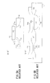
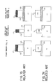
- the protection oxide film 18 is formed not only on the multilayer gate electrode structure 16F but also on the sidewall faces of each of the gate electrode 16B formed in the low-voltage operation transistor region B and the gate electrode 16C formed in the high-voltage operation transistor region C as shown in FIGS. 2A and 2B.
- the protection oxide film 18 forms bird's beaks that penetrate under the gate electrode 16B in the region B as shown circled by broken lines in FIG. 2B. Therefore, especially in a low-voltage operation transistor whose gate length is short, that is, whose gate oxide film 12B is thin, a substantial change in the thickness of the gate oxide film 12B is effected right under the gate electrode 16B, thus causing a problem that a threshold characteristic shifts from a desired value.
- the protection oxide film 18 is not formed.
- electrons retained in the amorphous silicon pattern 13A (hereinafter, also referred to as a floating gate electrode pattern 13A) are dissipated to the sidewall insulating films 16s formed by CVD and etchback in the step of FIG. 10 as shown in FIG. 3B so that information stored in the flash memory device is lost in a short period of time.
- the protection oxide film 18 that is a high-quality thermal oxide film hardly allowing a leakage current being formed on the sidewalls of the floating gate electrode pattern 13A, the electrons injected into the floating gate electrode pattern 13A are stably retained therein as shown in FIG. 3A.
- protection oxide film 18 it is essential to form the protection oxide film 18 in the semiconductor integrated circuit device including the flash memory device.
- formation of such a protection oxide film inevitably causes the problem of a change in the threshold characteristic of a MOS transistor forming a peripheral or logic circuit. Such a problem of a change in the threshold characteristic of the MOS transistor is noticeable when the MOS transistor is a high-speed transistor having a short gate length.
- FIG. 4 is a plan view of a configuration of a flash memory cell (flash memory device) having a single-layer gate electrode structure by related art.
- flash memory cell flash memory device
- FIG. 4 the same element as those of the previous drawings are referred to by the same numerals, and a description thereof will be omitted.
- a device region 11A is formed on the Si substrate 11 by a field oxide film 11F.
- One end of the above-described floating gate electrode pattern 13A is formed on the Si substrate 11 to cross the device region 11A.
- the n - -type source region 11a and the n + -type source line region 11b are formed on one side, and the n + -type drain region 11c is formed on the other side.
- n + -type diffusion region 11C is formed in the device region 11B.
- the other end of the floating gate electrode pattern 13A is formed as a coupling part 13Ac covering the diffusion region 11C.
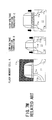
- FIG. 5A is a sectional view of the flash memory cell of FIG. 4 taken along the line X-X'.
- the tunnel oxide film 12A is formed between the source line region 11b and the drain region 11c on the Si substrate 11, and the floating gate electrode pattern 13A is formed on the tunnel oxide film 12A. Further, the n - -type source region 11a is formed outside the n + -type source line region 11b in the Si substrate 11. The sidewall insulating films 16s are formed on the sidewalls of the floating gate electrode pattern 13A.
- FIG. 5B is a sectional view of the flash memory cell of FIG. 4 taken along the line Y-Y'.
- the floating gate electrode pattern 13A continuously extends from the device region 11A to the adjacent device region 11B on the field oxide film 11F formed on the Si substrate 11.
- the coupling part 13Ac of the floating gate electrode pattern 13A is capacitive-coupled via an oxide film 12Ac to the high-density diffusion region 11C.
- the potential of the floating gate electrode pattern 13A rises so that hot electrons are injected into the floating gate electrode pattern 13A via the tunnel oxide film 12A in the device region 11A.
- an erase voltage of +15 V is applied to the source line region 11b with the drain region 11c and the high-density diffusion region 11C being grounded as shown in FIGS. 6C and 6D.
- the electrons in the floating gate electrode pattern 13A tunnel through the tunnel oxide film 12A to the source region 11a to be absorbed into a source power supply through the source line region 11b.
- the high-density diffusion region 11C serves as a control gate electrode, and unlike the conventional flash memory cell of a multilayer gate structure, it is unnecessary to form the above-described ONO insulating film 14 between the polysilicon floating gate electrode and the polysilicon control gate electrode.
- the oxide film 12Ac serves as the ONO insulating film 14. Since the oxide film 12Ac is formed on the Si substrate 11 by thermal oxidation, the oxide film 12Ac has high quality.
- FIGS. 7A through 7M are diagrams showing a production process of a semiconductor integrated circuit device including the flash memory cell of FIG. 4 in addition to the low-voltage operation transistor B and the high-voltage operation transistor C.
- the same elements as those previously described are referred to by the same numerals, and a description thereof will be omitted.
- the thermal oxide film 12C of a thickness of 5 to 50 nm is formed on the Si substrate 11 by performing thermal oxidation at temperatures ranging from 800 to 1100 °C in each of the flash memory cell region A, the low-voltage operation transistor region B, and the high-voltage operation transistor region C.
- the thermal oxide film 12C is removed from the flash memory cell region A by a patterning process using a resist pattern 15 1 .
- the resist pattern 15 1 is removed, and the tunnel oxide film 12A of a thickness of 5 to 15 nm is formed on the surface of the Si substrate 11 in the region A by performing thermal oxidation at temperatures ranging from 800 to 1100 °C.
- the thermal oxide film 12C is developed in each of the regions B and C.
- the thermal oxide film 12C is removed from the low-voltage operation transistor region B by a patterning process using a resist pattern 15 2 .
- the thermal oxide film 12B of a thickness of 3 to 10 nm is formed on the exposed Si substrate 11 in the region B by performing thermal oxidation at temperatures ranging from 800 to 1100 °C.
- the tunnel oxide film 12A is developed in the region A and the thermal oxide film 12C is developed in the region C.
- the amorphous silicon film 13 uniformly doped with P and having a thickness of 150 to 200 nm is formed on the Si substrate 11.
- patterning is performed on the amorphous silicon film 13 with a resist pattern 17 1 serving as a mask, so that the floating gate electrode pattern 13A is formed in the flash memory cell region A, a gate electrode pattern 13B is formed in the low-voltage operation transistor region B, and a gate electrode pattern 13C is formed in the high-voltage operation transistor region C.
- the surfaces of the floating gate electrode pattern 13A and the gate electrode patterns 13B and 13C are covered with the protection oxide film 18 of a thickness of 5 to 10 nm by thermal oxidation at temperatures ranging from 800 to 900 °C.
- the source region 11a is formed by performing ion implantation of P + or As + with a dose of 1 ⁇ 10 14 to 5 ⁇ 10 14 cm -2 at accelerating voltages ranging from 30 to 80 keV.
- ion implantation of As + is performed with a dose of 5 ⁇ 10 14 to 3 ⁇ 10 15 cm -2 at accelerating voltages ranging from 30 to 50 keV in the region A by using the floating gate electrode pattern 13A as a self-alignment mask.
- the n + -type source line region 11b is formed inside the source region 11a and the n + -type drain region 11c is formed on the opposite side of a channel region from the source region 11a.
- a resist pattern 17 3 covering the flash memory cell region A is formed, and the LDD regions 11d and 11e are formed in the regions B and C, respectively, by ion implantation of a p-type or n-type impurity element.
- the sidewall oxide films 16s are formed on both sidewalls of each of the floating gate electrode pattern 13A and the gate electrode patterns 13B and 13C.
- the diffusion regions 11f and 11g are formed in the regions B and C, respectively, by ion implantation of a p-type or n-type impurity element.
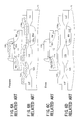
- the thermal oxide film 18 is formed as a protection insulating film to cover the single-layer gate electrode structure (the floating gate electrode pattern) 13A in the flash memory cell region A as shown in detail in FIG. 8A in the step of FIG. 7H, the same thermal oxide film 18 is also formed in the low-voltage transistor region B so as to cover the gate electrode 13B as shown in FIG. 8B.
- the low-voltage operation transistor formed in the region B is prevented from having a desired threshold characteristic.
- a more specific object of the present invention is to provide a semiconductor integrated circuit device in which formation of bird's beak right under the gate electrode of a semiconductor device formed together with a flash memory device on a substrate is effectively prevented.
- Yet another object of the present invention is to provide a method of producing such a semiconductor integrated circuit device.
- a semiconductor integrated circuit device including a substrate, a nonvolatile memory device formed in a memory cell region of the substrate and having a multilayer gate electrode structure including a tunnel insulating film covering the substrate and a floating gate electrode formed on the tunnel insulating film and having sidewall surfaces covered with a protection insulating film formed of a thermal oxide film, and a semiconductor device formed in a device region of the substrate, the semiconductor device including a gate insulating film covering the substrate and a gate electrode formed on the gate insulating film, wherein a bird's beak structure is formed of a thermal oxide film at an interface of the tunnel insulating film and the floating gate electrode, the bird's beak structure penetrating into the floating gate electrode along the interface from the sidewall faces of the floating gate electrode, and the gate insulating film is interposed between the substrate and the gate electrode to have a substantially uniform thickness.
- a semiconductor integrated circuit device including: a substrate; a nonvolatile memory device formed in a memory cell region of the substrate, the nonvolatile memory device including a first active region covered with a tunnel insulating film, a second active region formed next to the first active region and covered with an insulating film, a control gate formed of an embedded diffusion region formed in the second active region, a first gate electrode extending on the tunnel insulating film in the first active region and forming a bridge between the first and second active regions to be capacitive-coupled via the insulating film to the embedded diffusion region in the second active region, the first gate electrode having sidewall faces thereof covered with a protection insulating film formed of a thermal oxide film, and a diffusion region formed on each of sides of the first gate electrode in the first active region; and a semiconductor device formed in a device region of the substrate, the semiconductor device including a gate insulating film covering the substrate and a second gate electrode formed on the gate insulating film, wherein a
- a method of producing a semiconductor integrated circuit device including the steps of (a) forming a semiconductor structure including a tunnel insulating film covering a memory cell region of a substrate, a first silicon film covering the tunnel insulating film, an insulating film covering the first silicon film, and a gate insulating film covering a logic device region of the substrate, (b) depositing a second silicon film on the semiconductor structure formed in the step (a) so that the second silicon film covers the insulating film in the memory cell region and the gate insulating film in the logic device region, (c) forming a multilayer gate electrode structure in the memory cell region by successively patterning the second silicon film to serve as a control gate electrode, the insulating film, and the first silicon film in the memory cell region with the second silicon film being left in the logic device region, (d) forming a protection oxide film so that the protection oxide film covers the multilayer gate electrode structure in the memory cell region and the second silicon film in the logic device region, (e)
- a method of producing a semiconductor integrated circuit device including the steps of (a) forming a semiconductor structure including a tunnel insulating film covering a memory cell region of a substrate and a gate insulating film covering a logic device region of the substrate, (b) depositing a silicon film on the semiconductor structure formed in the step (a) so that the silicon film covers the tunnel insulating film in the memory cell region and the gate insulating film in the logic device region, (c) forming a first gate electrode in the memory cell region by selectively patterning the silicon film with the silicon film being left in the logic device region, (d) forming a protection oxide film so that the protection oxide film covers the first gate electrode in the memory cell region and the silicon film in the logic device region, (e) forming diffusion regions on both sides of the first gate electrode in the memory cell region by performing ion implantation of an impurity element into the substrate with the first gate electrode and the silicon film being employed as masks, (f) forming a second gate electrode in
- the protection oxide film is formed to cover the multilayer gate electrode structure or the gate electrode in the memory cell region before the gate electrode is patterned in the logic device region.
- the protection oxide film prevents the bird' beak structure from being formed as a penetration into the gate electrode in the logic device region. Therefore, the problem of a change in the threshold characteristic of the semiconductor device in the device region can be avoided.
- the diffusion regions are formed in the memory cell region by ion implantation, the device region is covered with the silicon film. By using the silicon film as a mask, a resist process may be omitted, thus simplifying the production process of the semiconductor integrated circuit device.
- FIGS. 9A through 9I are diagrams showing a production process of a semiconductor integrated circuit device according to a first embodiment of the present invention.
- the same elements as those previously described are referred to by the same numerals, and a description thereof will be omitted.
- FIGS. 1A through 1G are first performed, so that a structure corresponding to FIG. 1G is obtained in the step of FIG. 9A.
- a silicon-on-insulator (SOI) substrate may replace the Si substrate 11.
- a tunnel nitride film may replace the tunnel oxide film 12A.
- the multilayer gate electrode structure 16F is formed in the flash memory cell region A by performing patterning using the resist pattern 17A described in the step of FIG. 1H.
- no patterning is performed on the low-voltage operation transistor region B and the high-voltage operation transistor region C that are covered with the resist pattern 17A.
- the resist pattern 17A is removed, and the protection insulating film 18 is formed of a thermal oxide film to cover the multilayer gate electrode structure 16F by performing thermal oxidation at temperatures ranging from 800 to 900 °C.
- the same thermal oxide film 18 is also formed on the surface of the amorphous silicon film 16 in each of the regions B and C.
- the diffusion region 11c is formed in the flash memory cell region A by performing ion implantation of As + (or P + ) under the same conditions as in the above-described step of FIG. 1L.
- the impurity concentration may be the same on the side of the diffusion regions 11a and 11b and the side of the diffusion region 11c.
- no ion is injected into the Si substrate 11 in the regions B and C that are covered with the amorphous silicon film 16.
- a resist pattern that has an opening on the flash memory cell region A may be employed.
- step of FIG. 9D by using the resist pattern 17B previously described in the step of FIG. 1I as a mask, patterning is performed on the amorphous silicon film 16 in the regions B and C so that the gate electrodes 16B and 16C are formed in the low-voltage operation transistor region B and the high-voltage operation transistor region C, respectively.
- the LDD diffusion regions 11d are formed in the Si substrate 11 in the region B by performing ion implantation of an n-type or p-type impurity element therein.
- the LDD diffusion regions 11e are formed in the Si substrate 11 in the region C by performing ion implantation of an n-type or p-type impurity element therein.
- the diffusion regions 11d and 11e may be formed under the same ion implantation conditions in the same step.
- the sidewall insulating films 16s are formed on each of the multilayer gate electrode structure 16F and the gate electrodes 16B and 16C.
- the flash memory cell region A is covered with the resist pattern 19E.
- the diffusion regions 11f and 11g are formed in the Si substrate 11 in the regions B and C, respectively, by performing ion implantation of an n-type or p-type impurity element therein.
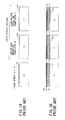
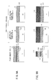
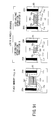
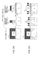
- the protection insulating film 18 when the protection insulating film 18 is formed by thermal oxidation in the step of FIG. 9C, no patterning has been performed on the amorphous silicon film 16 in the regions B and C. As a result, in the regions B and C, the thermal oxide film 18 is formed on the surface of the amorphous silicon film 16, but is prevented from being formed at an interface between the amorphous silicon film 16 and the gate oxide film 12B. Further, no such thermal oxidation is performed in any step after the patterning step of the gate electrodes 16B and 16C of FIG. 9D. Therefore, although the protection insulating film 18 is formed to cover the multilayer gate electrode structure 16F as shown in FIG. 10A, no thermal oxide film other than the gate oxide film 12B is developed on the bottom of the gate electrode 16B. Therefore, the problem of a change in the threshold characteristic of the low-voltage operation transistor can be avoided.
- bird's beaks are formed under the floating gate electrode pattern 13A with the formation of the protection insulating film 18.
- bird's beaks are far smaller in thickness and penetration distance than those formed under the floating gate electrode pattern 13A.
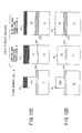
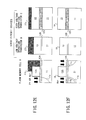
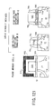
- FIGS. 12A through 12I are diagrams showing a production method of a semiconductor integrated circuit device including a flash memory device of a single-layer gate electrode structure according to a second embodiment of the present invention.
- the same elements as those previously described are referred to by the same numerals, and a description thereof will be omitted.
- steps corresponding to those of FIGS. 7A through 7D are first performed, so that a structure corresponding to that of FIG. 7E is obtained in the step of FIG. 12A.
- an SOI substrate may also replace the Si substrate 11.
- a thermal nitride oxide film may replace the tunnel oxide film 12A or the thermal oxide films 12B and 12C.
- the amorphous silicon film 13 of a thickness of 100 to 300 nm is deposited on the structure of FIG. 12A.
- the amorphous silicon film 13 may be replaced by a polysilicon film. Further, the amorphous silicon film 13 may be doped with P + .
- patterning is performed on the amorphous silicon film 13 by using a resist pattern 27 1 as a mask so that the floating gate electrode pattern 13A is formed.
- the resist pattern 27 1 covers the low-voltage operation transistor region B and the high-voltage operation transistor region C. Consequently, no patterning is performed on the amorphous silicon film 13 in the regions B and C in the step of FIG. 12C.
- the resist pattern 27 1 is removed, and the protection insulating film 18 of a thickness of 5 to 10 nm is formed of a thermal oxide film so as to cover the floating gate electrode pattern 13A in the region A by performing thermal oxidation at temperatures ranging from 800 to 900 °C.
- the thermal oxide film 18 is also formed on the surface of the amorphous silicon film 13 in the regions B and C.
- a resist pattern 27 2 corresponding to the resist pattern 17 2 in FIG. 7I is formed on the structure of FIG. 12D.
- the resist pattern 27 2 being employed as a mask, ion implantation of P + (or As + ) is performed with a dose of 1 ⁇ 10 14 to 5 ⁇ 10 14 cm -2 at accelerating voltages ranging from 30 to 80 keV so that the diffusion region 11a is formed next to the floating gate electrode pattern 13A in the flash memory cell region A.
- ion implantation of As + is performed with a dose of 1 ⁇ 10 15 to 6 ⁇ 10 15 cm -2 at accelerating voltages ranging from 30 to 80 keV so that the resistance of the diffusion region 11a is reduced.
- the resist pattern 27 2 is removed, and with the floating gate electrode pattern 13A being employed as a mask, ion implantation of As + is performed with a dose of 5 ⁇ 10 14 to 3 ⁇ 10 15 cm -2 at accelerating voltages ranging from 20 to 60 keV in the region A so that the diffusion regions 11b and 11c are formed in the Si substrate 11 in the region A.
- the step of FIG. 12E is omittable. Further, a resist pattern having an opening only on the flash memory cell region A may be formed alternatively.
- a resist pattern 27 3 is formed on the structure of FIG. 12F.
- the flash memory cell region A is covered with the resist pattern 27 3 .
- patterning is performed on the amorphous silicon film 13 with the resist pattern 27 3 being employed as a mask in the regions B and C so that the gate electrodes 13B and 13C are formed therein.
- the resist pattern 27 3 is removed and a resist pattern 27 4 covering the flash memory cell region A is formed.
- the resist pattern 27 4 being employed as a mask, an n-type or p-type impurity element is introduced into the Si substrate 11 by ion implantation so that the LDD diffusion regions 11d and 11e are formed in the regions B and C, respectively.
- the resist pattern 27 4 is removed, and a CVD oxide film 16S is deposited. Further, with the CVD oxide film 16S being protected by a resist pattern 27 5 in the flash memory cell region A, etchback is performed in the regions B and C so that the sidewall oxide films 16s are formed on the sidewalls of each of the gate electrodes 13B and 13C.
- a p-type or n-type gate electrode is also formable.
- a low-resistance silicide film of, for instance, WSi or CoSi may be formed as required on the surface of each of the gate electrodes 13B and 13C and the diffusion regions 11f and 11g by silicide processing.
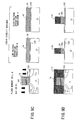
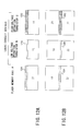
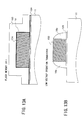
- FIGS. 13A and 13B are diagrams showing detailed configurations of the flash memory device and the low-voltage operation transistor formed according to this embodiment.
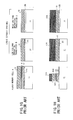
- the floating gate electrode pattern 13A has not only its sidewall faces but also its top surface uniformly covered with the protection insulating film 18 in this embodiment. Therefore, electrons accumulated in the floating gate electrode pattern 13A are stably retained even if the flash memory device is left in a hot environment for a long time.
- the amorphous silicon film 13 is not patterned in the regions B and C when the thermal oxidation step of FIG. 12D is performed. Therefore, as shown in FIGS. 13B, no bird' beaks of the thermal oxide film penetrate under the gate electrodes 13B and 13C. This stabilizes the threshold characteristic and the operation characteristic of each MOS transistor formed on the Si substrate 11 on which the flash memory device is formed as well. The improvements in the threshold characteristic and the operation characteristic are remarkable in a low-voltage operation transistor having a short gate length and a thin gate oxide film.
- the multilayer gate electrode structure 16F may also have its sidewall faces and top surface covered continuously with the protection insulating film 18 in the configuration of FIG. 9I as in that of FIG. 12I.
- a protection oxide film is formed to cover a multilayer gate electrode structure or a floating gate electrode pattern in a flash memory cell region before a gate electrode is patterned in a first or second device region.
- the protection oxide film prevents a bird' beak structure from being formed to penetrate into the gate electrode in the device region. Therefore, the problem of a change in the threshold characteristic of a semiconductor device in the device region can be avoided.
- the device region is covered with an amorphous silicon film. By using the amorphous silicon film as a mask, a resist process may be omitted, thus simplifying the production process.
Landscapes
- Engineering & Computer Science (AREA)
- Manufacturing & Machinery (AREA)
- Non-Volatile Memory (AREA)
- Semiconductor Memories (AREA)
- Metal-Oxide And Bipolar Metal-Oxide Semiconductor Integrated Circuits (AREA)
Abstract
Description
Claims (39)
- A semiconductor integrated circuit device comprising:wherein a bird's beak structure is formed of a thermal oxide film at an interface of the tunnel insulating film (12A) and the floating gate electrode (13A), the bird's beak structure penetrating into the floating gate electrode (13A) along the interface from the sidewall faces of the floating gate electrode (13A); anda substrate (11);a nonvolatile memory device formed in a memory cell region of said substrate and having a multilayer gate electrode structure (16F) comprising a tunnel insulating film (12A) covering said substrate (11) and a floating gate electrode (13A) formed on the tunnel insulating film (12A) and having sidewall surfaces covered with a protection insulating film (18) formed of a thermal oxide film; anda semiconductor device formed in a device region of said substrate (11), the semiconductor device comprising a gate insulating film (12B, 12C) covering said substrate (11) and a gate electrode (16B, 16C) formed on the gate insulating film (12B, 12C),
the gate insulating film (12B, 12C) is interposed between said substrate (11) and the gate electrode (16B, 16C) to have a substantially uniform thickness. - The semiconductor integrated circuit device as claimed in claim 1, wherein the multilayer gate electrode structure (16F) further comprises an insulating film (14A) formed on the floating gate electrode (13A) and a control gate electrode (16A) formed on the insulating film (14A).
- The semiconductor integrated circuit device as claimed in claim 2, wherein each of the gate electrode (12B, 12C) and the control gate electrode (16A) comprises a polycide or polymetal structure including a silicon film doped with an n-type or p-type dopant.
- The semiconductor integrated circuit device as claimed in claim 1, wherein the thermal oxide film forming the protection insulating film (18) connects to the bird's beak structure.
- The semiconductor integrated circuit device as claimed in claim 1, wherein the protection insulating film (18) continuously covers sidewall faces and a top surface of the multilayer gate electrode structure (16F).
- The semiconductor integrated circuit device as claimed in claim 1, wherein a silicon-on-insulator substrate is employed as said substrate.
- The semiconductor integrate circuit device as claimed in claim 1, wherein the tunnel insulating film (12A) is a tunnel oxide film.
- The semiconductor integrate circuit device as claimed in claim 1, wherein the tunnel insulating film (12A) is a tunnel nitride film.
- A semiconductor integrated circuit device comprising:a substrate (11);a nonvolatile memory device formed in a memory cell region of said substrate (11),the nonvolatile memory device comprising:a first active region (11A) covered with a tunnel insulating film (12A);a second active region (11B) formed next to the first active region (11A) and covered with an insulating film (12Ac);a control gate formed of an embedded diffusion region (11C) formed in the second active region (11B);a first gate electrode (13A) extending on the tunnel insulating film (12A) in the first active region (11A) and forming a bridge between the first and second active regions (11A, 11B) to be capacitive-coupled via the insulating film (12Ac) to the embedded diffusion region (11C) in the second active region (11B), the first gate electrode (13A) having sidewall faces thereof covered with a protection insulating film (18) formed of a thermal oxide film; anda diffusion region (11a, 11c) formed on each of sides of the first gate electrode (13A) in the first active region (11A); anda semiconductor device formed in a device region of said substrate, the semiconductor device comprising a gate insulating film (12B, 12C) covering said substrate (11) and a second gate electrode (13B, 13C) formed on the gate insulating film (12B, 12C),
wherein a bird's beak structure is formed of a thermal oxide film at an interface of the tunnel insulating film (12A) and the first gate electrode (13A), the bird's beak structure penetrating into the first gate electrode (13A) along the interface from the sidewall faces of the first gate electrode (13A); and
the gate insulating film (12B, 12C) is interposed between said substrate (11) and the second gate electrode (13B, 13C) to have a substantially uniform thickness. - The semiconductor integrated circuit device as claimed in claim 9, wherein the thermal oxide film forming the protection insulating film (18) is connected to the bird's beak structure.
- The semiconductor integrated circuit device as claimed in claim 9, wherein the protection insulating film (18) continuously covers a top surface of the first gate electrode (13A).
- The semiconductor integrated circuit device as claimed in claim 9, wherein the second gate electrode (13B, 13C) comprises a polycide or polymetal structure including a silicon film doped with an n-type or p-type dopant.
- The semiconductor integrated circuit device as claimed in claim 9, wherein a silicon-on-insulator substrate is employed as said substrate (11).
- The semiconductor integrated circuit device as claimed in claim 9, wherein the tunnel insulating film (12A) is a tunnel oxide film.
- The semiconductor integrated circuit device as claimed in claim 9, wherein the tunnel insulating film (12A) is a thermal nitride oxide film.
- A method of producing a semiconductor integrated circuit device, comprising the steps of:whereby a nonvolatile memory device is formed in the memory cell region and a semiconductor device is formed in the logic device region.(a) forming a semiconductor structure including a tunnel insulating film (12A) covering a memory cell region of a substrate (11), a first silicon film (13) covering the tunnel insulating film (12A), an insulating film (14) covering the first silicon film (13), and a gate insulating film (12C) covering a logic device region of the substrate;(b) depositing a second silicon film (16) on the semiconductor structure formed in said step (a) so that the second silicon film (16) covers the insulating film (14) in the memory cell region and the gate insulating film (12C) in the logic device region;(c) forming a multilayer gate electrode structure (16F) in the memory cell region by successively patterning the second silicon film (16) to serve as a control gate electrode (16A), the insulating film (14), and the first silicon film (13) in the memory cell region with the second silicon film (16) being left in the logic device region;(d) forming a protection oxide film (18) so that the protection oxide film (18) covers the multilayer gate electrode structure (16F) in the memory cell region and the second silicon film (16) in the logic device region;(e) forming diffusion regions (11a, 11c) in both sides of the multilayer gate electrode structure (16F) in the memory cell region by performing ion implantation of an impurity element into the substrate (11) with the multilayer gate electrode structure (16F) and the second silicon film (16) being employed as masks;(f) forming a gate electrode (16B, 16C) in the logic device region by patterning the second silicon film (16); and(g) forming diffusion regions (lid, 11e, 11f, 11g) in the logic device region by performing ion implantation with the gate electrode (16B, 16C) being employed as a mask,
- The method as claimed in claim 16,
wherein the logic device region comprises first and second device regions;said step (a) forms first and second gate insulating films (12B, 12C) in the first and second device regions, respectively, the second insulating film (12C) being thicker than the first insulating film (12B);said step (f) forms first and second gate electrodes (16B, 16C) in the first and second device regions, respectively, by patterning the second silicon film (16); andsaid step (g) forms diffusion regions (11d, 11e, 11f, 11g) in the first and second device regions by employing the first and second gate electrodes (16B, 16C) being employed as masks, respectively. - The method as claimed in claim 17,
wherein said step (b) is performed simultaneously in the memory cell region and the first and second device regions. - The method as claimed in claim 17,
wherein each of the control gate electrode (16A) and the first and second gate electrodes (16B, 16C) comprises a polycide or polymetal structure including a silicon film doped with an n-type or p-type dopant. - The method as claimed in claim 16,
wherein said step (b) is performed simultaneously in the memory cell region and the logic device region. - The method as claimed in claim 16,
wherein said step (e) is performed without using a resist mask. - The method as claimed in claim 16,
wherein said step (a) employs a tunnel oxide film as the tunnel insulating film (12A). - The method as claimed in claim 16,
wherein said step (a) employs a tunnel nitride film as the tunnel insulating film (12A). - The method as claimed in claim 16,
wherein a silicon-on-insulator substrate is employed as the substrate (11). - The method as claimed in claim 16,
wherein said step (d) forms the protection oxide film (18) by thermal oxidation so that the protection oxide film (18) is formed of a thermal oxide film. - The method as claimed in claim 16,
wherein said step (g) performs ion implantation with the memory cell region being protected by a resist mask (19D, 19E). - The method as claimed in claim 16,
wherein each of the control gate electrode (16A) and the gate electrode (16B, 16C) comprises a polycide or polymetal structure including a silicon film doped with an n-type or p-type dopant. - A method of producing a semiconductor integrated circuit device, comprising the steps of:whereby a nonvolatile memory device is formed in the memory cell region and a semiconductor device is formed in the logic device region.(a) forming a semiconductor structure comprising a tunnel insulating film (12A) covering a memory cell region of a substrate (11) and a gate insulating film (12B, 12C) covering a logic device region of the substrate;(b) depositing a silicon film (13) on the semiconductor structure formed in said step (a) so that the silicon film (13) covers the tunnel insulating film (12A) in the memory cell region and the gate insulating film (12B, 12C) in the logic device region;(c) forming a first gate electrode (13A) in the memory cell region by selectively patterning the silicon film (13) with the silicon film (13) being left in the logic device region;(d) forming a protection oxide film (18) so that the protection oxide film (18) covers the first gate electrode (13A) in the memory cell region and the silicon film (13) in the logic device region;(e) forming diffusion regions (11a, 11c) on both sides of the first gate electrode (13A) in the memory cell region by performing ion implantation of an impurity element into the substrate (11) with the first gate electrode (13A) and the silicon film (13) being employed as masks;(f) forming a second gate electrode (13B, 13C) in the logic device region by patterning the silicon film (13); and(g) forming diffusion regions (11d, 11e, 11f, 11g) in the logic device region by performing ion implantation with the second gate electrode (13B, 13C) being employed as a mask,
- The method as claimed in claim 28,
wherein the logic device region comprises first and second device regions;said step (a) forms first and second gate insulating films (12B, 12C) in the first and second device regions, respectively, the second insulating film (12C) being thicker than the first insulating film (12B);said step (f) forms third and fourth gate electrodes (13B, 13C) in the first and second device regions, respectively, by patterning the second silicon film (13); andsaid step (g) forms diffusion regions (11d, 11e, 11f, 11g) in the first and second device regions by employing the third and fourth gate electrodes (13B, 13C) being employed as masks, respectively. - The method as claimed in claim 29,
wherein said step (b) is performed simultaneously in the memory cell region and the first and second device regions. - The method as claimed in claim 29,
wherein each of the third and fourth gate electrodes (13B, 13C) comprises a polycide or polymetal structure including a silicon film doped with an n-type or p-type dopant. - The method as claimed in claim 28,
wherein said step (b) is performed simultaneously in the memory cell region and the logic device region. - The method as claimed in claim 28,
wherein said step (e) is performed without using a resist mask. - The method as claimed in claim 28,
wherein said step (a) employs a tunnel oxide film as the tunnel insulating film (12A). - The method as claimed in claim 28,
wherein said step (a) employs a tunnel nitride film as the tunnel insulating film (12A). - The method as claimed in claim 28,
wherein a silicon-on-insulator substrate is employed as the substrate (11). - The method as claimed in claim 28,
wherein said step (d) forms the protection oxide film (18) by thermal oxidation so that the protection oxide film (18) is formed of a thermal oxide film. - The method as claimed in claim 28,
wherein said step (g) performs ion implantation with the memory cell region being protected by a resist mask (274, 275). - The method as claimed in claim 28,
wherein the second gate electrode (13B, 13C) comprises a polycide or polymetal structure including a silicon film doped with an n-type or p-type dopant.
Priority Applications (1)
| Application Number | Priority Date | Filing Date | Title |
|---|---|---|---|
| EP08105801.8A EP2019430B1 (en) | 2001-07-05 | 2002-03-01 | Semiconductor non volatile memory device and method of producing the same |
Applications Claiming Priority (2)
| Application Number | Priority Date | Filing Date | Title |
|---|---|---|---|
| JP2001205188 | 2001-07-05 | ||
| JP2001205188A JP2003023114A (en) | 2001-07-05 | 2001-07-05 | Semiconductor integrated circuit device and method of manufacturing the same |
Related Child Applications (2)
| Application Number | Title | Priority Date | Filing Date |
|---|---|---|---|
| EP08105801.8A Division EP2019430B1 (en) | 2001-07-05 | 2002-03-01 | Semiconductor non volatile memory device and method of producing the same |
| EP08105801.8A Division-Into EP2019430B1 (en) | 2001-07-05 | 2002-03-01 | Semiconductor non volatile memory device and method of producing the same |
Publications (3)
| Publication Number | Publication Date |
|---|---|
| EP1274132A2 true EP1274132A2 (en) | 2003-01-08 |
| EP1274132A3 EP1274132A3 (en) | 2004-06-30 |
| EP1274132B1 EP1274132B1 (en) | 2015-10-07 |
Family
ID=19041547
Family Applications (2)
| Application Number | Title | Priority Date | Filing Date |
|---|---|---|---|
| EP02290504.6A Expired - Lifetime EP1274132B1 (en) | 2001-07-05 | 2002-03-01 | Semiconductor non volatile memory device and method of producing the same |
| EP08105801.8A Expired - Lifetime EP2019430B1 (en) | 2001-07-05 | 2002-03-01 | Semiconductor non volatile memory device and method of producing the same |
Family Applications After (1)
| Application Number | Title | Priority Date | Filing Date |
|---|---|---|---|
| EP08105801.8A Expired - Lifetime EP2019430B1 (en) | 2001-07-05 | 2002-03-01 | Semiconductor non volatile memory device and method of producing the same |
Country Status (6)
| Country | Link |
|---|---|
| US (3) | US7538376B2 (en) |
| EP (2) | EP1274132B1 (en) |
| JP (1) | JP2003023114A (en) |
| KR (1) | KR100745003B1 (en) |
| CN (2) | CN1310329C (en) |
| TW (1) | TW531880B (en) |
Cited By (6)
| Publication number | Priority date | Publication date | Assignee | Title |
|---|---|---|---|---|
| WO2006069184A1 (en) * | 2004-12-22 | 2006-06-29 | Sandisk Corporation | Eeprom array with self-aligned shallow-trench isolation |
| US7170131B2 (en) | 2002-10-09 | 2007-01-30 | Sandisk Corporation | Flash memory array with increased coupling between floating and control gates |
| US7183153B2 (en) | 2004-03-12 | 2007-02-27 | Sandisk Corporation | Method of manufacturing self aligned non-volatile memory cells |
| US7482223B2 (en) | 2004-12-22 | 2009-01-27 | Sandisk Corporation | Multi-thickness dielectric for semiconductor memory |
| US7541240B2 (en) | 2005-10-18 | 2009-06-02 | Sandisk Corporation | Integration process flow for flash devices with low gap fill aspect ratio |
| US8304310B2 (en) * | 2003-03-19 | 2012-11-06 | Fujitsu Semiconductor Limited | Manufacture method of semiconductor device |
Families Citing this family (45)
| Publication number | Priority date | Publication date | Assignee | Title |
|---|---|---|---|---|
| US6759298B2 (en) * | 2002-06-24 | 2004-07-06 | Micron Technology, Inc. | Methods of forming an array of flash field effect transistors and circuitry peripheral to such array |
| US6746921B2 (en) * | 2002-06-24 | 2004-06-08 | Micron Technology, Inc. | Method of forming an array of FLASH field effect transistors and circuitry peripheral to such array |
| KR100466194B1 (en) * | 2002-07-18 | 2005-01-13 | 주식회사 하이닉스반도체 | Method for manufacturing flash memory |
| CN100461449C (en) | 2003-10-23 | 2009-02-11 | 富士通微电子株式会社 | Semiconductor device and method for manufacturing semiconductor device |
| US7256090B2 (en) * | 2003-12-31 | 2007-08-14 | Dongbu Electronics Co., Ltd. | Method for fabricating semiconductor device |
| JP2005353984A (en) * | 2004-06-14 | 2005-12-22 | Seiko Epson Corp | Nonvolatile memory device |
| KR100673205B1 (en) * | 2004-11-24 | 2007-01-22 | 주식회사 하이닉스반도체 | Manufacturing Method of Flash Memory Device |
| JP4991134B2 (en) * | 2005-09-15 | 2012-08-01 | ルネサスエレクトロニクス株式会社 | Semiconductor device and manufacturing method thereof |
| KR100870383B1 (en) * | 2006-05-29 | 2008-11-25 | 주식회사 하이닉스반도체 | Manufacturing Method of NAND Flash Memory Device |
| KR20110008284A (en) * | 2008-04-29 | 2011-01-26 | 어플라이드 머티어리얼스, 인코포레이티드 | Photovoltaic Modules Manufactured Using Monolithic Module Assembly Technologies |
| US8228726B2 (en) * | 2008-12-14 | 2012-07-24 | Chip Memory Technology, Inc. | N-channel SONOS non-volatile memory for embedded in logic |
| CN101993037A (en) * | 2009-08-20 | 2011-03-30 | 中芯国际集成电路制造(上海)有限公司 | Method for manufacturing nanocrystalline silicon structures of semiconductor integrated circuits |
| US8399310B2 (en) | 2010-10-29 | 2013-03-19 | Freescale Semiconductor, Inc. | Non-volatile memory and logic circuit process integration |
| KR20140018081A (en) * | 2011-06-02 | 2014-02-12 | 파나소닉 주식회사 | Method of manufacturing thin film semiconductor device, method of manufacturing thin film semiconductor array substrate, method of forming crystalline silicon thin film and apparatus for forming crystalline silicon thin film |
| US8906764B2 (en) | 2012-01-04 | 2014-12-09 | Freescale Semiconductor, Inc. | Non-volatile memory (NVM) and logic integration |
| JP6179900B2 (en) * | 2012-03-30 | 2017-08-16 | パナソニックIpマネジメント株式会社 | Solar cell and manufacturing method thereof |
| US8951863B2 (en) | 2012-04-06 | 2015-02-10 | Freescale Semiconductor, Inc. | Non-volatile memory (NVM) and logic integration |
| US9087913B2 (en) | 2012-04-09 | 2015-07-21 | Freescale Semiconductor, Inc. | Integration technique using thermal oxide select gate dielectric for select gate and apartial replacement gate for logic |
| US9111865B2 (en) | 2012-10-26 | 2015-08-18 | Freescale Semiconductor, Inc. | Method of making a logic transistor and a non-volatile memory (NVM) cell |
| US9006093B2 (en) | 2013-06-27 | 2015-04-14 | Freescale Semiconductor, Inc. | Non-volatile memory (NVM) and high voltage transistor integration |
| US8877585B1 (en) * | 2013-08-16 | 2014-11-04 | Freescale Semiconductor, Inc. | Non-volatile memory (NVM) cell, high voltage transistor, and high-K and metal gate transistor integration |
| US8871598B1 (en) | 2013-07-31 | 2014-10-28 | Freescale Semiconductor, Inc. | Non-volatile memory (NVM) and high-k and metal gate integration using gate-first methodology |
| US9129996B2 (en) | 2013-07-31 | 2015-09-08 | Freescale Semiconductor, Inc. | Non-volatile memory (NVM) cell and high-K and metal gate transistor integration |
| US9082837B2 (en) | 2013-08-08 | 2015-07-14 | Freescale Semiconductor, Inc. | Nonvolatile memory bitcell with inlaid high k metal select gate |
| US9252246B2 (en) | 2013-08-21 | 2016-02-02 | Freescale Semiconductor, Inc. | Integrated split gate non-volatile memory cell and logic device |
| US9082650B2 (en) | 2013-08-21 | 2015-07-14 | Freescale Semiconductor, Inc. | Integrated split gate non-volatile memory cell and logic structure |
| US9275864B2 (en) | 2013-08-22 | 2016-03-01 | Freescale Semiconductor,Inc. | Method to form a polysilicon nanocrystal thin film storage bitcell within a high k metal gate platform technology using a gate last process to form transistor gates |
| US8932925B1 (en) | 2013-08-22 | 2015-01-13 | Freescale Semiconductor, Inc. | Split-gate non-volatile memory (NVM) cell and device structure integration |
| US8901632B1 (en) | 2013-09-30 | 2014-12-02 | Freescale Semiconductor, Inc. | Non-volatile memory (NVM) and high-K and metal gate integration using gate-last methodology |
| US9129855B2 (en) | 2013-09-30 | 2015-09-08 | Freescale Semiconductor, Inc. | Non-volatile memory (NVM) and high-k and metal gate integration using gate-first methodology |
| US9136129B2 (en) | 2013-09-30 | 2015-09-15 | Freescale Semiconductor, Inc. | Non-volatile memory (NVM) and high-k and metal gate integration using gate-last methodology |
| US9231077B2 (en) | 2014-03-03 | 2016-01-05 | Freescale Semiconductor, Inc. | Method of making a logic transistor and non-volatile memory (NVM) cell |
| US9112056B1 (en) | 2014-03-28 | 2015-08-18 | Freescale Semiconductor, Inc. | Method for forming a split-gate device |
| US9472418B2 (en) | 2014-03-28 | 2016-10-18 | Freescale Semiconductor, Inc. | Method for forming a split-gate device |
| CN103904037A (en) * | 2014-04-04 | 2014-07-02 | 武汉新芯集成电路制造有限公司 | Manufacturing method of NOR flash memory |
| US9257445B2 (en) | 2014-05-30 | 2016-02-09 | Freescale Semiconductor, Inc. | Method of making a split gate non-volatile memory (NVM) cell and a logic transistor |
| US9343314B2 (en) | 2014-05-30 | 2016-05-17 | Freescale Semiconductor, Inc. | Split gate nanocrystal memory integration |
| US9379222B2 (en) | 2014-05-30 | 2016-06-28 | Freescale Semiconductor, Inc. | Method of making a split gate non-volatile memory (NVM) cell |
| US9653164B2 (en) | 2015-03-13 | 2017-05-16 | Nxp Usa, Inc. | Method for integrating non-volatile memory cells with static random access memory cells and logic transistors |
| US9437500B1 (en) * | 2015-03-13 | 2016-09-06 | Freescale Semiconductor, Inc. | Method of forming supra low threshold devices |
| US10504912B2 (en) | 2017-07-28 | 2019-12-10 | Taiwan Semiconductor Manufacturing Co., Ltd. | Seal method to integrate non-volatile memory (NVM) into logic or bipolar CMOS DMOS (BCD) technology |
| DE102018107908B4 (en) | 2017-07-28 | 2023-01-05 | Taiwan Semiconductor Manufacturing Co., Ltd. | Method of forming an integrated circuit with a sealing layer for forming a memory cell structure in logic or BCD technology, and an integrated circuit with a dummy structure at a boundary of a device region |
| CN107946308B (en) * | 2017-11-14 | 2020-11-03 | 上海华力微电子有限公司 | Process flow method for forming control gate in storage device |
| US10825522B2 (en) * | 2018-10-29 | 2020-11-03 | United Microelectronics Corp. | Method for fabricating low and high/medium voltage transistors on substrate |
| US20250079415A1 (en) * | 2023-08-30 | 2025-03-06 | Texas Instruments Incorporated | Integrated circuit including flash memory and cmos logic circuitry |
Family Cites Families (45)
| Publication number | Priority date | Publication date | Assignee | Title |
|---|---|---|---|---|
| JPH07117527B2 (en) | 1987-12-28 | 1995-12-18 | 本田技研工業株式会社 | Oxygen concentration detector |
| US5445980A (en) * | 1988-05-10 | 1995-08-29 | Hitachi, Ltd. | Method of making a semiconductor memory device |
| JPH03206661A (en) | 1990-01-09 | 1991-09-10 | Fujitsu Ltd | Semiconductor device |
| JP2825585B2 (en) * | 1990-01-29 | 1998-11-18 | 株式会社日立製作所 | Semiconductor integrated circuit device and method of manufacturing the same |
| JP3107848B2 (en) | 1991-03-28 | 2000-11-13 | 株式会社リコー | Method for manufacturing semiconductor device including non-volatile memory |
| TW231343B (en) * | 1992-03-17 | 1994-10-01 | Hitachi Seisakusyo Kk | |
| US5592415A (en) * | 1992-07-06 | 1997-01-07 | Hitachi, Ltd. | Non-volatile semiconductor memory |
| JPH07130893A (en) * | 1993-11-05 | 1995-05-19 | Sony Corp | Semiconductor device and manufacturing method thereof |
| JP2924622B2 (en) * | 1993-12-28 | 1999-07-26 | 日本電気株式会社 | Method for manufacturing semiconductor device |
| US5404037A (en) * | 1994-03-17 | 1995-04-04 | National Semiconductor Corporation | EEPROM cell with the drain diffusion region self-aligned to the tunnel oxide region |
| US5470773A (en) * | 1994-04-25 | 1995-11-28 | Advanced Micro Devices, Inc. | Method protecting a stacked gate edge in a semiconductor device from self aligned source (SAS) etch |
| TW360980B (en) * | 1994-05-04 | 1999-06-11 | Nippon Precision Circuits | Single transistor EEPROM memory device |
| JP3532625B2 (en) * | 1994-10-06 | 2004-05-31 | 東芝マイクロエレクトロニクス株式会社 | Method for manufacturing semiconductor device |
| KR0161428B1 (en) * | 1995-08-24 | 1998-12-01 | 김광호 | Nonvolatile Semiconductor Memory Device and Manufacturing Method Thereof |
| US5847427A (en) * | 1995-12-21 | 1998-12-08 | Kabushiki Kaisha Toshiba | Non-volatile semiconductor memory device utilizing an oxidation suppressing substance to prevent the formation of bird's breaks |
| TW347567B (en) * | 1996-03-22 | 1998-12-11 | Philips Eloctronics N V | Semiconductor device and method of manufacturing a semiconductor device |
| JP3369043B2 (en) | 1996-04-30 | 2003-01-20 | 株式会社リコー | Method for manufacturing semiconductor device |
| JP3008854B2 (en) * | 1996-07-12 | 2000-02-14 | 日本電気株式会社 | Manufacturing method of nonvolatile semiconductor memory device |
| KR100224701B1 (en) * | 1996-07-16 | 1999-10-15 | 윤종용 | Nonvolatile Memory Device and Manufacturing Method |
| JPH1084051A (en) * | 1996-09-06 | 1998-03-31 | Hitachi Ltd | Semiconductor integrated circuit device and method of manufacturing the same |
| US5963808A (en) * | 1997-01-15 | 1999-10-05 | Macronix International Co., Ltd. | Method of forming an asymmetric bird's beak cell for a flash EEPROM |
| KR100234414B1 (en) * | 1997-03-05 | 1999-12-15 | 윤종용 | Non-volatile memory device and method of manufacturing the same |
| US6004829A (en) * | 1997-09-12 | 1999-12-21 | Taiwan Semiconductor Manufacturing Company | Method of increasing end point detection capability of reactive ion etching by adding pad area |
| TW437099B (en) * | 1997-09-26 | 2001-05-28 | Matsushita Electronics Corp | Non-volatile semiconductor memory device and the manufacturing method thereof |
| JPH11265987A (en) * | 1998-01-16 | 1999-09-28 | Oki Electric Ind Co Ltd | Nonvolatile memory and its manufacture |
| US6472281B2 (en) * | 1998-02-03 | 2002-10-29 | Matsushita Electronics Corporation | Method for fabricating semiconductor device using a CVD insulator film |
| JPH11274328A (en) * | 1998-03-26 | 1999-10-08 | Sanyo Electric Co Ltd | Nonvolatile semiconductor storage device and its manufacture |
| JPH11289021A (en) * | 1998-04-02 | 1999-10-19 | Hitachi Ltd | Semiconductor integrated circuit device, method of manufacturing the same, and microcomputer |
| JPH11317508A (en) * | 1998-05-06 | 1999-11-16 | Hitachi Ltd | Semiconductor integrated circuit device and method of manufacturing the same |
| EP0975020B1 (en) * | 1998-07-22 | 2009-02-11 | STMicroelectronics S.r.l. | Method for manufacturing electronic devices and corresponding devices comprising HV transistors and LV transistors with salicided junctions |
| JP2000068484A (en) * | 1998-08-19 | 2000-03-03 | Nec Corp | Nonvolatile semiconductor memory device and method of manufacturing the same, microcomputer incorporating nonvolatile semiconductor memory device, and method of manufacturing the same |
| KR100284739B1 (en) * | 1998-09-25 | 2001-05-02 | 윤종용 | Method of manufacturing non-volatile memory device |
| US6362049B1 (en) * | 1998-12-04 | 2002-03-26 | Advanced Micro Devices, Inc. | High yield performance semiconductor process flow for NAND flash memory products |
| US6406959B2 (en) * | 1999-01-04 | 2002-06-18 | Micron Technology, Inc. | Method of forming FLASH memory, method of forming FLASH memory and SRAM circuitry, and etching methods |
| US6165846A (en) * | 1999-03-02 | 2000-12-26 | Zilog, Inc. | Method of eliminating gate leakage in nitrogen annealed oxides |
| JP3892612B2 (en) * | 1999-04-09 | 2007-03-14 | 株式会社東芝 | Semiconductor device |
| JP2001007227A (en) * | 1999-06-23 | 2001-01-12 | Seiko Epson Corp | Nonvolatile semiconductor memory device |
| JP3450770B2 (en) * | 1999-11-29 | 2003-09-29 | 松下電器産業株式会社 | Method for manufacturing semiconductor device |
| US6294430B1 (en) * | 2000-01-31 | 2001-09-25 | Advanced Micro Devices, Inc. | Nitridization of the pre-ddi screen oxide |
| US6577531B2 (en) * | 2000-04-27 | 2003-06-10 | Semiconductor Energy Laboratory Co., Ltd. | Nonvolatile memory and semiconductor device |
| TW461093B (en) * | 2000-07-07 | 2001-10-21 | United Microelectronics Corp | Fabrication method for a high voltage electrical erasable programmable read only memory device |
| US6420232B1 (en) * | 2000-11-14 | 2002-07-16 | Silicon-Based Technology Corp. | Methods of fabricating a scalable split-gate flash memory device having embedded triple-sides erase cathodes |
| JP2002190534A (en) * | 2000-12-20 | 2002-07-05 | Nec Corp | Semiconductor storage device and method of manufacturing the same |
| US6436765B1 (en) * | 2001-02-09 | 2002-08-20 | United Microelectronics Corp. | Method of fabricating a trenched flash memory cell |
| CA2351025A1 (en) | 2001-06-19 | 2002-12-19 | Symagery Microsystems Inc. | Method and apparatus for controlling power consumption in an active pixel sensor array |
-
2001
- 2001-07-05 JP JP2001205188A patent/JP2003023114A/en active Pending
-
2002
- 2002-02-27 US US10/083,533 patent/US7538376B2/en not_active Expired - Fee Related
- 2002-03-01 EP EP02290504.6A patent/EP1274132B1/en not_active Expired - Lifetime
- 2002-03-01 EP EP08105801.8A patent/EP2019430B1/en not_active Expired - Lifetime
- 2002-03-06 TW TW091104168A patent/TW531880B/en not_active IP Right Cessation
- 2002-03-19 KR KR1020020014697A patent/KR100745003B1/en not_active Expired - Fee Related
- 2002-03-21 CN CNB021077452A patent/CN1310329C/en not_active Expired - Fee Related
- 2002-03-21 CN CNB2007100789224A patent/CN100459133C/en not_active Expired - Fee Related
-
2008
- 2008-10-01 US US12/285,289 patent/US7858463B2/en not_active Expired - Fee Related
-
2010
- 2010-11-18 US US12/949,046 patent/US8058131B2/en not_active Expired - Fee Related
Cited By (9)
| Publication number | Priority date | Publication date | Assignee | Title |
|---|---|---|---|---|
| US7170131B2 (en) | 2002-10-09 | 2007-01-30 | Sandisk Corporation | Flash memory array with increased coupling between floating and control gates |
| US7517756B2 (en) | 2002-10-09 | 2009-04-14 | Sandisk Corporation | Flash memory array with increased coupling between floating and control gates |
| US8304310B2 (en) * | 2003-03-19 | 2012-11-06 | Fujitsu Semiconductor Limited | Manufacture method of semiconductor device |
| US7183153B2 (en) | 2004-03-12 | 2007-02-27 | Sandisk Corporation | Method of manufacturing self aligned non-volatile memory cells |
| US7436019B2 (en) | 2004-03-12 | 2008-10-14 | Sandisk Corporation | Non-volatile memory cells shaped to increase coupling to word lines |
| WO2006069184A1 (en) * | 2004-12-22 | 2006-06-29 | Sandisk Corporation | Eeprom array with self-aligned shallow-trench isolation |
| US7202125B2 (en) | 2004-12-22 | 2007-04-10 | Sandisk Corporation | Low-voltage, multiple thin-gate oxide and low-resistance gate electrode |
| US7482223B2 (en) | 2004-12-22 | 2009-01-27 | Sandisk Corporation | Multi-thickness dielectric for semiconductor memory |
| US7541240B2 (en) | 2005-10-18 | 2009-06-02 | Sandisk Corporation | Integration process flow for flash devices with low gap fill aspect ratio |
Also Published As
| Publication number | Publication date |
|---|---|
| CN100459133C (en) | 2009-02-04 |
| US20110065248A1 (en) | 2011-03-17 |
| CN1310329C (en) | 2007-04-11 |
| KR100745003B1 (en) | 2007-08-02 |
| JP2003023114A (en) | 2003-01-24 |
| KR20030004991A (en) | 2003-01-15 |
| US20090269893A1 (en) | 2009-10-29 |
| TW531880B (en) | 2003-05-11 |
| EP2019430B1 (en) | 2018-10-17 |
| EP2019430A1 (en) | 2009-01-28 |
| EP1274132B1 (en) | 2015-10-07 |
| CN101026169A (en) | 2007-08-29 |
| EP1274132A3 (en) | 2004-06-30 |
| US20030008458A1 (en) | 2003-01-09 |
| CN1396660A (en) | 2003-02-12 |
| US8058131B2 (en) | 2011-11-15 |
| US7858463B2 (en) | 2010-12-28 |
| US7538376B2 (en) | 2009-05-26 |
Similar Documents
| Publication | Publication Date | Title |
|---|---|---|
| US7538376B2 (en) | Semiconductor integrated circuit device including a semiconductor device having a stable threshold characteristic | |
| JP4850174B2 (en) | Semiconductor device and manufacturing method thereof | |
| US8304310B2 (en) | Manufacture method of semiconductor device | |
| US7087955B2 (en) | Semiconductor device and a method of manufacturing the same | |
| US6844584B2 (en) | Memory cell, memory cell configuration and fabrication method | |
| US20020024092A1 (en) | Memory cell, memory cell arrangement and fabrication method | |
| US20050250335A1 (en) | [method of fabricating flash memory cell] | |
| US9905429B2 (en) | Semiconductor device and a manufacturing method thereof | |
| US6555869B2 (en) | Non-volatile memory device and method of manufacturing the same | |
| JP3452522B2 (en) | Method of manufacturing integrated circuit chip having embedded NVRAM array | |
| US7166887B2 (en) | EEPROM device and method of fabricating the same | |
| US20120115292A1 (en) | Method for integrating sonos non-volatile memory into a standard cmos foundry process flow | |
| KR100643629B1 (en) | Semiconductor device and manufacturing method thereof | |
| TW202520858A (en) | Erasable programmable single-poly nonvolatile memory cell | |
| KR20000039091A (en) | Flash memory device and method for manufacturing the same | |
| JPH1154637A (en) | Method of manufacturing semiconductor integrated circuit device and semiconductor integrated circuit device | |
| KR20000046745A (en) | Method for producing flash memory cell |
Legal Events
| Date | Code | Title | Description |
|---|---|---|---|
| PUAI | Public reference made under article 153(3) epc to a published international application that has entered the european phase |
Free format text: ORIGINAL CODE: 0009012 |
|
| AK | Designated contracting states |
Kind code of ref document: A2 Designated state(s): AT BE CH CY DE DK ES FI FR GB GR IE IT LI LU MC NL PT SE TR |
|
| AX | Request for extension of the european patent |
Free format text: AL;LT;LV;MK;RO;SI |
|
| PUAL | Search report despatched |
Free format text: ORIGINAL CODE: 0009013 |
|
| AK | Designated contracting states |
Kind code of ref document: A3 Designated state(s): AT BE CH CY DE DK ES FI FR GB GR IE IT LI LU MC NL PT SE TR |
|
| AX | Request for extension of the european patent |
Extension state: AL LT LV MK RO SI |
|
| 17P | Request for examination filed |
Effective date: 20040716 |
|
| AKX | Designation fees paid |
Designated state(s): DE FR IT |
|
| 17Q | First examination report despatched |
Effective date: 20080124 |
|
| RAP1 | Party data changed (applicant data changed or rights of an application transferred) |
Owner name: FUJITSU MICROELECTRONICS LIMITED |
|
| APBK | Appeal reference recorded |
Free format text: ORIGINAL CODE: EPIDOSNREFNE |
|
| APBN | Date of receipt of notice of appeal recorded |
Free format text: ORIGINAL CODE: EPIDOSNNOA2E |
|
| APBR | Date of receipt of statement of grounds of appeal recorded |
Free format text: ORIGINAL CODE: EPIDOSNNOA3E |
|
| APAF | Appeal reference modified |
Free format text: ORIGINAL CODE: EPIDOSCREFNE |
|
| RAP1 | Party data changed (applicant data changed or rights of an application transferred) |
Owner name: FUJITSU SEMICONDUCTOR LIMITED |
|
| APBT | Appeal procedure closed |
Free format text: ORIGINAL CODE: EPIDOSNNOA9E |
|
| GRAP | Despatch of communication of intention to grant a patent |
Free format text: ORIGINAL CODE: EPIDOSNIGR1 |
|
| INTG | Intention to grant announced |
Effective date: 20150529 |
|
| RIN1 | Information on inventor provided before grant (corrected) |
Inventor name: KOJI, TAKAHASHI Inventor name: HIROSHI, HASHIMOTO |
|
| GRAS | Grant fee paid |
Free format text: ORIGINAL CODE: EPIDOSNIGR3 |
|
| GRAA | (expected) grant |
Free format text: ORIGINAL CODE: 0009210 |
|
| AK | Designated contracting states |
Kind code of ref document: B1 Designated state(s): DE FR IT |
|
| REG | Reference to a national code |
Ref country code: DE Ref legal event code: R096 Ref document number: 60247528 Country of ref document: DE |
|
| PG25 | Lapsed in a contracting state [announced via postgrant information from national office to epo] |
Ref country code: IT Free format text: LAPSE BECAUSE OF FAILURE TO SUBMIT A TRANSLATION OF THE DESCRIPTION OR TO PAY THE FEE WITHIN THE PRESCRIBED TIME-LIMIT Effective date: 20151007 |
|
| REG | Reference to a national code |
Ref country code: DE Ref legal event code: R097 Ref document number: 60247528 Country of ref document: DE |
|
| PLBE | No opposition filed within time limit |
Free format text: ORIGINAL CODE: 0009261 |
|
| STAA | Information on the status of an ep patent application or granted ep patent |
Free format text: STATUS: NO OPPOSITION FILED WITHIN TIME LIMIT |
|
| 26N | No opposition filed |
Effective date: 20160708 |
|
| REG | Reference to a national code |
Ref country code: FR Ref legal event code: ST Effective date: 20161130 |
|
| PG25 | Lapsed in a contracting state [announced via postgrant information from national office to epo] |
Ref country code: FR Free format text: LAPSE BECAUSE OF NON-PAYMENT OF DUE FEES Effective date: 20160331 |
|
| PGFP | Annual fee paid to national office [announced via postgrant information from national office to epo] |
Ref country code: DE Payment date: 20190219 Year of fee payment: 18 |
|
| REG | Reference to a national code |
Ref country code: DE Ref legal event code: R119 Ref document number: 60247528 Country of ref document: DE |
|
| PG25 | Lapsed in a contracting state [announced via postgrant information from national office to epo] |
Ref country code: DE Free format text: LAPSE BECAUSE OF NON-PAYMENT OF DUE FEES Effective date: 20201001 |