EP1273961A2 - Method for producing a liquid-crystal display apparatus - Google Patents
Method for producing a liquid-crystal display apparatus Download PDFInfo
- Publication number
- EP1273961A2 EP1273961A2 EP02090225A EP02090225A EP1273961A2 EP 1273961 A2 EP1273961 A2 EP 1273961A2 EP 02090225 A EP02090225 A EP 02090225A EP 02090225 A EP02090225 A EP 02090225A EP 1273961 A2 EP1273961 A2 EP 1273961A2
- Authority
- EP
- European Patent Office
- Prior art keywords
- substrate
- layer
- insulating
- insulating substrate
- etching mask
- Prior art date
- Legal status (The legal status is an assumption and is not a legal conclusion. Google has not performed a legal analysis and makes no representation as to the accuracy of the status listed.)
- Withdrawn
Links
Images

































Classifications
-
- G—PHYSICS
- G02—OPTICS
- G02F—OPTICAL DEVICES OR ARRANGEMENTS FOR THE CONTROL OF LIGHT BY MODIFICATION OF THE OPTICAL PROPERTIES OF THE MEDIA OF THE ELEMENTS INVOLVED THEREIN; NON-LINEAR OPTICS; FREQUENCY-CHANGING OF LIGHT; OPTICAL LOGIC ELEMENTS; OPTICAL ANALOGUE/DIGITAL CONVERTERS
- G02F1/00—Devices or arrangements for the control of the intensity, colour, phase, polarisation or direction of light arriving from an independent light source, e.g. switching, gating or modulating; Non-linear optics
- G02F1/01—Devices or arrangements for the control of the intensity, colour, phase, polarisation or direction of light arriving from an independent light source, e.g. switching, gating or modulating; Non-linear optics for the control of the intensity, phase, polarisation or colour
- G02F1/13—Devices or arrangements for the control of the intensity, colour, phase, polarisation or direction of light arriving from an independent light source, e.g. switching, gating or modulating; Non-linear optics for the control of the intensity, phase, polarisation or colour based on liquid crystals, e.g. single liquid crystal display cells
-
- G—PHYSICS
- G02—OPTICS
- G02F—OPTICAL DEVICES OR ARRANGEMENTS FOR THE CONTROL OF LIGHT BY MODIFICATION OF THE OPTICAL PROPERTIES OF THE MEDIA OF THE ELEMENTS INVOLVED THEREIN; NON-LINEAR OPTICS; FREQUENCY-CHANGING OF LIGHT; OPTICAL LOGIC ELEMENTS; OPTICAL ANALOGUE/DIGITAL CONVERTERS
- G02F1/00—Devices or arrangements for the control of the intensity, colour, phase, polarisation or direction of light arriving from an independent light source, e.g. switching, gating or modulating; Non-linear optics
- G02F1/01—Devices or arrangements for the control of the intensity, colour, phase, polarisation or direction of light arriving from an independent light source, e.g. switching, gating or modulating; Non-linear optics for the control of the intensity, phase, polarisation or colour
- G02F1/13—Devices or arrangements for the control of the intensity, colour, phase, polarisation or direction of light arriving from an independent light source, e.g. switching, gating or modulating; Non-linear optics for the control of the intensity, phase, polarisation or colour based on liquid crystals, e.g. single liquid crystal display cells
- G02F1/133—Constructional arrangements; Operation of liquid crystal cells; Circuit arrangements
- G02F1/1333—Constructional arrangements; Manufacturing methods
- G02F1/1335—Structural association of cells with optical devices, e.g. polarisers or reflectors
- G02F1/133553—Reflecting elements
-
- G—PHYSICS
- G02—OPTICS
- G02F—OPTICAL DEVICES OR ARRANGEMENTS FOR THE CONTROL OF LIGHT BY MODIFICATION OF THE OPTICAL PROPERTIES OF THE MEDIA OF THE ELEMENTS INVOLVED THEREIN; NON-LINEAR OPTICS; FREQUENCY-CHANGING OF LIGHT; OPTICAL LOGIC ELEMENTS; OPTICAL ANALOGUE/DIGITAL CONVERTERS
- G02F1/00—Devices or arrangements for the control of the intensity, colour, phase, polarisation or direction of light arriving from an independent light source, e.g. switching, gating or modulating; Non-linear optics
- G02F1/01—Devices or arrangements for the control of the intensity, colour, phase, polarisation or direction of light arriving from an independent light source, e.g. switching, gating or modulating; Non-linear optics for the control of the intensity, phase, polarisation or colour
- G02F1/13—Devices or arrangements for the control of the intensity, colour, phase, polarisation or direction of light arriving from an independent light source, e.g. switching, gating or modulating; Non-linear optics for the control of the intensity, phase, polarisation or colour based on liquid crystals, e.g. single liquid crystal display cells
- G02F1/133—Constructional arrangements; Operation of liquid crystal cells; Circuit arrangements
- G02F1/136—Liquid crystal cells structurally associated with a semi-conducting layer or substrate, e.g. cells forming part of an integrated circuit
- G02F1/1362—Active matrix addressed cells
-
- G—PHYSICS
- G02—OPTICS
- G02F—OPTICAL DEVICES OR ARRANGEMENTS FOR THE CONTROL OF LIGHT BY MODIFICATION OF THE OPTICAL PROPERTIES OF THE MEDIA OF THE ELEMENTS INVOLVED THEREIN; NON-LINEAR OPTICS; FREQUENCY-CHANGING OF LIGHT; OPTICAL LOGIC ELEMENTS; OPTICAL ANALOGUE/DIGITAL CONVERTERS
- G02F1/00—Devices or arrangements for the control of the intensity, colour, phase, polarisation or direction of light arriving from an independent light source, e.g. switching, gating or modulating; Non-linear optics
- G02F1/01—Devices or arrangements for the control of the intensity, colour, phase, polarisation or direction of light arriving from an independent light source, e.g. switching, gating or modulating; Non-linear optics for the control of the intensity, phase, polarisation or colour
- G02F1/13—Devices or arrangements for the control of the intensity, colour, phase, polarisation or direction of light arriving from an independent light source, e.g. switching, gating or modulating; Non-linear optics for the control of the intensity, phase, polarisation or colour based on liquid crystals, e.g. single liquid crystal display cells
- G02F1/133—Constructional arrangements; Operation of liquid crystal cells; Circuit arrangements
- G02F1/1333—Constructional arrangements; Manufacturing methods
- G02F1/1335—Structural association of cells with optical devices, e.g. polarisers or reflectors
- G02F1/133553—Reflecting elements
- G02F1/133555—Transflectors
-
- G—PHYSICS
- G02—OPTICS
- G02F—OPTICAL DEVICES OR ARRANGEMENTS FOR THE CONTROL OF LIGHT BY MODIFICATION OF THE OPTICAL PROPERTIES OF THE MEDIA OF THE ELEMENTS INVOLVED THEREIN; NON-LINEAR OPTICS; FREQUENCY-CHANGING OF LIGHT; OPTICAL LOGIC ELEMENTS; OPTICAL ANALOGUE/DIGITAL CONVERTERS
- G02F1/00—Devices or arrangements for the control of the intensity, colour, phase, polarisation or direction of light arriving from an independent light source, e.g. switching, gating or modulating; Non-linear optics
- G02F1/01—Devices or arrangements for the control of the intensity, colour, phase, polarisation or direction of light arriving from an independent light source, e.g. switching, gating or modulating; Non-linear optics for the control of the intensity, phase, polarisation or colour
- G02F1/13—Devices or arrangements for the control of the intensity, colour, phase, polarisation or direction of light arriving from an independent light source, e.g. switching, gating or modulating; Non-linear optics for the control of the intensity, phase, polarisation or colour based on liquid crystals, e.g. single liquid crystal display cells
- G02F1/133—Constructional arrangements; Operation of liquid crystal cells; Circuit arrangements
- G02F1/136—Liquid crystal cells structurally associated with a semi-conducting layer or substrate, e.g. cells forming part of an integrated circuit
- G02F1/1362—Active matrix addressed cells
- G02F1/136227—Through-hole connection of the pixel electrode to the active element through an insulation layer
-
- G—PHYSICS
- G02—OPTICS
- G02F—OPTICAL DEVICES OR ARRANGEMENTS FOR THE CONTROL OF LIGHT BY MODIFICATION OF THE OPTICAL PROPERTIES OF THE MEDIA OF THE ELEMENTS INVOLVED THEREIN; NON-LINEAR OPTICS; FREQUENCY-CHANGING OF LIGHT; OPTICAL LOGIC ELEMENTS; OPTICAL ANALOGUE/DIGITAL CONVERTERS
- G02F1/00—Devices or arrangements for the control of the intensity, colour, phase, polarisation or direction of light arriving from an independent light source, e.g. switching, gating or modulating; Non-linear optics
- G02F1/01—Devices or arrangements for the control of the intensity, colour, phase, polarisation or direction of light arriving from an independent light source, e.g. switching, gating or modulating; Non-linear optics for the control of the intensity, phase, polarisation or colour
- G02F1/13—Devices or arrangements for the control of the intensity, colour, phase, polarisation or direction of light arriving from an independent light source, e.g. switching, gating or modulating; Non-linear optics for the control of the intensity, phase, polarisation or colour based on liquid crystals, e.g. single liquid crystal display cells
- G02F1/133—Constructional arrangements; Operation of liquid crystal cells; Circuit arrangements
- G02F1/136—Liquid crystal cells structurally associated with a semi-conducting layer or substrate, e.g. cells forming part of an integrated circuit
- G02F1/1362—Active matrix addressed cells
- G02F1/1368—Active matrix addressed cells in which the switching element is a three-electrode device
Definitions
- This invention relates to a method for producing a liquid crystal display apparatus having a reflection type panel or a half-transmitting type panel. More particularly, it relates to a method for producing a liquid crystal display apparatus having an optimum display function with simplified processes.
- a liquid crystal display apparatus employing active devices, such as thin-film transistors, features a thin thickness and a light weight, and is exploited as a high picture quality flat panel display. With the liquid crystal display apparatus, it is being contemplated to simplify the manufacturing process for realization of low production cost.
- the liquid crystal display apparatus is being used as a display unit for a mobile terminal.
- the liquid crystal display apparatus used currently is predominantly a reflection type or semi-transmitting type liquid crystal display apparatus.
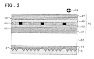
- the reflection type liquid crystal display apparatus is designed so that a reflector provided within the apparatus reflects the light incident from outside. Reflected light is used as a display light source to render unnecessary backlight as a light source (see Fig.3).
- the reflection type liquid crystal display apparatus lends itself more efficaciously to low power consumption, thinner thickness and lighter weight than the transmission type liquid crystal display apparatus.
- the semi-transmission type liquid crystal display apparatus is designed to make efficacious display even on the occasion of the weak extraneous light.
- reflection display is made by exploiting reflected light, obtained on reflection of extraneous light by a reflector, at the same time as transmission display is made by exploiting backlight transmitted through an aperture (see 4c in Fig.2) provided in a portion of the reflector.
- the basic structure of a liquid crystal display apparatus is made up by a liquid crystal of the TN (twisted nematic) system, a monolithic polarization plate system, an STN (super-twisted nematic) system, a GH (guest-host) system, a PDLC (polymer dispersion) system or a cholesteric system, a switching device, a reflector provided inside or outside the liquid crystal cell, and a transparent electrode.
- TN twisted nematic
- STN super-twisted nematic
- GH guest-host
- PDLC polymer dispersion
- cholesteric system cholesteric system
- a reflector which is used as a pixel electrode, contributes to enhancement of the intensity of light scattered in an orientation perpendicular to a display picture surface with respect to the incident light entered with a large incident angle. With this reflector, a brighter display may be produced.
- a passivation film having a roughness formed on a surface, with a reflection film, to provide a reflection surface with a roughness, an optimum reflection characteristic may be achieved.
- a typical conventional method for forming a rough surface on a reflector see for example the JP Patent Kokai JP-A-10-319422.
- a transparent electrode of ITO (indium tin oxide), used as a pixel electrode, may be formed as an uppermost layer, by layer separation from a drain layer, in order to improve the definition and aperture ratio of a display picture in a semi-transmission type liquid crystal display apparatus.
- the transparent electrode may also be formed on a surface of the reflector in order to prevent hillocks from being produced on the surface of the reflector formed of metal including Al.
- the transparent electrode may also be used in a opening provided in the reflector in the semi-transmission type liquid crystal display apparatus, adapted for transmitting the backlight therethrough, so that the transparent electrode will operate as pixel electrodes.
- the transparent electrode is also sometimes used as wiring for electrically interconnecting a drain bus line and a drain electrode isolated therefrom.
- an active matrix substrate of a TN system is made up by a scanning line (termed a gate wiring or gate bus line) and a data line (termed a drain wiring or drain bus line), extending with orthogonal angles to each other, a reflector or a transparent electrode, formed in an area defined by these wirings, and thin-film transistors (TFTs) provided in the vicinity of the intersections of the gate and drain wirings.
- the active matrix substrate also includes a channel protection film on the TFT surface for guaranteeing the performance.
- a reflector or a transparent electrode of this active matrix substrate there is formed an orientation film for orienting the liquid crystal in a preset direction.
- the liquid crystal is sealed in a space defined by the active matrix substrate and by a counter substrate carrying another orientation film, a common electrode (transparent electrode) and a color filter, to complete the liquid crystal display apparatus.
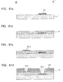
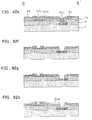
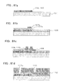
- Figs. 81a-81d and Figs. 82e-82g are cross-sectional views for schematically illustrating the processes for producing an active matrix substrate for a certain conventional reflection type liquid crystal display apparatus.
- a gate electrode layer of, for example, Cr is deposited on a transparent insulating substrate 101. Then, using a first mask, an exposed part of Cr is etched to form a gate bus line 102 and a gate electrode 103.
- a gate insulating film 105 formed of SiNx, an a-Si(amorphous silicon) film 107a and a n+ type a-Si film 107b, which is to become an ohmic contact layer, are deposited in this order, as shown in Fig.81b. Then, using a second mask, unneeded portions of the a-Si film 107a and the n+ type a-Si film 107b are selectively etched to form an island.
- source/drain electrode layer of, for example, Cr is then deposited and, using a third mask, unneeded portions of the source/drain electrode layer are selectively etched, for forming an opening in a channel area of the a-Si film 107a and a preset wiring pattern, to form a source electrode 108, which is to become a signal line, a drain electrode 109 and a drain bus line 110.
- the n + type a-Si film 107b is etched to form an ohmic contact layer.
- an organic insulating film 112 of, for example, polyimide is deposited on the entire substrate surface. Then, using a fourth mask, a contact hole 113 for exposing a portion of the source electrode 108 and a contact hole 117c for exposing a portion of the gate bus line 102 are formed.
- a portion of the organic insulating film 112 is selectively removed, using a fifth mask, and a rough portion 112b is formed, by heat treatment.
- a layer of metal such as Al is deposited on the entire substrate surface and, using a sixth photo mask, the metal layer is selectively etched to form a reflector 104b. This forms a reflector having a rough surface.
- the reflector 104b is electrically connected to the source electrode 108 through the contact hole 113.
- a transparent electrode layer of, for example, ITO(indium tin oxide) is deposited on the entire surface of the transparent insulating substrate 101, as shown in 82g. Then, using a seventh photomask, a preset portion of the transparent electrode layer is removed to form a drain terminal 117d connecting to the drain bus line 102 through the contact hole 117c and a hillock inhibiting film 152, adapted for inhibiting generation of hillocks in the reflector 104 to complete the manufacture of the active matrix substrate.
- the hillock inhibiting film may also be a transparent electrode.
- the reflector which is to become the pixel electrode and the transparent electrode are not provided on the same layer as the source/drain electrode layer, but are insulated and separated from each other by an organic insulating film. Consequently, for insulation and separation of the transparent electrode layer and the drain electrode layer, these do not have to be separated from each other in the transverse direction relative to the normal line direction of the active matrix substrate, so that these can be extremely close to or overlapped with each other.
- the black matrix for shielding the uncontrolled backlight light rays, leaking from an interstice produced when the transparent electrode layer and the drain electrode layer are separated from each other in the transverse direction can be rendered small and hence the aperture ratio can be meritoriously increased. For this reason, the transparent electrode layer and the drain electrode layer are insulated and separated from each other by an organic insulating film.
- a PR process for forming a gate bus wiring and a gate electrode namely, a PR process for forming a contact layer and a semiconductor layer, a PR process for forming a source electrode, a drain electrode and a source/bus wiring, a PR process for forming the contact hole in the organic insulating film, a PR process for forming the rough surface of the organic insulating film, a PR process for forming the reflective plate and a PR process for forming the transparent electrode.
- PR processes lead to increased production cost of the apparatus and hence to a high unit cost.
- a method for producing a liquid crystal display apparatus having a first substrate including a thin film transistor and a reflector on an insulating substrate, a second substrate having a transparent electrode and mounted facing the first substrate, and a liquid crystal layer placed between the first substrate and the second substrate, in which the method includes a first step of forming an etching mask, patterned to a preset shape, on at least one of a metal layer, an insulating layer and a semiconductor layer, formed on the insulating substrate, a second step of etching at least one of the metal layer, insulating layer and the semiconductor layer, using the etching mask, to expose a portion of the insulating substrate and to form a constituent portion of the thin film transistor and a plurality of protrusions being separated from the constituent portion, a third step of causing only the etching mask to reflow to cover exposed part of the constituent portion of the thin film transistor
- the method for producing the liquid crystal display apparatus in accordance with the present invention in case a metal layer and an insulation layer are formed in this order on the insulating substrate, it is preferred to etch the insulating layer in the second step, using the etching mask, to expose portions of the metal layer, and to stop the contact hole by the etching mask by reflow of the etching mask in the third step.
- the insulating substrate is a glass substrate and the etching liquid is HF, and the metal layer is exposed from the contact hole, there is a risk of HF permeating through the metal layer to etch the underlying glass substrate.
- the method for producing a liquid crystal display apparatus in accordance with the present invention desirably includes a sixth step following the fourth step and previous to the fifth step, with the sixth step forming another insulating layer having a rough surface on the rough surface at least formed by the protrusions and recesses. It is because this step renders it possible to adjust the rounding of the irregularities when the surface roughness of the rough surface formed by the protrusions and recesses is excessive, that is when the rough surface is square-shaped.
- a method for producing a liquid crystal display apparatus having a first substrate including a thin film transistor and a reflector on an insulating substrate, a second substrate having a transparent electrode and mounted facing the first substrate, and a liquid crystal layer placed between the first substrate and the second substrate, in which the method includes a first step of forming a metal layer on the insulating substrate, and subsequently etching the metal layer using a first etching mask to expose a portion of the insulating substrate and to form a gate electrode, a second step of causing only the etching mask to reflow to cover the exposed surface of the gate insulating electrode and near-by surface portions of the insulating substrate with the etching mask and to cover the exposed surface portions of the protrusions and near-by surface portions of the insulating substrate with the etching mask, a third step of etching the insulating substrate using the etching mask to form one or more recesses in an exposed area of the insul
- a method for producing a liquid crystal display apparatus having a first substrate including a thin film transistor and a reflector on an insulating substrate, a second substrate having a transparent electrode and mounted facing the first substrate, and a liquid crystal layer placed between the first substrate and the second substrate, in which the method includes a first step of etching the metal layer, using a first etching mask, following the formation of a metal layer on the insulating substrate, to expose a portion of the insulating substrate and to form a gate electrode, a second step of forming an insulating layer on the insulating substrate including the gate electrode and subsequently etching the insulating layer, using a second etching mask, to expose portions of the insulating substrate while forming a gate insulating film and a plurality of protrusions separated from the gate insulating films, a third step of causing only the etching mask to reflow to cover exposed portions of the gate insulating films and near-by
- a sixth step of forming a semiconductor layer on the insulating layer and of subsequently etching the semiconductor layer, using a third etching mask, to form an island above the gate electrode is preferably provided following formation of the insulating layer and prior to using the second etching mask in the second step.
- the reflector formed in the second step is directly arranged on the rough surface formed by the protrusions and recesses. It is because surface roughness of the rough surface formed by the protrusions and recesses can be prevented from being decreased.
- the reflector is of a laminated structure comprised of a lower Cr layer and an upper Al/Nd layer.
- the source electrode and the drain electrode of the laminated structure are selectively formed when the reflector is formed in the fifth step.
- a contact hole for partially exposing the Cr layer of the source electrode is formed in another insulation layer formed on the insulating layer comprised of the reflector, source electrode and the drain electrode, and in the Al/Nd layer, after forming the other insulating layer.
- a transparent electrode layer electrically connecting to the source electrode through the contact hole is selectively formed on the other insulating layer. It is because optimum electrical conductivity may be maintained between the source electrode and the transparent electrode layer, such as ITO, as hillocks are prevented from being produced on the surface of the Al/Nd layer in the reflector.
- a method for producing a liquid crystal display apparatus having a first substrate including a thin film transistor and a reflector on an insulating substrate, a second substrate having a transparent electrode and mounted facing the first substrate, and a liquid crystal layer placed between the first substrate and the second substrate, in which the method includes a first step of forming a first metal layer on the insulating substrate and subsequently etching the first metal layer, using a first etching mask, to expose a portion of the insulating substrate and to form a gate electrode, a second step of forming a first insulating layer and a semiconductor layer in this order on the insulating substrate including the gate electrode and of subsequently etching the semiconductor layer using a second etching mask to form an island above the gate electrode, a third step of forming a second metal layer on the first insulating layer including the island and of subsequently etching the second metal layer using a third etching mask to form the source electrode and the drain electrode,
- a method for producing a liquid crystal display apparatus having a first substrate including a thin film transistor and a reflector on a predominantly planar insulating substrate, a second substrate having a transparent electrode and mounted facing the first substrate, and a liquid crystal layer placed between the first substrate and the second substrate, in which the method includes a first step of etching the planar insulating substrate, using a first etching mask, to selectively form a rough surface in a preset area of the insulating substrate, and a second step of etching the metal layer, using a second etching mask, for selectively forming a gate electrode on a planar area of the insulating substrate, and for selectively forming a reflector having a rough surface overlying a rough surface of the insulating substrate in register herewith and in isolation from the gate electrode.
- a method for producing a liquid crystal display apparatus having a first substrate including a thin film transistor and a reflector on an insulating substrate, a second substrate having a transparent electrode and mounted facing the first substrate, and a liquid crystal layer placed between the first substrate and the second substrate, in which the method includes a first step of forming a first metal layer on the insulating substrate and subsequently etching the first metal layer using a first etching mask, to expose a portion of the insulating substrate, and to form a gate electrode, a plurality of protrusions separated therefrom, and a wiring isolated from the gate electrode and the protrusions, a second step of causing only the first etching mask to reflow to cover exposed surfaces of the gate electrode and the wiring and near-by surface portions of the insulating substrate with the first etching mask and to cover exposed surfaces of the protrusions and near-by surface portions of the insulating substrate with the first etching mask, a third
- a method for producing a liquid crystal display apparatus having a first substrate including a thin film transistor and a reflector on an insulating substrate, a second substrate having a transparent electrode and mounted facing the first substrate, and a liquid crystal layer placed between the first substrate and the second substrate, in which the method includes a first step of forming a first metal layer on the insulating substrate and subsequently etching the first metal layer, using a first etching mask, to expose a portion of the insulating substrate, and to form a gate electrode and a wiring separated from the gate electrode, a second step of forming a first insulating layer and a semiconductor layer in this order on the insulating substrate including the gate electrode and the wiring, and subsequently etching the semiconductor layer, using a second etching mask, to form an island above the gate electrode, a third step of etching the first insulating layer, using a third etching mask, to form a first contact hole which exposes a portion
- the etching mask is preferably a photoresist.
- the reflector has an opening in a preset area in its rough surface.
- a method for producing a liquid crystal display apparatus having a first substrate including a thin film transistor and a reflector on an insulating substrate, a second substrate having a transparent electrode and mounted facing the first substrate, and a liquid crystal layer placed between the first substrate and the second substrate includes a first step of forming an etching mask (24 of Fig.23), patterned to a preset shape, on at least one of a metal layer (3a, 25, and 26 of Fig.23), an insulating layer and a semiconductor layer, formed on the insulating substrate (1 of Fig.23), a second step (Fig.23a) of etching at least one of the metal layer, insulating layer and the semiconductor layer, using the etching mask, to expose a portion of the insulating substrate under forming a constituent portion (3a of Fig.23) of the thin film transistor and a plurality of protrusions (26 of Fig.23) being separated from the constituent portion,
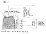
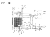
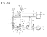
- the liquid crystal display apparatus includes a picture processing circuit, a control circuit, and a display voltage generating circuit, a drain driver(termed also as a data driver), a gate driver(termed also as a scanning line driver) and a display panel.
- the picture processing circuit executes pre-set calculations, based on the picture information, and sends the calculated picture processing signals to the control circuit.
- the control circuit performs fine position adjustment, such as alignment of the drain driver and the gate driver, based on the picture processing signals, as received, while controlling the voltage generated in a display voltage generating circuit.
- the display voltage generating circuit sends a preset voltage to each of the common terminals in the drain driver, gate driver and in the display panel, under the control from the control circuit.
- the drain driver drives the drain bus lines on the active matrix substrate in the display panel, through the drain terminal, under control from the control circuit.
- the gate driver drives the gate bus lines on the active matrix substrate in the display panel through the gate terminal under control from the control circuit.
- TCP tape carrier package
- COG chip on glass
- COF chip on flexible printed circuit board
- the display panel comprises, in the case of the semi-transmission type liquid crystal display apparatus, an orientation film 16 on the entire surface towards a transparent electrode 14 of an active matrix substrate 15 which includes a reflector 4 provided with an opening 4c.
- the display panel also comprises, on the entire surface towards the insulating substrate of the active matrix substrate 15, a phase difference plate 31, a polarization plate 32 and a backlight 33, in this order, looking from the side insulating substrate.
- a liquid crystal layer 50 is interposed between an orientation film 41 provided on an opposite side substrate 40 and an orientation film 16 provided on the active matrix substrate 15.
- the opposite side substrate 40 comprises the orientation film 41, an opposite side transparent common electrode 42, a resin protective film 43, a color filter 44, an opposite side transparent insulating substrate 45, a phase difference plate 46 and a polarization plate 47, stacked in this order from the side liquid crystal layer.
- Fig.3 showing a reflection type liquid crystal display apparatus, there is provided no backlight on the side insulating substrate of the active matrix substrate 15 provided with the reflector 4 not having the opening.
- the arrangement of the orientation film 16, liquid crystal layer 50 and the opposite side substrate 40 is not changed from that in the case of the semi-transmission type liquid crystal display apparatus.
- the active matrix substrate 15 includes a driving element for each pixel or dot in the matrix, and drives the liquid crystal by switching the driving elements.
- the active matrix substrate according the present embodiment is constructed as follows:
- an insulating substrate 1 of, for example, glass, plastics or poly-carbonate, having a rough surface 1a in a preset area
- plural gate bus lines 2 made up of, for example, Cr, Ta, Mo, Ti or Cr/Al are arranged parallel to one another.
- a gate electrode 3 is branched from each gate bus line 2.
- the insulating substrate 1 need not be transparent.
- the gate bus line 2 operates as a scanning line.
- a reflector 4 (4a and 4b) made up of, for example, Cr, Ta, Mo, Ti or Cr/Al is provided in the area of the insulating substrate 1 provided with the rough surface 1a.
- the reflector 4 is isolated from the gate bus line 2.
- the surface of the reflector 4 is rough as is the rough surface 1a of the insulating substrate 1, and extends along the rough surface 1a.
- the maximum height of the surface roughness is on the order of 2 to 3 ⁇ m, with the spacing between adjoining crests being on the order of tens of ⁇ m.
- an aperture 4c is provided in a portion of the rough surface area of the reflector 4 for transmitting the light emitted from a backlight.
- no aperture is provided in the rough surface in the reflector 4.
- the gate insulating film 5 includes a contact hole 6 for exposing a portion of the reflector 4, and has on its surface a rough surface lying on the rough surface of the reflector 4.
- an island 7 made up by a semiconductor layer 7a, formed e.g., of amorphous silicon (a-Si) or polycrystalline silicon, and a contact electrode 7b of n + type a-Si on each end of the semiconductor layer.
- a semiconductor layer 7a formed e.g., of amorphous silicon (a-Si) or polycrystalline silicon
- a contact electrode 7b of n + type a-Si on each end of the semiconductor layer.
- the drain electrode 9 is branched from the drain bus line 10(10a), which intersects the gate bus line 2 via gate insulating film 5.
- the drain bus line 10 operates as a signal line and is formed of metal, as is the drain electrode 9.
- the gate electrode 3, gate-insulating film 5, island 7, source electrode 8 and the drain electrode 9 compose a thin-film transistor (TFT) 11.
- TFT thin-film transistor
- the passivation film 12 includes a first contact hole 6 in a region corresponding to the contact hole in the gate insulating film 5, a second contact hole 13, at a preset position on the source electrode 8, for exposing the source electrode 8, and a rough surface, in an area of the rough surface of the gate insulating film 5, for extending along this rough surface of the gate insulating film.
- a transparent electrode 14 formed of, for example, ITO (indium tin oxide) or IZO (indium zinc oxide).
- the transparent electrode 14 serves to connect electrically the reflector 4 to the source electrode 8 through the first contact hole 6 and the second contact hole 13.
- the transparent electrode 1 operates, together with the reflector 4, as pixel electrodes.
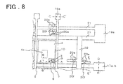
- a common terminal unit 19 At a corner of the insulating substrate 1, there are formed a common terminal unit 19, a common device unit 20 and a common bus line 21 for applying the common potential to the gate bus line 2, drain bus line 10 of the active matrix substrate 15 and to the opposite side transparent common electrode 42 of the opposite side substrate 40 of Figs.2 and 3.
- a storage capacitor may be formed between each TFT 11 and the neighboring gate bus line 2.
- a first mask is formed on a planar insulating substrate 1 of, for example, glass, by a photolithography technique.
- a rough surface 1a then is formed on the insulating substrate 1 having a flat surface, such as a glass substrate, by a photolithography technique.
- wet etching employing HF (hydrofluoric acid), sand-blasting, or dry etching, employing CF 4 or O 2 , a rough surface 1a is formed in a preset area of the insulating substrate 1.
- the resulting product is washed and the first mask is removed.
- the wet etching of the glass substrate is meritorious in that the back surface of the substrate is simultaneously etched to thereby reduce the substrate thickness.
- underlying metal layers 2a, 3a, 4a and 17a of, for example, Cr, Ti or Mo (referred to below as 'Cr'), and overlying metal layers 2b, 3b, 4b and 17b of, for example, Al (referred to below as 'Al/Nd' are deposited in this order on the entire surface of the insulating substrate 1 to form a gate electrode layer, not shown.
- the gate electrode layer is deposited, using, for example, a sputtering method, so that the total film thickness of the underlying metal Cr and the overlying metal Al/Nd will be in the order of 100 to 200 nm.
- a second mask is formed by the photolithography technique on the gate electrode layer.
- An unneeded electrode layer then is removed by dry etching or wet etching.
- the second mask then is removed. This forms the gate electrode 3, the gate bus line 2, underlying metal layers 17a and 17b of the gate terminal unit, reflector 4, an underlying metal layer 19a, a common bus line 21 for the drain and gate electrodes 20d, and 20e for the common device unit.
- the underlying metal layers 17a and 17b are connected to the gate bus line 2.
- no aperture is provided in the reflector 4
- an aperture 4c is provided in the reflector 4.
- the underlying metal layer 19a for the common terminal unit is connected to the common bus line 21 for the drain.
- the gate electrode 20d for the common device unit is connected to the common bus line 21 or to the gate bus line 2.
- the gate electrode 20e for the common device unit is separated from the common bus line 21 for the drain and from the gate bus line 2.
- the gate insulating film 5, a-Si layer 7a which is to become a semiconductor layer, and an n + type a-Si layer 7b, which is to become a contact electrode, are sequentially formed on the entire surface of the substrate provided with the gate electrode 3, gate bus line 2, underlying metal layers 17a and 17b for the gate terminal unit, reflector 4, underlying metal layer 19a for the common terminal unit, common bus line 21 for the drain and the gate electrodes 20d, and 20e for the common device unit.
- the semiconductor layer and the contact electrode form islands 7 and 20f.
- the gate insulating film 5 is formed by for example a plasma CVD method to a film thickness of the order of 300 to 500 nm.
- a-Si for example, is formed to a film having a film thickness on the order of 150 to 400 nm, by a plasma CVD method, while n + a-Si is formed to a film having a film thickness on the order of 20 to 60 nm, by a plasma CVD method.
- n + type a-Si layer 7b a substrate on which film deposition has been completed up to the a-Si layer 7a is held in a PH 3 plasma atmosphere and phosphorus(P) is diffused into the a-Si layer 7a to form an n + layer, as a surface layer, in order to form an ohmic contact to the a-Si layer 7a.
- the processing conditions for achieving this include using a plasma CVD system, supplying the PH 3 /H 2 (0.5% PH 3 ) gas at 1000 sccm at a temperature of 300°C and processing for five minutes under a pressure of 200 Pa and an RF power of 0.1W/cm 2 .
- a third mask is formed by the photolithography technique on the n + type a-Si layer 7b. Then, by e.g., dry etching, the unneeded a-Si layer 7a and unneeded n + type a-Si layer 7b are removed and the third mask then is removed. This forms the dry islands 7, 20f.
- the island 7 is formed above the gate electrode 3 adapted for driving a liquid crystal.
- the island 20f is formed above the gate electrodes 20d for the common device, the gate electrodes 20e for the common device unit, gate electrodes 20d for the common device unit and the gate electrodes 20e for the common device unit.
- metal layers 8a, 9a, 10a, 18a, 20a and 22a are deposited on the entire surface of the substrate, provided with the gate electrode 3, gate bus line 2, underlying metal layers 17a and 17b for the gate terminal unit, reflector 4, underlying metal layer 19a for the common terminal unit, common bus line 21 for the drain, gate electrodes 20d, and 20e for the common device unit, and the islands 7, and 20f, to a film thickness of 100 to 200 nm, by e.g., a sputtering method.
- a fourth mask is formed, by a photolithography technique, on the metal layers 8a, 9a, 10a, 18a, 20a and 22a. Then, unneeded metal is removed by dry etching.
- This forms a source electrode 8, a drain electrode 9, a drain bus line 10, an underlying metal 18a for the drain terminal unit, a common bus line 22 for the gate, and plural source/drain electrodes 20a for the common device unit. Part of plural source/drain electrodes 20a for the common device unit is connected to the drain bus line 10 and to the common bus line 22a for the gate.
- n + type a-Si layer 7b then is etched, using the source electrode 8a, drain electrode 9a and the fourth mask, as etching masks.
- the fourth etching mask then is removed. This forms an ohmic contact layer.
- a passivation film 12 of, for example, SiN x is formed to a film thickness of 100 to 500 nm, by the plasma CVD method, on the entire surface of the substrate provided with the gate electrode 3, gate bus line 2, underlying metal layers 17a and 17b for the gate terminal unit, reflector 4, underlying metal layer 19a for the common terminal unit, common bus line 21 for the drain, gate electrodes 20d and 20e for the common device unit, islands 7, and 20f, source electrode 8, drain electrode 9, drain bus line 10, underlying metal 18a for the drain terminal unit, common bus line 22a for the gate, and plural source/drain electrodes 20a for the common device unit.
- such a material is to be selected and used which will give a sufficiently large etching selection ratio for the a-Si a7 and the gate insulating film 5, in order to form the contact holes 6, 13 and the like in the subsequent process steps.
- a fifth mask is formed, by a photolithography technique, on the passivation film 12. Then, excess portions of the passivation film 12, gate insulating film 5 or the Al/Nd layers 2b, 4b, 17b, 19a and 21b, lying in areas which later become contact holes, are removed by, for example, dry etching, until part of the Cr layers 2a, 4a, 8a, 10a, 17a, 18a, 19a, 20a, 20d, 20e, 21a and 22a is exposed. The fifth mask then is removed. With this process, contact holes 6, 13, 17c, 18c, 19b, 20c, 21c and 22c are formed.
- the contact hole 6 exposes part of the Cr layer 4a of the reflector.
- the contact hole 13 exposes part of the source electrode (Cr layer) 8a.
- the contact hole 17c exposes part of the Cr layer 17a of the gate terminal unit.
- the contact hole 18c exposes part of the Cr layer 18a of the drain terminal unit.
- the contact hole 19b exposes part of the Cr layer 19a of the common terminal unit.
- the contact hole 21c exposes part of the Cr layer 21a for the common bus line for the drain.
- the contact hole 22c exposes part of the Cr layer 22a of the common bus line for the gate.
- Al/Nd layers 2b, 4b, 17b, 19a and 21b for the contact holes 6, 17c, 19b and part of 20c, 20e and 21r are removed is that, without this removal, the electrical conductivity of Al/Nd with the ITO which later becomes the pixels in the subsequent process is not good.
- transparent electrode layers 14, 17d, 18d, 19c, 20g and 23 of, for example, ITO are deposited, by sputtering, on the entire surface substrate provided with the passivation film 12, to a film thickness of the order of 30 to 100 nm.
- a sixth mask is formed by a photolithography technique on the transparent electrode layers 14, 17d, 18d, 19c, 20g and 23. Then, unneeded portions of the transparent electrode layers are removed by wet etching (oxalic acid, aqua regia, ferric chloride plus hydrochloric acid). The sixth mask then is removed. This forms a transparent electrode 14 which later becomes a pixel electrode, a terminal 17d of the gate terminal unit, a terminal 18d of the drain terminal unit, a terminal 19c of the common terminal unit, a wiring 20g of the common terminal unit and a wiring 23 across the common bus lines 21 and 22.
- the transparent electrode 14 electrically connects the source electrode 8 and the reflector 4 through the contact holes 6 and 13 (see Figs.7 and 9).
- the terminal 17d of the gate terminal unit, the terminal 18d of the drain terminal unit and the terminal 19c of the common terminal unit connect to the Cr layers 17a, 18a and 19a of the respective parts through contact holes 17c, 18c and 19b of the respective parts.
- the wiring 20f of the common device unit electrically connects the gate bus line 2 to the source/drain electrode 20a of the common device unit, while connecting the common bus line 22 to the gate electrode 20e of the common device unit, connecting the common bus line 21 to the source/drain electrode 20a of the common device unit and connecting the drain bus line 10 to the gate electrode 20e of the common device unit.
- the wiring 23 across the common bus lines 21, and 22 electrically connects the common bus lines 21, 22 across the contact holes 21c, and 22c.
- the transparent electrode 14 as the pixel electrode, is formed on the uppermost layer of the substrate, there is derived a merit that the electrical field can be applied directly to the liquid crystal without separation by e.g., an insulating film.
- the transparent electrode 14 is desirably provided as an uppermost layer of the substrate, even in the case of the reflection type apparatus.
- the above process may produce the active matrix substrate, constructed as shown in Fig.11.
- a reflection type or semi-transparent type active matrix substrate of optimum display performance, presenting irregularities on its reflector can be formed using only six masks, so that the manufacturing process can be simplified at least by one PR as compared to the customary manufacturing process.
- the active matrix substrate according to the second embodiment is constructed in the following manner.
- the structure of the liquid crystal display apparatus except the active matrix substrate is the same as that of the first embodiment.
- plural gate lines 2 are arranged parallel to one another. From each gate bus line 2 is branched a gate electrode 3.
- a gate electrode 3 On the planar top surface in the rough surface 1a on the insulating substrate 1, there is provided a projection member 26 formed of the same metal as the gate electrode 3, for example, Cr, Ta, Mo, Ti or Cr/Al.
- the projection member 26 serves as a basis in forming the rough surface of the reflector 4 along with the rough surface 1a of the insulating substrate 1.
- a shorting prohibiting wiring 25 adapted for preventing shorting across the reflector 4 and the gate electrode 3 and for separating the projection member 26 from the gate electrode 3.
- a gate insulating film 5 of SiN x or SiO x is formed on the insulating substrate 1, including the gate electrode 3, a shorting prohibiting wiring 25 and the projection member 26, a gate insulating film 5 of SiN x or SiO x is formed.
- the gate insulating film 5 includes contact holes 27, 28, at preset positions on the shorting prohibiting wiring 25 for exposing this shorting prohibiting wiring 25.
- the gate insulating film 5 also includes, in its area on a roughened surface formed by the rough surface 1a and the projection member 26 of the insulating substrate 1, a rough surface on this surface.
- the contact hole 27 is a hole for electrically connecting the source electrode 8 and the shorting prohibiting wiring 25.
- the contact hole 28 is a hole for electrically interconnecting the transparent electrode 14 and the shorting prohibiting wiring 25.
- an island 7 comprised of a semiconductor layer 7a and a contact electrode 7, stacked in this order.
- a source electrode 8 (8a and 8b) and a drain electrode 9(9a, and 9b), respectively.
- the source electrode 8 is electrically connected through the contact hole 27 to the shorting prohibiting wiring 25.
- the drain electrode 9 is branched from a drain bus line 10 (10a and 10b) intersecting the gate bus line 2 through the gate insulating film 5.
- the reflector 4 which is formed of the same metal as the source electrode 8 or the drain electrode 9 and which serves for separating these electrodes from each other.
- the surface of the reflector 4 also has a rough surface substantially similar to the roughened surface formed by the rough surface 1a and the projection member 26.
- the maximum height of the surface roughness is of the order of 2 to 3 ⁇ m, with the distance between neighboring crests of the projection member being of the order of tens of ⁇ m.
- an aperture 4c for transmitting a backlight are provided in an area of the rough surface of the reflector 4.
- the gate electrode 3, gate-insulating film 5, island 7, source electrode 8 and the drain electrode 9 make up a thin film transistor 11 (TFT).
- TFT 11 operates as a switching device.
- a passivation film 12 is formed on the entire surface of the substrate including the TFT 11 and the reflector 4.
- the passivation film 12 includes a contact hole 28 corresponding to the contact hole in the gate insulating film 5 and has a rough surface corresponding to the rough surface of the reflector 4.
- the transparent electrode 14 is formed in the area of the passivation film 12 presenting the rough surface.
- a gate electrode layer (Cr layer, not shown), which later becomes underlying metal layers 2a, 3a, 17a, 18a, 19a, 20d, 20e, 21a, 25 and 26, is formed on the entire surface of the insulating substrate 1 having a planar surface.
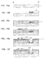
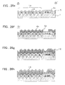
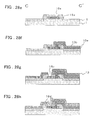
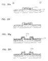
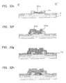
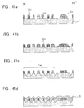
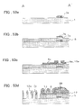
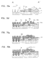
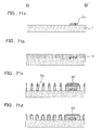
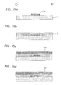
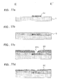
- a first mask 24 is formed on the gate electrode layer by a photolithography technique. Then, unneeded portions of the gate electrode layer are removed by for example dry etching or wet etching. This forms the gate bus line 2, gate electrode 3, underlying metal layer 17a of the gate terminal unit, underlying metal layer 18a of the drain terminal unit, underlying metal layer 19a of the common terminal unit, gate electrodes 20d, 20e for the common device unit, common bus line 21 for the drain, shorting prohibiting wiring 25 and the projection member 26. At this stage, the first mask 24 has not been removed.
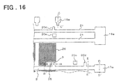
- Figs.16, 23b, 25b, 27b, 29b and 31b exposed sidewall sections of the gate bus line 2, gate electrode 3, underlying metal layer 17a of the gate terminal unit, underlying metal layer 18a of the drain terminal unit, underlying metal layer 19a of the common terminal unit, gate electrodes 20d, 20e for the common device unit, common bus line 21 for the drain, shorting prohibiting wiring 25 and the projection member 26 and near-by surface portions of the insulating substrate 1 are covered by the first mask 24, by reflow processing, which is carried out to such an extent that only the first mask 24 is melted.
- the distance between the gate electrode 3 and the shorting prohibiting wiring 25 is several ⁇ m and that between the neighboring projection members 26 is tens of ⁇ m, it is possible to make the first mask 24 continuous between the gate electrode 3 and the shorting prohibiting wiring 25 while making the first mask 24 non-continuous between the neighboring projection members 26.
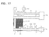
- a rough surface 1a is formed at a preset area of the insulating substrate 1 by for example wet etching employing HF (hydrofluoric acid), sandblasting or dry etching employing CF 4 or O 2 .
- the resulting product then is rinsed and the first mask removed.
- a broken line in Fig.17 indicates a step 1b of the insulating substrate. In this area, defined by the broken line in Fig.17, the surface of the insulating substrate 1 is the original flat area, with an area lying outside the surrounded area being lower in level.
- Such etching of the insulating substrate 1 in the step following the formation of for example the gate electrode 3 is meritorious in that, since HF is not interposed between e.g., the gate electrode and glass if the insulating substrate is formed of glass, it is possible to prevent peeling of e.g., the gate electrode.
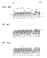
- a gate insulating film 5 of e.g., SiN x , an a-Si layer 7a, which is to become a semiconductor layer, and an n + type a-Si layer 7b, which is to become a contact electrode, are sequentially formed on the entire surface of the insulating substrate 1 including the gate bus line 2, gate electrode 3, underlying metal layer 17a of the gate terminal unit, underlying metal layer 18a of the drain terminal unit, underlying metal layer 19a of the common terminal unit, gate electrodes 20d, 20e for the common device unit, common bus line 21 for the drain, shorting prohibiting wiring 25 and the projection member 26.
- a second mask is formed on the n + type a-Si layer 7b by the photolithography technique. Then, unneeded portions of the a-Si layer 7a and the n + type a-Si layer 7b are removed, by e.g., dry etching. The second mask then is removed to form islands 7 and 20f.
- a third mask is formed on the gate insulating film 5, including the islands 7, and 20f, by the photolithography technique. Then, unneeded portions of the gate insulating film 5 of an area which later become a contact hole are removed, by e.g., dry etching, until the Cr layers 2, 18a, 20e, 21 and 25 are partially exposed. The third mask then is removed. This forms contact holes 18e, 20c, 21c and 27.
- the contact hole 18e serves for partially exposing the Cr layer 18a of the drain device unit.
- the contact hole 20c serves for partially exposing the Cr layers 2, 20a, 20e and 21 of the common device unit.
- the contact hole 21c serves for partially exposing the common bus line 21, while the contact hole 27 serves for partially exposing the shorting prohibiting wiring 25.
- underlying metal layers 4a, 8a, 9a, 10a and 22a (referred to below as 'Cr'), and overlying metal layers 4b, 8b, 9b, 10b and 22b (referred to below as 'Al/Nd'), are deposited in this order, to form a source/drain electrode layer.
- a fourth mask is formed on the source/drain electrode layer, by a photolithography technique. Then, unneeded portions of the source/drain electrode layers are removed, such as by dry etching or wet etching. This forms the reflector 4, source electrode 8, drain electrode 9, and drain bus line 10, source/drain electrodes 20a, 20b for the common device unit and the common bus line 22 for the gate.
- the reflector 4 is or is not provided with an aperture, respectively.
- the reflector 4 is connected to the source electrode 8, while the source electrode 8 is connected through the contact hole 27 to the shorting prohibiting wiring 25.
- the source/drain electrodes 20a, and 20b for the common device unit are connected through the contact hole 20c to the gate bus line 2, common bus line 21 for the drain or to the gate electrode 20e of the common device unit.
- the common bus line 22 for the gate is connected through the contact hole 21c to the common bus line 21 for the drain.
- the n + type a-Si layer 7b is etched.
- the fourth mask then is removed. This forms an ohmic contact layer.
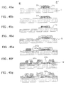
- a passivation film 12 is formed, such as by plasma CVD method, on the entire surface of the gate insulating film 5, including the source electrode 8, drain electrode 9, drain bus line 10, source/drain electrodes 20a, and 20b for the common device unit and the common bus line 22 for the gate and on the reflector 4.
- a fifth mask is formed on the passivation film 12 by a photolithography technique. Then, unneeded portions of the passivation film 12 or the gate insulating film 5 in an area which later becomes the contact hole are removed, such as by dry etching, until the Cr layers 17a, 18a, 19a and 25 are partially exposed. The fifth mask then is removed. This forms the contact holes 17c, 18c, 19b and 28.
- the contact hole 17c serves for partially exposing the Cr layer 17a of the gate terminal unit.
- the contact hole 18c serves for partially exposing the Cr layer 18 of the drain terminal unit in an area other than the contact hole 18e.
- the contact hole 19b serves for partially exposing the Cr layer 19a of the common terminal unit, while the contact hole 28 serves for partially exposing the shorting prohibiting wiring 25 in an area other than the contact hole 27.
- transparent electrode layers 14, 17d, 18d and 19c of, for example, ITO are deposited, such as by sputtering, on the entire surface of the substrate, including the passivation film 12.
- a sixth mask is finally formed, such as by a photolithography technique, on the transparent electrode layers 14, 17d, 18d and 19c.
- An excess portion of the transparent electrode layers is then removed such as by wet etching. This forms the transparent electrode 14, which later becomes the pixel electrode, the terminal 17d of the gate terminal unit, terminal 18d of the drain terminal unit and the terminal 19c of the common terminal portion.
- the transparent electrode 14 is electrically connected to the shorting prohibiting wiring 25 through contact hole 28.
- the terminal 17d of the gate terminal unit, the terminal 18d of the drain terminal unit and the terminal 19c of the common terminal unit are connected to the Cr layers 17a, 18a and 19a of the respective portions through the contact holes 17c, 18c and 19c of the respective portions.
- a reflection or semi-transmission type active matrix substrate with an optimum display function, having a reflector presenting a rough surface, may be produced, using only six masks, thus achieving a process simplified by at least one PR step as compared to the conventional manufacturing method.
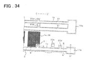
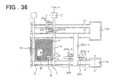
- the active matrix substrate of the third embodiment is constructed as follows. It is noted that the structure of the liquid crystal display apparatus except the active matrix substrate is the same as that of the first embodiment.
- plural gate lines 2 are arranged parallel to one another. From each gate bus line 2 is branched a gate electrode 3. On the planar top surface in the rough surface 1a on the insulating substrate 1, there are provided plural projection members 26 formed of the same metal as that of the gate electrode 3, for example, Cr, Ta, Mo, Ti or Cr/Al. The projection member 26 serves as a basis in forming the rough surface of the reflector 4 along with the rough surface 1a of the insulating substrate 1.
- a gate insulating film 5 of SiNx or SiOx is formed on the insulating substrate 1, including the gate electrode 3 and the projection member 26, a gate insulating film 5 of SiNx or SiOx is formed.
- the gate insulating film 5 also includes, in an area of the surface lying on the rough surface formed by the rough surface 1a and the projection member 26 of the insulating substrate 1, a rough surface.
- an island 7 comprised of a semiconductor layer 7a and a contact electrode 7b, stacked in this order.
- the reflector 4 (4a and 4b) is formed, without separation, in the same layer as the source electrode 8, in an area on the gate insulating film 5 overlying the roughened surface formed by the rough surface 1a of the insulating substrate 1 and the projection member 26.
- the surface of the reflector 4 presents a rough surface substantially similar to the roughened surface formed by the rough surface 1a of the insulating substrate 1 and the projection member 26, with the maximum height of the surface roughness being on the order of two to three ⁇ m, with the separation between the crests of the neighboring projection member 26 being tens of ⁇ m.
- the semi-transmission type liquid crystal display apparatus there is formed aperture 4c in a portion of the area of the rough surface in the reflector 4 for transmitting the light rays of the backlight.
- no aperture is provided in the area of the rough surface of the reflector 4.
- the drain electrode 9 is branched from the drain bus lines 10 (10a and 10b) intersecting the gate bus line 2 via gate insulating film 5.
- the gate electrode 3, gate-insulating film 5, island 7, source electrode 8 and the drain electrode 9 constitute a thin-film transistor (TFT) 11.
- TFT thin-film transistor
- a transparent electrode 14 which connects to the reflector 4 through the first contact hole 6.
- the transparent electrode 14 operates, together with the reflector 4, as pixel electrodes.
- a gate electrode layer (Cr layer, not shown), which later becomes underlying metal layers 2a, 3a, 17a, 18a, 19a, 20d, 20e and 21a, is formed on the entire surface of the insulating substrate 1 having a planar surface.
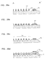
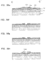
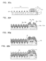
- a first mask 24 is formed on the gate electrode layer by a photolithography technique. Then, unneeded portions of the gate electrode layer are removed by for example dry etching or wet etching. This forms the gate bus line 2, gate electrode 3, underlying metal layer 17a of the gate terminal unit, underlying metal layer 19a for the common terminal unit, gate electrodes 20d, 20e for the common device unit and the common bus line 21 for the drain. At this stage, the first mask 24 has not been removed.
- exposed sidewall sections of the gate bus line 2, gate electrode 3, underlying metal layer 17a of the gate terminal unit, underlying metal layer 19a of the common terminal unit, gate electrodes 20d, and 20e for the common device unit and the common bus line 21 for the drain, and near-by surface portions of the insulating substrate 1, are covered by the first mask 24, by reflow processing, which is carried out to such an extent that only the first mask 24 is melted.
- the rough surface 1a is formed at a preset area of the insulating substrate 1 by for example wet etching employing HF (hydrofluoric acid), sandblasting or dry etching employing CF 4 or O 2 .
- the resulting product then is rinsed and the first mask removed.
- the broken line in Fig.34 indicates a step 1b of the insulating substrate. In this area, defined by the broken line in the drawing, the surface of the insulating substrate 1 is the original flat area, with an area lying outside the surrounded area being lower in level.
- a gate insulating film 5 of e.g., SiNx, an a-Si layer 7a, which is to become a semiconductor layer and an n + type a-Si layer 7b which is to become a contact electrode, are sequentially formed on the entire surface of the insulating substrate 1 including the gate bus line 2, gate electrode 3, underlying metal layer 17a of the gate terminal unit, underlying metal layer 19a of the common terminal unit, gate electrodes 20d, and 20e for the common device unit and the common bus line 21 for the drain.
- a second mask is formed on the n + type a-Si layer 7b by the photolithography technique. Then, unneeded portions of the a-Si layer 7a and the n + type a-Si layer 7b are removed, by e.g., dry etching. The second mask then is removed to form islands 7 and 20f.
- underlying metal layers 4a, 8a, and 9a. 10a and 22a (referred to below as 'Cr'), and metal overlying layers 4b, 8b, 9b, 10b and 22b of, for example, Al (referred to below as 'Al/Nd') are deposited in this order on the entire surface of the insulating substrate to form a source/drain electrode layer, not shown.
- a third mask is formed by the photolithography technique on a source/drain electrode layer. Then, unneeded portions of the source/drain electrode layer are removed by for example dry etching or wet etching. This forms the reflector 4, source electrode 8, drain electrode 9, drain bus line 10, source/drain electrode layers 20a, 20b for the common device unit, and the common bus line 22 for the gate.
- the reflector 4 In the case of the reflection type liquid crystal display apparatus, no aperture is provided in the rough surface in the reflector 4. In the case of the semi-transmission type liquid crystal display apparatus, there is formed an aperture 4c.
- the reflector 4 is formed on the same layer with the source electrode 8 and is continuous to the source electrode 8.
- the n + type a-Si layer 7b is etched.
- the third mask then is removed to form an ohmic contact layer.
- a passivation film 12 is formed, by e.g., the plasma CVD method, on the entire surface of the gate insulating film 5, inclusive of the reflector 4, source electrode 8, drain electrode 9, drain bus line 10, source/drain electrodes 20a, 20b for the common device part, and the common bus line 22 for the gate.
- a fourth mask is formed on the passivation film 12 by the photolithography technique. Then, unneeded portions of the passivation film 12, gate insulating film 5 or the Al/Nd layers 2b, 4b, 17b, 19a, 21a, lying in an area which later becomes the contact hole, are removed, such as by dry etching, until the Cr layers 2a, 4a, 10a, 17a, 18a, 19a, 20a, 20d, 20e, 21a and 22a are partially exposed. The fourth mask then is removed. This forms contact holes 6, 17c, 18c, 19b, 20c, 21c and 22c.
- the contact holes 6, 17c, 18c, 19b, 20c, 21c and 22c are those for partially exposing the Cr layer 4a of the reflector, the Cr layer 17a of the gate terminal unit, the Cr layer 18a of the drain terminal unit, the Cr layer 19a of the common terminal unit, the Cr layers 2a, 20a, 20d, 20e, 21a and 22a of the common device unit, the Cr layer 21a of the common bus line for the drain and those for partially exposing the Cr layer 22a of the common bus line Cr for the gate, respectively.
- the transparent electrode layers 14, 17d, 18d, 19c, 20g and 23 of ITO or the like are deposited, such as by sputtering method.
- a fifth mask is formed on the transparent electrode layers 14, 17d, 18d, 19c, 20g and 23, such as by the photolithography technique. Then, unneeded portions of the transparent electrode layers are removed; such as by wet etching. The fifth mask then is removed. This forms the transparent electrode 14, as pixel electrodes, terminal 17d of the gate terminal unit, terminal 18d of the drain terminal unit, terminal 19c of the common terminal unit, wiring 20g of the common device unit and the wiring 23 across the common bus lines 21 and 22.
- the transparent electrode 14 electrically connects to the Cr layer 4a of the reflector through the contact hole 6.
- the terminal 17d of the gate terminal unit, the terminal 18d of the drain terminal unit and the terminal 19c of the common terminal unit connect to the Cr layers 17a, 18a and 19a of the respective units, respectively, through the contact holes 17c, 18c and 19b of the respective units, respectively.
- the wiring 20f of the common device unit electrically connects the gate bus line 2 to the source/drain electrode 20a of the common device unit, while electrically connecting the common bus line 22 to the gate electrode 20e of the common device unit, electrically connecting the common bus 21 to the source/drain electrode 20a of the common device unit and electrically connecting the drain bus line 10 to the gate electrode 20e of the common device unit.
- the wiring 23 across the common bus lines 21 and 22 electrically interconnects the common bus lines 21 and 22 through contact holes 21c and 22c.
- the above process renders it possible to prepare the active matrix substrate having the structure shown in Fig.38.
- the method for producing the active matrix substrate according to the third embodiment, described above it is possible to produce a reflection or semi-transmitting type active matrix substrate, having a reflector presenting a rough surface, and which exhibits optimum display performance, using only five masks, thus simplifying the production method by at least two PRs as compared to the conventional production method.
- the active matrix substrate according to the fourth embodiment is constructed as follows. It is noted that the structure of the liquid crystal display apparatus except the active matrix substrate is the same as that of the first embodiment.
- plural gate lines 2 are arranged parallel to one another. From each gate bus line 2 is branched a gate electrode 3.
- a gate insulating film 5 of, for example, SiN x is formed on the insulating substrate 1 including the gate electrode 3.
- plural projection members 5a formed of the same metal as that of the gate insulating film, for example, SiNx.
- Projection members 5a serve as a basis in forming the rough surface of the reflector 4 along with the rough surface 1a of the insulating substrate 1.
- plural projection members of the same metal as that of the gate electrode 3, such as Cr may be provided between the top planar surfaces of the rough surface 1a of the insulating substrate 1 and the projection members 5a as in the second and third embodiment (refer to projection members 26 of Figs.23 and 39).
- an island 7 comprised of a semiconductor layer 7a and a contact electrode 7b, laminated in this order.
- the drain electrode 9 is branched from the drain bus line 10 (10a intersecting the gate bus line 2 via gate insulating film 5.
- the gate electrode 3, gate-insulating film 5, island 7, source electrode 8 and the drain electrode 9 constitute a thin-film transistor (TFT) 11.
- TFT thin-film transistor
- the passivation film 12 includes contact holes 6, 13, in preset areas of the source electrode 8, for exposing its Cr layer 8a.
- the contact hole 6 serves for electrically interconnecting the source electrode 8a and the reflector 4b, while the contact hole 6 serves for electrically interconnecting the source electrode 8a and the transparent electrode 14.
- a projection member 12a formed of the same material as that of the passivation film 12, for example SiNx.
- the reflector 4(4b) is formed in an area from the roughened surface formed by the rough surface 1a of the insulating substrate 1 and the projection members 5a and 12a, or projection members by the Cr layer, up to an area overlying the passivation film 12 in turn overlying the TFT 11.
- the reflector 4b overlying the roughened surface formed by the rough surface 1a of the insulating substrate 1 and by the projection members 5a, 12a, occasionally the projection members by the Cr layer, and the reflector 4b overlying the TFT 11, are formed by the same process and are electrically conducting to each other.
- the surface of the reflector 4 presents a rough surface lying on the roughened surface formed by the rough surface 1a of the insulating substrate 1 and by the projection members 5a, 12a, with the rough surface being of substantially the same shape as the roughened surface.
- the maximum height of the surface roughness is on the order of 2 to 3 ⁇ m, with the spacing between adjoining crests being on the order of tens of ⁇ m.
- no aperture is provided in the rough surface in the reflector 4.
- a transparent electrode 14 which transparent electrode 14 is electrically connected to the source electrode 8 through the contact hole 6.
- the transparent electrode 14 operates as pixel electrodes in conjunction with the reflector 4.
- ITO as the material of the transparent electrode 14 is effective to prevent hillocks from being produced by Al.
- the transparent electrode 14 (ITO) is not optimum in electrical conductivity to the reflector 4 (Al/Nd) and hence is supplied with power predominantly from the source electrode 8 (Cr).
- a gate electrode layer (Cr layer, not shown), which is to become the underlying metal layers 2a, 3a, 17a, 19a, 20d, 20e and 21a, is formed on the entire surface of the insulating substrate 1 having a planar surface.
- a first mask is formed on the gate electrode layer by the photolithography technique. Then, unneeded portions of the gate electrode layer are removed by for example dry etching or wet etching. The first mask then is removed. This sequentially forms the gate bus line 2, gate electrode 3, underlying metal layer 17a for the gate terminal unit, underlying metal layer 19a for the common terminal unit, gate electrodes 20d, 20e for the common device unit, and the common bus line 21 for the drain.
- the gate insulating film 5 of, for example, SiNx, the a-Si layer 7a, which becomes the semiconductor layer, and the n + type a-Si layer 7b, which becomes he contact electrode, are sequentially formed on the entire substrate surface comprising the gate bus line 2, gate electrode 3, underlying metal layer 17a for the gate terminal unit, underlying metal layer 19a for the common terminal unit, gate electrodes 20d, and 20e for the common device unit, and the common bus line 21 for the drain.
- a second mask is formed by the photolithography technique on the n + type a-Si layer 7b. Then, unneeded portions of the a-Si layer 7a and the n + type a-Si layer 7b are removed, such as by dry etching, and subsequently the second mask is removed. This forms islands 7 and 20f.
- a source/drain electrode layer not shown, comprised of metal layers 4a, 8a, 9a, 10a and 22a of, for example, Cr (referred to below as 'Cr'), is formed on the entire substrate surface.
- a third mask is formed on the source/drain electrode layer by the photolithography technique. Then, unneeded portions of the source/drain electrode layer are removed by for example dry etching or wet etching. This forms the source electrode 8, drain electrode 9, and drain bus line 10, source/drain electrodes 20a and 20b for the common device unit and the common bus line 22 for the gate.
- the n + type a-Si layer 7b is etched and subsequently the third mask is removed to form an ohmic contact layer.
- the passivation film 12 is formed, by the plasma CVD method, on the entire surface of the gate insulating film 5, including the source electrode 8, drain electrode 9, drain bus line 10, source/drain electrodes 20a and 20b for the common device unit and the common bus line 22 for the gate.
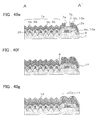
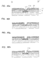
- a fourth mask 29 is formed on the passivation film 12, by the photolithography technique. Then, excess portions of the passivation film 12 or the gate insulating film 5, lying in an area which later becomes the contact hole, are removed by e.g., dry etching, until the insulating substrate 1 or Cr layers 2a, 8a, 10a, 17a, 18a, 19a, 20a, 20d, 20e, 21a and 22a are partially exposed. This forms contact holes 6, 13, 17c, 18c, 19b, 20c, 21c and 22c and projection members 5a and 12a. At this stage, the fourth mask 29 has not been removed.
- the contact hole 6 partially exposes part of the source electrode 8a.
- the contact hole 13 exposes part of the source electrode 8a.
- the contact hole 17c partially exposes part of the Cr layer 17a of the gate terminal unit.
- the contact hole 18c partially exposes part of the Cr layer 18a of the drain terminal unit.
- the contact hole 19b partially exposes part of the Cr layer 19a of the common terminal unit.
- the contact hole 20c partially exposes part of the Cr layers 2a, 20a, 20d, 20e, 21a and 22a of the common device unit.
- the contact hole 21c partially exposes part of the Cr layer 21a for the common bus line for the drain.
- the contact hole 22c partially exposes part of the Cr layer 22a of the common bus line for the gate.
- exposed sidewall sections of the gate insulating film 5, passivation film 12 and the projection members 5a, 12a and near-by surface portions of the insulating substrate 1 are covered by the fourth mask 29, by reflow processing, which is carried out to such an extent that only the fourth mask 29 is melted.
- the contact holes 6, 13, 17c, 18c, 19b, 20c, 21c and 22c as well as the exposed surface portions of the Cr layers 2a, 8a, 10a, 17a, 18a, 19a, 20a, 20d, 20e, 21a, and 22a are closed by the fourth mask 29.
- the diameter of the contact hole including the surface of the Cr layer is on the order of several ⁇ m and the interval between the neighboring projection members 5a and 12a is tens of ⁇ m, it is possible to cover the surface of each contact hole including the surface of the Cr layer with the fourth mask 29 in such a manner that the fourth mask 29 is non-continuous between the neighboring projection members 5a and 12a. In this manner, the exposed surface not covered by the fourth mask 29 may be only the portion of the insulating substrate 1 between the respective projection members 5a and 12a.
- a rough surface 1a then is formed in a preset area of the insulating substrate 1 by wet etching, employing HF (hydrofluoric acid), sandblasting, or dry etching, employing CF 4 or O 2 , a rough surface 1a is formed.
- HF hydrofluoric acid
- sandblasting sandblasting
- dry etching employing CF 4 or O 2
- the resulting product is washed and the first mask is removed.
- a layer of a reflector formed by a metal layer 4b of, for example, Al/Nd (referred to below as 'Al/Nd'), is formed on the entire surface of the substrate including the passivation film 12.
- a fifth mask is formed, by the photolithography technique, on the layer of the reflector. Then, unneeded portions of the layer of the reflector are removed by for example dry etching or wet etching. The fifth mask then is removed. This forms the reflector 4b.
- the reflector 4 connects to the source electrode 8 through the contact hole 6. Since the reflector (Al/Nd) 4 is of a material different than the source electrode (Cr) 8, the layer of the reflector can be selectively etched, based on the difference in the selection ratio, so that the Cr layers 2a, 8a, 10a, 17a, 18a, 19a, 20a, 20d, 20e, 21a and 22a can be exposed from the contact holes 13, 17c, 18c, 19b, 20c, 21c, 22c. On the other hand, the reflector 4b, above the roughened surface formed by the rough surface 1a and the projection members 5a and 12a, is electrically connected to the reflector 4b above the TFT 11.
- the transparent electrode layers 14, 17d, 18d, 19c, 20g and 23 of, for example, ITO are deposited by for example sputtering on the entire substrate surface which includes the passivation film 12.
- a sixth mask is formed, by the photolithography technique, on the transparent electrode layers 14, 17d, 18d, 19c, 20g and 23. Then, redundant portions of the transparent electrode layers are removed by for example wet etching. The sixth mask then is removed. This forms a transparent electrode 14 which later becomes pixel electrodes, a terminal 17d of the gate terminal unit, a terminal 18d of the drain terminal unit, a terminal 19c of the common terminal unit, a wiring 20g of the common terminal unit and a wiring 23 across the common bus lines 21 and 22.
- the transparent electrode 14 electrically connects to the source electrode 8a through the contact hole 13.
- the terminal 17d of the gate terminal unit, the terminal 18d of the drain terminal unit and the terminal 19c of the common terminal unit connect to the Cr layers 17a, 18a and 19a of the respective units through contact holes 17c, 18c and 19b of the respective units.
- the wiring 20f of the common device unit electrically connects the gate bus line 2 to the source/drain electrode 20a of the common device unit, while connecting the common bus line 22 to the gate electrode 20e of the common device unit, connecting the common bus line 21 to the source/drain electrode 20a of the common device unit and connecting the drain bus line 10 to the gate electrode 20e of the common device unit.
- the wiring 23 across the common bus lines 21 and 22 electrically connects the common bus lines 21 and 22 across the contact holes 21c and 22c.
- a reflection or semi-transmission type active matrix substrate with an optimum display function, having a reflector presenting a rough surface, may be produced, using only six masks, thus achieving a process simplified by at least one PR step as compared to the conventional manufacturing method.
- the active matrix substrate according to the fifth embodiment is constructed as follows. It is noted that the structure of the liquid crystal display apparatus except the active matrix substrate is the same as that of the first embodiment.
- plural gate lines 2 are arranged parallel to one another. From each gate bus line 2 is branched a gate electrode 3.
- a gate insulating film 5 formed of, for example, SiNx.
- projection members 5a formed of the same metal as the gate insulating film 5, such as SiN x .
- the projection members 5a serve as the basis in forming the rough surface of a reflector 4 along with the rough surface 1a of the insulating substrate 1.
- a shorting prohibiting wiring 25 for preventing shorting across the reflector 4 and the gate electrode 3 and for separating the projection members 5a from the gate electrode 3.
- a gate insulating film 5 of for example SiNx is formed on the insulating substrate 1, including the gate electrode 3 and the shorting prohibiting wiring 25, a gate insulating film 5 of for example SiNx is formed.
- the gate insulating film 5 includes contact holes 27 and 28, at preset positions on the shorting prohibiting wiring 25 for exposing this shorting prohibiting wiring 25.
- the contact hole 27 is a hole for electrically connecting the source electrode 8 and the shorting prohibiting wiring 25.
- the contact hole 28 is a hole for electrically interconnecting the transparent electrode 14 and the shorting prohibiting wiring 25.
- an island 7 comprised of a semiconductor layer 7a and a contact electrode 7b, laminated in this order.
- a source electrode 8 (8a and 8b) and a drain electrode 9(9a, 9b), respectively.
- the source electrode 8 is electrically connected through the contact hole 27 to the shorting prohibiting wiring 25.
- the reflector 4 (4a and 4b) is formed, without separation in the same layer as the source electrode 8, in an area overlying the roughened surface formed by the rough surface 1a of the insulating substrate 1 and the projection members 5a.
- the surface of the reflector 4 presents a rough surface substantially similar to the roughened surface formed by the rough surface 1a of the insulating substrate 1 and the projection member 26, with the maximum height of the surface roughness being on the order of two to three ⁇ m, with the separation between the crests of the neighboring projection member 26 being tens of ⁇ m.
- an aperture 4c in a portion of the area of the rough surface in the reflector 4 for transmitting the backlight.
- no aperture 4c is provided in the area of the rough surface of the reflector 4.
- the drain electrode 9 is branched from the drain bus line 10 (10a, 10b) intersecting the gate bus line 2 through the gate insulating film 5.
- the gate electrode 3, gate-insulating film 5, island 7, source electrode 8 and the drain electrode 9 constitute a thin-film transistor (TFT) 11.
- TFT thin-film transistor
- the passivation film 12 includes a first contact hole 28 corresponding to the contact hole 28 in the gate insulating film 5 for exposing the shorting prohibiting wiring 25.
- the contact hole 28 electrically connects the shorting prohibiting wiring 25 to the transparent electrode 14.
- the transparent electrode 14 operates as a pixel electrode along with the reflector 4.
- a gate electrode layer (Cr layer, not shown), which is to become the underlying metal layers 2a, 3a, 17a, 18a, 19a, 20d, 20e, 21a and 25, is formed on the entire surface of the insulating substrate 1 having a planar surface.
- a first mask is formed on the gate electrode layer by the photolithography technique. Then, unneeded portions of the gate electrode layer are removed by for example dry etching or wet etching. The first mask then is removed. This sequentially forms the gate bus line 2, gate electrode 3, underlying metal layer 17a for the gate terminal unit, underlying metal layer 19a for the common terminal unit, gate electrodes 20d, 20e for the common device unit, common bus line 21 for the drain, and the shorting prohibiting wiring 25.
- the gate insulating film 5 of, for example, SiN x , the a-Si layer 7a, which becomes the semiconductor layer, and the n + type a-Si layer 7b, which becomes the contact electrode, are sequentially formed on the entire substrate surface comprising the gate bus line 2, gate electrode 3, underlying metal layer 17a for the gate terminal unit, underlying metal layer 18a for the drain terminal unit, underlying metal layer 19a for the common terminal unit, gate electrodes 20d, 20e for the common device unit, common bus line 21 for the drain and the shorting prohibiting wiring 25.
- a second mask is formed by the photolithography technique on the n + type a-Si layer 7b. Then, unneeded portions of the a-Si layer 7a and the n + type a-Si layer 7b are removed, such as by dry etching, and subsequently the second mask is removed. This forms islands 7, 20f.
- a third mask 30 is formed on the gate insulation film 5, including the islands 7 and 20f, by the photolithography technique. Then, excess portions of the gate insulating film 5, lying in an area which later becomes the contact hole, other than the projection members 5a, are removed by e.g., dry etching, until the Cr layers 2, 18a, 20e, 21 and 25 are partially exposed. This forms contact holes 18e, 20c, 21c and 27. At this stage, the third mask 30 has not been removed.
- the contact hole 18e partially exposes part of the Cr layer 18a of the drain terminal unit.
- the contact hole 20c partially exposes part of the Cr layers 2, 20a, 20e and 21 of the common device unit.
- the contact hole 21c partially exposes part of the common bus line 21.
- the contact hole 27 partially exposes part of the shorting prohibiting wiring 25.
- exposed sidewall sections of the gate insulating film 5 and the projection members 5a and near-by surface portions of the insulating substrate 1 are covered by the third mask 30, by reflow processing, which is carried out to such an extent that only the third mask 29 is melted.
- the third mask 30 closes the contact holes18e, 20c, 21c and 27 as well as the exposed surface portions of the Cr layers 2, 18e, 20e, 21 and 25.
- the third mask 30 Since the diameter of the contact hole including the surface of the Cr layer is on the order of several ⁇ m, the spacing between the gate electrode 3 and the shorting prohibiting wiring 25 is several ⁇ m and the interval between the projection members 5 is tens of ⁇ m, it is possible for the third mask 30 to be non-continuous between the neighboring projection members 5a and for the first masks 24 to be continuous between the gate electrode 3 and the shorting prohibiting wiring 25. In this manner, it becomes possible for only the portion of the insulating substrate 1 lying between the neighboring projection members 5a to be the exposed surface not covered by the third mask 30.
- the reason why the contact hole is stopped up with the third mask 30 is that, if the metal layer is exposed from the contact hole, HF used for etching the insulating substrate (glass) might be permeated to the metal layer to etch the glass underlying the metal layer.
- a rough surface 1a is formed in a preset area of the insulating substrate 1 by wet etching, employing HF (hydrofluoric acid), sandblasting, or dry etching, employing CF 4 or O 2 .
- HF hydrofluoric acid
- sandblasting sandblasting
- dry etching employing CF 4 or O 2 .
- the resulting product is washed and the third mask is removed.
- underlying metal layers 4a, 8a, 9a, 10a and 22a are formed on the entire substrate surface including the gate insulating film 5, projection members 5a and the island 7, and overlying metal layers 4b, 8b, 9b, 10b and 22b of, for example, Al/Nd (referred to below as 'Al/Nd'), are sequentially stacked in this order to form a source/drain electrode layer, not shown.
- a fourth mask is formed, by the photolithography technique, on the source/drain electrode layer. Then, unneeded portions of the source/drain electrode layer and the n + type a-Si layer 7b are removed by for example dry etching or wet etching. This forms the reflector 4, source electrode 8, drain electrode 9, and drain bus line 10, source/drain electrodes 20a, 20b for the common device unit and the common bus line 22 for the gate. At this stage, the fourth mask has not been removed.
- the reflector 4 is connected to the source electrode 8, which source electrode 8 is connected to the shorting prohibiting wiring 25 through the contact hole 27.
- the source/drain electrodes 20a and 20b for the common device unit are connected through the contact hole 20c to the gate bus line 2, gate electrode 20e of the common device unit or to the common bus line 22 for the gate.
- the common bus line 22 for the gate is connected through the contact hole 21c to the common bus line 21 for the drain.
- n + type a-Si layer 7b then is etched, using the source electrode 8a, drain electrode 9a and the fourth mask, as etching masks.
- the fourth etching mask then is removed. This forms an ohmic contact layer.
- a passivation film 12 is formed, by the plasma CVD method, on the entire surface of the gate insulating film 5, including the reflector 4, source electrode 8, drain electrode 9, drain bus line 10, source/drain electrodes 20a and 20b for the common device unit and the common bus line 22 for the gate.
- a fifth mask is formed on the passivation film 12, by the photolithography technique. Then, excess portions of the passivation film 12 or the gate insulating film 5, lying in an area which later becomes the contact hole, are removed by e.g., dry etching, until the Cr layers 17a, 18a, 19a and 25 are partially exposed. The fifth mask then is removed. This forms contact holes 17c, 18c, 19b and 28.
- the contact hole 17c partially exposes part of the Cr layer 17a of the gate terminal unit.
- the contact hole 18c partially exposes part of the Cr layer 18a of the drain terminal unit.
- the contact hole 19b partially exposes part of the Cr layer 19a of the common terminal unit, while the contact hole 28 exposes part of the shorting prohibiting wiring 25.
- the transparent electrode layers 14, 17d, 18d, 19c, 20g and 23 of, for example, ITO are deposited by for example sputtering on the entire substrate surface which includes the passivation film 12.
- a sixth mask is formed, by the photolithography technique, on the transparent electrode layers 14, 17d, 18d and 19c. Then, unneeded portions of the transparent electrode layers are removed by for example wet etching. The sixth mask then is removed. This forms a transparent electrode 14 which later becomes pixel electrodes, a terminal 17d of the gate terminal unit, a terminal 18d of the drain terminal unit, and a terminal 19c of the common terminal unit.
- the transparent electrode 14 electrically connects to the shorting prohibiting wiring 25 through the contact hole 28.
- the terminal 17d of the gate terminal unit, the terminal 18d of the drain terminal unit and the terminal 19c of the common terminal unit connect to the Cr layers 17a, 18a and 19a of the respective units through contact holes 17c, 18c and 19b of the respective units.
- a reflection or semi-transmission type active matrix substrate with an optimum display function, having a reflector presenting a rough surface, may be produced, using only six masks, thus achieving a process simplified by at least one PR(photolithography ) process as compared to the conventional manufacturing method.
- a gate electrode layer not shown, which later becomes layers 2a, 3a and 26 of metal, such as Cr, is formed on the entire surface of the insulating substrate 1 having a planar surface.
- a first mask 24 is formed on the gate electrode layer by the photolithography technique. Then, unneeded portions of the gate electrode layer are removed by for example dry etching or wet etching. This forms the gate bus line 2a, gate electrode 3a and the projection member 26. At this stage, the first mask 24 has not been removed.
- exposed portions of the sidewalls of the gate bus line 2a, gate electrode 3a and the projection member 26 and the near-by surface portions of the insulating substrate 1 are covered by the first mask 24 by reflow processing which is carried out to such an extent that only the first mask 24 is melted.
- the spacing between neighboring projection members 26 is set to tens of ⁇ m, it is possible for the first masks 24 not to be continuous between neighboring projection members 26.
- a rough surface 1a is formed in a preset area of the insulating substrate 1 by e.g., dry etching, such as wet etching, employing HF (hydrofluoric acid), sandblasting, or dry etching, employing CF 4 or O 2 .
- dry etching such as wet etching, employing HF (hydrofluoric acid), sandblasting, or dry etching, employing CF 4 or O 2 .
- the gate insulating film 5 of for example SiNx, a-Si layer 7a which later becomes the semiconductor layer, and the n + type a-Si layer 7b which later becomes the contact electrode, are sequentially formed on the entire surface of the substrate including the gate bus line 2a and the gate electrode 3a.
- a second mask is formed on the n + type a-Si layer 7b by the photolithography technique. Then, unneeded portions of the a-Si layer 7a and the n + type a-Si layer 7b are removed such as by dry etching and subsequently the second mask is removed. This forms islands 7a and 7b.
- a third mask is formed on the gate insulating film 5 and on the n + type a-Si layer 7b, by the photolithography technique. Then, unneeded portions of the gate insulating film 5 are removed by for example dry etching, and subsequently the third mask is removed. This exposes the rough surface 1a of the insulating substrate 1 and the projection member 26.
- underlying metal layers 4a, 8a, 9a and 10a of for example Cr (referred to below as 'Cr')
- overlying metal layers 4b, 8b, 9b and 10b of for example Al/Nd (referred to below as 'Al/Nd')
- 'Al/Nd' underlying metal layers 4a, 8a, 9a and 10a of for example Cr
- 'Al/Nd' overlying metal layers 4b, 8b, 9b and 10b of for example Al/Nd
- a fourth mask is formed by the photolithography technique on a source/drain electrode layer. Then, unneeded portions of the source/drain electrode layer are removed by for example dry etching or wet etching. This forms the reflectors 4a and 4b, source electrodes 8a and 8b, drain electrodes 9a and 9b, and drain bus lines 10a and 10b.
- the reflectors 4a and 4b are formed on the same layer of the source electrodes 8a and 8b and are arranged in continuation to the source electrodes 8a and 8b.
- the n + type a-Si layer 7b is etched, and subsequently the fourth mask is removed to form an ohmic contact layer.
- the passivation film 12 is deposited on the entire surface of the gate insulating film 5, including the reflector 4, a-Si layer 7a, source electrode 8, drain electrode 9 and the drain bus line 10 by e.g., the plasma CVD method.
- a fifth mask is formed on the passivation film 12 by the photolithography technique liquid. Then, unneeded portions of the passivation film 12 and the gate insulating film 5, lying in an area which later becomes the contact hole, are removed by for example dry etching, until the Cr layer 3a is partially exposed. The fifth mask then is removed to form the contact hole 6. This contact hole partially exposes the Cr layer 4a of the reflector.
- the transparent electrode layer 14 of for example ITO is deposited, such as by sputtering, on the entire surface of the substrate, including the passivation film 12.
- a sixth mask is finally formed, such as by a photolithography technique, on the transparent electrode layer 14, and excess portions of the transparent electrode layers are then removed, such as by wet etching.
- the sixth electrode then is removed. This forms the transparent electrode 14, which later becomes the pixel electrodes.
- the transparent electrode 14 is electrically connected through the contact hole 6 to the reflector 4.
- a reflection or semi-transmission type active matrix substrate with an optimum display function, having a reflector presenting a rough surface, may be produced, using only six masks, thus achieving a process simplified by at least one PR step as compared to the conventional manufacturing method.
- the present invention make it possible to produce an active matrix substrate having a reflector exhibiting optimum reflection performance, using only five or six masks, thus reducing the cost of the active matrix substrate.
Landscapes
- Physics & Mathematics (AREA)
- Nonlinear Science (AREA)
- Optics & Photonics (AREA)
- Crystallography & Structural Chemistry (AREA)
- Chemical & Material Sciences (AREA)
- General Physics & Mathematics (AREA)
- Mathematical Physics (AREA)
- Engineering & Computer Science (AREA)
- Microelectronics & Electronic Packaging (AREA)
- Liquid Crystal (AREA)
- Thin Film Transistor (AREA)
- Devices For Indicating Variable Information By Combining Individual Elements (AREA)
- Electrodes Of Semiconductors (AREA)
Abstract
Description
Claims (13)
- A method for producing a liquid crystal display apparatus having a first substrate including a thin film transistor and a reflector on an insulating substrate, a second substrate having a transparent electrode and mounted facing said first substrate, and a liquid crystal layer placed between said first substrate and said second substrate; said method comprising:a first step of forming an etching mask, patterned to a predetermined shape, on at least one of a metal layer, an insulating layer and a semiconductor layer, formed on said insulating substrate;a second step of etching at least one of said metal layer, insulating layer and the semiconductor layer, using said etching mask, to expose portions of said insulating substrate and to form on said insulating substrate at least a constituent portion of said thin film transistor and a plurality of protrusions separated from said constituent portion;a third step of causing only said etching mask to reflow to cover exposed part of said constituent portion of said thin film transistor and near-by surface portions of said insulating substrate with said etching mask and to cover exposed surfaces of said protrusions and near-by surface portions of said insulating substrate under exposing surface portions of said insulating substrate located between neighboring protrusions;a fourth step of etching said insulating substrate, following said third step, using said etching mask to form one or more recesses in exposed areas of said insulating substrate; anda fifth step of selectively forming a reflector having a rough surface on a rough surface formed at least by said protrusions and recesses.
- The method as defined in claim 1 in which a metal layer and an insulation layer are formed in this order on said insulating substrate, said method comprising:etching said insulating layer in said second step, using said etching mask, to expose portions of said metal layer; andsaid contact hole being stopped up with said etching mask by reflow of said etching mask in said third step.
- The method as defined in claim 1 or 2 further comprising:a sixth step following said fourth step and previous to said fifth step, said sixth step forming another insulating layer having a rough surface on the rough surface at least formed by said protrusions and recesses.
- A method for producing a liquid crystal display apparatus having a first substrate including a thin film transistor and a reflector on an insulating substrate, a second substrate having a transparent electrode and mounted facing said first substrate, and a liquid crystal layer placed between said first substrate and said second substrate; said method comprising:a first step of etching a metal layer, using a first etching mask, following the formation of said metal layer on said insulating substrate, to expose a portion of said insulating substrate and to form a gate electrode;a second step of forming an insulating layer on said insulating substrate including said gate electrode and subsequently etching said insulating layer, using a second etching mask, to expose portions of said insulating substrate and to form a gate insulating film and a plurality of protrusions separated from said gate insulating film;a third step of causing only said etching mask to reflow to cover exposed portions of said gate insulating film and near-by surface portions of said insulating substrate with said etching mask and to cover exposed surfaces of said protrusions and near-by surface portions of said insulating substrate, with exposing the surface portions of said insulating substrate between neighboring protrusions;a fourth step of etching said insulating substrate, following said third step, using said etching mask, to form one or more recesses in exposed areas of said insulating substrate; anda fifth step of selectively forming a reflector having a rough surface on a rough surface formed at least by said protrusions and recesses.
- The method as defined in claim 4 further comprising
a sixth step of forming a semiconductor layer on said insulating layer following formation of said insulating layer and prior to using said second etching mask in said second step, and of subsequently etching said semiconductor layer, using a third etching mask, to form an island above said gate electrode. - The method as defined in claim 4 or 5 wherein the reflector formed in said second step is directly arranged on said rough surface formed by said protrusions and recesses.
- The method as defined in claim 5 wherein said reflector is of a laminated structure comprised of a lower Cr layer and an upper Al/Nd layer:the source electrode and the drain electrode of said laminated structure are selectively formed when said reflector is formed in said fifth step;a contact hole for partially exposing said Cr layer of said source electrode is formed in another insulation layer formed on said insulating layer comprised of said reflector, source electrode and the drain electrode, and in said Al/Nd layer, after forming said other insulating layer; and whereina transparent electrode layer electrically connecting to said source electrode through said contact hole is selectively formed on said other insulating layer.
- A method for producing a liquid crystal display apparatus having a first substrate including a thin film transistor and a reflector on an insulating substrate, a second substrate having a transparent electrode and mounted facing said first substrate, and a liquid crystal layer placed between said first substrate and said second substrate; said method comprising:a first step of forming a first metal layer on said insulating substrate and subsequently etching said first metal layer, using a first etching mask, to expose a portion of said insulating substrate and to form a gate electrode;a second step of forming a first insulating layer and a semiconductor layer in this order on said insulating substrate including said gate electrode and of subsequently etching said semiconductor layer using a second etching mask to form an island above said gate electrode;a third step of forming a second metal layer on said first insulating layer including said island and of subsequently etching said second metal layer using a third etching mask to form said source electrode and the drain electrode;a fourth step of forming a second insulating layer on said first insulating layer including said source electrode and the drain electrode and of subsequently etching said second insulating layer and the first insulating layer, using a fourth etching mask, to expose a portion of said insulating substrate and to form a plurality of protrusions;a fifth step of causing only said fourth etching mask to reflow following said fourth step to cover exposed surface portions of said first and second insulating layers and near-by surface portions of said insulating substrate with said fourth etching mask and to cover exposed surface portions of said protrusions and near-by surface portions of said insulating substrate with said fourth etching mask while exposing surface portions of said insulating substrate located between neighboring protrusions;a sixth step of etching said insulating substrate, using said fourth etching mask, following said fifth step, to selectively form one or more recesses in an exposed area of said insulating substrate; anda seventh step of selectively forming a reflector, having a rough surface on a rough surface formed at least by said protrusions and recesses.
- A method for producing a liquid crystal display apparatus having a first substrate including a thin film transistor and a reflector on a predominantly planar insulating substrate, a second substrate having a transparent electrode and mounted facing said first substrate, and a liquid crystal layer placed between said first substrate and said second substrate; said method comprising:a first step of etching said planar insulating substrate, using a first etching mask, to selectively form a rough surface in a preset area of said insulating substrate; anda second step of etching said metal layer, using a second etching mask, for selectively forming a gate electrode on a planar area of said insulating substrate, and for selectively forming a reflector having a rough surface overlying a rough surface of said insulating substrate on said rough surface and in isolation from said gate electrode.
- A method for producing a liquid crystal display apparatus having a first substrate including a thin film transistor and a reflector on an insulating substrate, a second substrate having a transparent electrode and mounted facing said first substrate, and a liquid crystal layer placed between said first substrate and said second substrate; said method comprising:a first step of forming a first metal layer on said insulating substrate and subsequently etching said first metal layer using a first etching mask, to expose a portion of said insulating substrate, and to form a gate electrode, a plurality of protrusions being separated therefrom, and a wiring isolated from said gate electrode and said protrusions;a second step of causing only said first etching mask to reflow to cover exposed surfaces of said gate electrode and said wiring and near-by surface portions of said insulating substrate with said first etching mask and to cover exposed surfaces of said protrusions and near-by surface portions of said insulating substrate with said first etching mask;a third step of etching said insulating substrate, using said first etching mask, after said second step, to form one or more recesses in the exposed area of said insulating substrate;a fourth step of etching said semiconductor layer, using a second etching mask, after forming a first insulating film and a semiconductor layer on said insulating substrate, including said gate electrode, said protrusions and said wiring, to form an island above said gate electrode;a fifth step of etching said first insulating layer, using a third etching mask, to expose a portion of said wiring to form a first contact hole:a sixth step of etching a second metal layer, using a fourth etching mask, after forming said second metal layer on said first insulating layer, including said island, to form a source electrode, a drain electrode and a reflector, to electrically connect said source electrode through said first contact hole with said wiring;a seventh step of forming, after forming a second insulating layer on said first insulating layer including said source electrode, drain electrode and the reflector, a second contact hole in said second insulating layer and in said first insulating layer, using a fifth etching mask, for exposing a portion of said wiring; andan eighth step of selectively forming a transparent electrode layer on said second insulating layer for electrically connecting to said wiring through said second contact hole.
- A method for producing a liquid crystal display apparatus having a first substrate including a thin film transistor and a reflector on an insulating substrate, a second substrate having a transparent electrode and mounted facing said first substrate, and a liquid crystal layer placed between said first substrate and said second substrate; said method comprising:a first step of forming a first metal layer on said insulating substrate and subsequently etching said first metal layer, using a first etching mask, to expose a portion of said insulating substrate, and to form a gate electrode and a wiring separated from said gate electrode;a second step of forming a first insulating layer and a semiconductor layer in this order on said insulating substrate including said gate electrode and said wiring, and subsequently etching said semiconductor layer, using a second etching mask, to form an island above said gate electrode;a third step of etching said first insulating layer, using a third etching mask, to form a first contact hole which exposes a portion of said wiring, of exposing a portion of said insulating substrate and of forming a plurality of protrusions;a fourth step of causing only said third etching mask to reflow to cover the exposed surface portions of said first insulating layer and near-by surface portions of said insulating substrate with said third etching mask, to stop up said first contact hole with said third etching mask and to cover the exposed surface portions of said protrusions and near-by surface portions of said insulating substrate with said third etching mask, while exposing a part of the surface of said insulating substrate between neighboring protrusions and near-by surface portions of said insulating substrate;a fifth step of etching said insulating substrate, after said fourth step, using said third etching mask, to form one or more recesses in an exposed area of said insulating substrate;a sixth step of forming a second metal layer on said first insulating layer including said island, on said protrusions and on said recesses, and subsequently etching said second metal layer, using a fourth etching mask, to form a source electrode, a drain electrode and a reflector, to connect said source electrode electrically to said wiring through said first contact hole;a seventh step of forming a second insulating layer on said first insulating layer including said source electrode, drain electrode and the reflector, and subsequently forming a second contact hole, which exposes a portion of said wiring to said second insulating layer and the first insulating layer, using a fifth etching mask; andan eighth step of selectively forming a transparent electrode layer on said second insulating layer for electrically connecting to said wiring through said second contact hole.
- The method as defined in any one of claims 1 to 11 wherein said etching mask is a photoresist.
- The method as defined in any one of claims 1 to 11 wherein there is arranged an aperture at a preset area on the rough surface of said reflector.
Applications Claiming Priority (2)
| Application Number | Priority Date | Filing Date | Title |
|---|---|---|---|
| JP2001201850 | 2001-07-03 | ||
| JP2001201850A JP4718725B2 (en) | 2001-07-03 | 2001-07-03 | Manufacturing method of liquid crystal display device |
Publications (2)
| Publication Number | Publication Date |
|---|---|
| EP1273961A2 true EP1273961A2 (en) | 2003-01-08 |
| EP1273961A3 EP1273961A3 (en) | 2004-01-21 |
Family
ID=19038749
Family Applications (1)
| Application Number | Title | Priority Date | Filing Date |
|---|---|---|---|
| EP02090225A Withdrawn EP1273961A3 (en) | 2001-07-03 | 2002-06-26 | Method for producing a liquid-crystal display apparatus |
Country Status (6)
| Country | Link |
|---|---|
| US (2) | US6881535B2 (en) |
| EP (1) | EP1273961A3 (en) |
| JP (1) | JP4718725B2 (en) |
| KR (1) | KR100442556B1 (en) |
| NO (1) | NO20023196L (en) |
| TW (1) | TW557399B (en) |
Families Citing this family (38)
| Publication number | Priority date | Publication date | Assignee | Title |
|---|---|---|---|---|
| KR100981621B1 (en) * | 2003-09-05 | 2010-09-10 | 삼성전자주식회사 | Thin film transistor substrate of liquid crystal display device and manufacturing method thereof |
| US7369296B2 (en) | 2004-09-27 | 2008-05-06 | Idc, Llc | Device and method for modifying actuation voltage thresholds of a deformable membrane in an interferometric modulator |
| US7417783B2 (en) * | 2004-09-27 | 2008-08-26 | Idc, Llc | Mirror and mirror layer for optical modulator and method |
| KR100686345B1 (en) | 2004-10-27 | 2007-02-22 | 삼성에스디아이 주식회사 | Flat panel display device and manufacturing method |
| JP2006244932A (en) * | 2005-03-04 | 2006-09-14 | Mutsuki Denki Kk | Reflector for projector light source |
| RU2468988C2 (en) | 2005-07-22 | 2012-12-10 | Квалкомм Инкорпорэйтэд | Mems devices with support structures and methods of their production |
| KR101157148B1 (en) * | 2005-08-08 | 2012-06-22 | 삼성전자주식회사 | Method of Fabricating Semiconductor Device |
| US7630114B2 (en) | 2005-10-28 | 2009-12-08 | Idc, Llc | Diffusion barrier layer for MEMS devices |
| US7382515B2 (en) | 2006-01-18 | 2008-06-03 | Qualcomm Mems Technologies, Inc. | Silicon-rich silicon nitrides as etch stops in MEMS manufacture |
| US7623287B2 (en) * | 2006-04-19 | 2009-11-24 | Qualcomm Mems Technologies, Inc. | Non-planar surface structures and process for microelectromechanical systems |
| US7417784B2 (en) | 2006-04-19 | 2008-08-26 | Qualcomm Mems Technologies, Inc. | Microelectromechanical device and method utilizing a porous surface |
| US7711239B2 (en) * | 2006-04-19 | 2010-05-04 | Qualcomm Mems Technologies, Inc. | Microelectromechanical device and method utilizing nanoparticles |
| US7545552B2 (en) | 2006-10-19 | 2009-06-09 | Qualcomm Mems Technologies, Inc. | Sacrificial spacer process and resultant structure for MEMS support structure |
| US7706042B2 (en) * | 2006-12-20 | 2010-04-27 | Qualcomm Mems Technologies, Inc. | MEMS device and interconnects for same |
| US7719752B2 (en) | 2007-05-11 | 2010-05-18 | Qualcomm Mems Technologies, Inc. | MEMS structures, methods of fabricating MEMS components on separate substrates and assembly of same |
| US7625825B2 (en) * | 2007-06-14 | 2009-12-01 | Qualcomm Mems Technologies, Inc. | Method of patterning mechanical layer for MEMS structures |
| US8068268B2 (en) * | 2007-07-03 | 2011-11-29 | Qualcomm Mems Technologies, Inc. | MEMS devices having improved uniformity and methods for making them |
| KR100889558B1 (en) * | 2007-09-05 | 2009-03-23 | 주식회사 동부하이텍 | Method of forming interlayer insulating film of semiconductor device |
| US7863079B2 (en) | 2008-02-05 | 2011-01-04 | Qualcomm Mems Technologies, Inc. | Methods of reducing CD loss in a microelectromechanical device |
| CN102308366B (en) | 2009-02-06 | 2015-08-12 | Lg化学株式会社 | Touch-screen and preparation method thereof |
| KR20100090628A (en) | 2009-02-06 | 2010-08-16 | 주식회사 엘지화학 | Preparation method for insulated conductive pattern |
| EP2825006B1 (en) * | 2009-02-06 | 2018-12-19 | LG Chem, Ltd. | Method for manufacturing insulated conductive pattern |
| JP4824096B2 (en) * | 2009-04-23 | 2011-11-24 | 三菱電機株式会社 | Reflective liquid crystal display device and manufacturing method thereof |
| TWI550649B (en) | 2009-07-16 | 2016-09-21 | Lg化學股份有限公司 | Electrical conductor and preparation method thereof |
| US8547626B2 (en) * | 2010-03-25 | 2013-10-01 | Qualcomm Mems Technologies, Inc. | Mechanical layer and methods of shaping the same |
| KR20130100232A (en) | 2010-04-09 | 2013-09-10 | 퀄컴 엠이엠에스 테크놀로지스, 인크. | Mechanical layer of an electromechanical device and methods of forming the same |
| JP5719992B2 (en) * | 2010-05-12 | 2015-05-20 | パナソニックIpマネジメント株式会社 | Flexible semiconductor device and manufacturing method thereof |
| US9134527B2 (en) | 2011-04-04 | 2015-09-15 | Qualcomm Mems Technologies, Inc. | Pixel via and methods of forming the same |
| US8963159B2 (en) | 2011-04-04 | 2015-02-24 | Qualcomm Mems Technologies, Inc. | Pixel via and methods of forming the same |
| US8659816B2 (en) | 2011-04-25 | 2014-02-25 | Qualcomm Mems Technologies, Inc. | Mechanical layer and methods of making the same |
| JP2012231000A (en) * | 2011-04-26 | 2012-11-22 | Toshiba Corp | Semiconductor light-emitting device |
| US20130146943A1 (en) * | 2011-12-12 | 2013-06-13 | John P. EDWARDS | In situ grown gate dielectric and field plate dielectric |
| KR102454383B1 (en) * | 2015-12-28 | 2022-10-17 | 엘지디스플레이 주식회사 | Fringe Field Switching Type Liquid Crystal Dispaly |
| CN105759477A (en) * | 2016-03-24 | 2016-07-13 | 京东方科技集团股份有限公司 | Thin film preparation method capable of improving adhesive power of thin film, display substrate and production method of display substrate |
| CN107065328A (en) * | 2017-05-23 | 2017-08-18 | 京东方科技集团股份有限公司 | A kind of dot structure, display panel, display device and pixel structure preparation method |
| CN107845647B (en) * | 2017-10-31 | 2020-07-17 | 武汉华星光电技术有限公司 | Thin film transistor array substrate, preparation method thereof and display device |
| KR102749163B1 (en) * | 2019-12-20 | 2025-01-03 | 엘지디스플레이 주식회사 | Display device and manufacturing method thereof |
| KR102827103B1 (en) * | 2020-02-24 | 2025-07-02 | 삼성디스플레이 주식회사 | Display device and manufacturing method thereof |
Family Cites Families (18)
| Publication number | Priority date | Publication date | Assignee | Title |
|---|---|---|---|---|
| JPS56114319A (en) * | 1980-02-14 | 1981-09-08 | Fujitsu Ltd | Method for forming contact hole |
| JPS58125084A (en) | 1982-01-21 | 1983-07-25 | 株式会社東芝 | Liquid crystal display and manufacture thereof |
| JPH04196488A (en) * | 1990-11-28 | 1992-07-16 | Seiko Epson Corp | Manufacturing method of semiconductor device |
| JPH04196439A (en) * | 1990-11-28 | 1992-07-16 | Seiko Epson Corp | Manufacturing method of semiconductor device |
| JP2698218B2 (en) * | 1991-01-18 | 1998-01-19 | シャープ株式会社 | Reflective liquid crystal display device and method of manufacturing the same |
| JP3012596B2 (en) | 1991-09-10 | 2000-02-21 | シャープ株式会社 | Reflective liquid crystal display device and method of manufacturing the same |
| JP3469663B2 (en) | 1994-12-09 | 2003-11-25 | 三洋電機株式会社 | Liquid crystal display |
| JPH08313890A (en) * | 1995-05-19 | 1996-11-29 | Nec Corp | Liquid crystal display device and manufacturing method thereof |
| KR100219480B1 (en) * | 1995-11-29 | 1999-09-01 | 윤종용 | Thin film transistor liquid crystal display device and its manufacturing method |
| KR100330097B1 (en) * | 1998-12-21 | 2002-10-25 | 삼성전자 주식회사 | Thin film transistor substrate for liquid crystal display and manufacturing method thereof |
| KR20000026540A (en) * | 1998-10-21 | 2000-05-15 | 윤종용 | Method for manufacturing thin film transistor substrate for lcd using four masks |
| JP3236266B2 (en) * | 1998-10-27 | 2001-12-10 | 鹿児島日本電気株式会社 | Pattern formation method |
| JP3085530B2 (en) * | 1998-11-18 | 2000-09-11 | 日本電気株式会社 | Liquid crystal display device and method of manufacturing the same |
| KR100580398B1 (en) * | 1999-01-21 | 2006-05-15 | 삼성전자주식회사 | Thin film transistor substrate for liquid crystal display device and manufacturing method thereof |
| JP2000227610A (en) * | 1999-02-05 | 2000-08-15 | Seiko Epson Corp | Scattering surface forming method, liquid crystal display device manufacturing method, and electronic equipment |
| JP2000267075A (en) * | 1999-03-12 | 2000-09-29 | Seiko Epson Corp | Manufacturing method of liquid crystal display device and electronic equipment |
| JP4023043B2 (en) * | 1999-08-31 | 2007-12-19 | セイコーエプソン株式会社 | Manufacturing method of microlens array substrate |
| JP2002131517A (en) * | 2000-10-30 | 2002-05-09 | Andes Intekku:Kk | Method for manufacturing diffuse reflection body |
-
2001
- 2001-07-03 JP JP2001201850A patent/JP4718725B2/en not_active Expired - Fee Related
-
2002
- 2002-06-19 US US10/173,923 patent/US6881535B2/en not_active Expired - Lifetime
- 2002-06-26 EP EP02090225A patent/EP1273961A3/en not_active Withdrawn
- 2002-06-28 KR KR10-2002-0037036A patent/KR100442556B1/en not_active Expired - Fee Related
- 2002-06-28 TW TW091114312A patent/TW557399B/en not_active IP Right Cessation
- 2002-07-01 NO NO20023196A patent/NO20023196L/en not_active Application Discontinuation
-
2005
- 2005-02-16 US US11/058,671 patent/US7138220B2/en not_active Expired - Lifetime
Also Published As
| Publication number | Publication date |
|---|---|
| US7138220B2 (en) | 2006-11-21 |
| KR100442556B1 (en) | 2004-07-30 |
| JP2003015158A (en) | 2003-01-15 |
| EP1273961A3 (en) | 2004-01-21 |
| JP4718725B2 (en) | 2011-07-06 |
| TW557399B (en) | 2003-10-11 |
| NO20023196D0 (en) | 2002-07-01 |
| US20050158639A1 (en) | 2005-07-21 |
| KR20030004093A (en) | 2003-01-14 |
| US20030017422A1 (en) | 2003-01-23 |
| NO20023196L (en) | 2003-01-06 |
| US6881535B2 (en) | 2005-04-19 |
Similar Documents
| Publication | Publication Date | Title |
|---|---|---|
| EP1273961A2 (en) | Method for producing a liquid-crystal display apparatus | |
| JP4632522B2 (en) | Method for manufacturing reflective liquid crystal display device | |
| CN100510861C (en) | Display device and method for producing same | |
| US6803982B2 (en) | In-plane switching mode liquid crystal display device including common electrode on passivation layer which is formed over TFT and data electrode | |
| US7733453B2 (en) | Method of fabricating a liquid crystal display device using a three mask process and double layer electrodes | |
| US7995017B2 (en) | Liquid crystal display and thin film transistor array panel therefor | |
| CN100378522C (en) | Manufacturing method of thin film transistor array panel for display device | |
| TW594220B (en) | Liquid crystal display device | |
| US8294854B2 (en) | Liquid crystal display comprising a reflection region having first, second and third recesses and method for manufacturing the same | |
| KR101300035B1 (en) | An array substrate for reflective and trans-flective type liquid crystal display device and method of fabricating the same | |
| JP2007011340A (en) | Liquid crystal display device and manufacturing method thereof | |
| US20090073364A1 (en) | Lateral electric-field type Liquid Crystal Display device and method of fabricating the same | |
| KR20060058025A (en) | Display device and manufacturing method of display device | |
| US7119863B2 (en) | Electro-optical device and electronic apparatus | |
| KR101033459B1 (en) | CIO structure liquid crystal display device and manufacturing method thereof | |
| JP3656640B2 (en) | Method for manufacturing resin insulating layer, substrate for electro-optical device, method for manufacturing electro-optical device, and electro-optical device | |
| JP4078928B2 (en) | Electro-optical device and electronic apparatus | |
| KR101086121B1 (en) | Horizontal field type liquid crystal display device and manufacturing method thereof | |
| JP3975758B2 (en) | Manufacturing method of liquid crystal display device | |
| KR20070070041A (en) | LCD Display | |
| JP2006220907A (en) | Method for manufacturing electrooptical device | |
| JP2842529B2 (en) | Reflective liquid crystal display device and method of manufacturing the same | |
| JP2002303872A (en) | Liquid crystal display device and manufacturing method thereof | |
| JP2004045756A (en) | Transflective / reflective electro-optical device and electronic apparatus using the same | |
| JP2002031819A (en) | Liquid crystal device, method of manufacturing the same, and electronic equipment |
Legal Events
| Date | Code | Title | Description |
|---|---|---|---|
| PUAI | Public reference made under article 153(3) epc to a published international application that has entered the european phase |
Free format text: ORIGINAL CODE: 0009012 |
|
| AK | Designated contracting states |
Kind code of ref document: A2 Designated state(s): AT BE CH CY DE DK ES FI FR GB GR IE IT LI LU MC NL PT SE TR |
|
| AX | Request for extension of the european patent |
Free format text: AL;LT;LV;MK;RO;SI |
|
| RAP1 | Party data changed (applicant data changed or rights of an application transferred) |
Owner name: NEC LCD TECHNOLOGIES, LTD. |
|
| PUAL | Search report despatched |
Free format text: ORIGINAL CODE: 0009013 |
|
| AK | Designated contracting states |
Kind code of ref document: A3 Designated state(s): AT BE CH CY DE DK ES FI FR GB GR IE IT LI LU MC NL PT SE TR |
|
| AX | Request for extension of the european patent |
Extension state: AL LT LV MK RO SI |
|
| RIC1 | Information provided on ipc code assigned before grant |
Ipc: 7G 02F 1/1362 B Ipc: 7G 02F 1/1335 A |
|
| 17P | Request for examination filed |
Effective date: 20040202 |
|
| AKX | Designation fees paid |
Designated state(s): DE FI NL SE |
|
| STAA | Information on the status of an ep patent application or granted ep patent |
Free format text: STATUS: THE APPLICATION HAS BEEN WITHDRAWN |
|
| 18W | Application withdrawn |
Effective date: 20080516 |