EP1264391B1 - Improved efficiency of a multiphase switching power supply during low power mode - Google Patents
Improved efficiency of a multiphase switching power supply during low power mode Download PDFInfo
- Publication number
- EP1264391B1 EP1264391B1 EP00980615A EP00980615A EP1264391B1 EP 1264391 B1 EP1264391 B1 EP 1264391B1 EP 00980615 A EP00980615 A EP 00980615A EP 00980615 A EP00980615 A EP 00980615A EP 1264391 B1 EP1264391 B1 EP 1264391B1
- Authority
- EP
- European Patent Office
- Prior art keywords
- switching regulator
- power supply
- switching
- circuit
- low power
- Prior art date
- Legal status (The legal status is an assumption and is not a legal conclusion. Google has not performed a legal analysis and makes no representation as to the accuracy of the status listed.)
- Expired - Lifetime
Links
Images

Classifications
-
- H—ELECTRICITY
- H02—GENERATION; CONVERSION OR DISTRIBUTION OF ELECTRIC POWER
- H02M—APPARATUS FOR CONVERSION BETWEEN AC AND AC, BETWEEN AC AND DC, OR BETWEEN DC AND DC, AND FOR USE WITH MAINS OR SIMILAR POWER SUPPLY SYSTEMS; CONVERSION OF DC OR AC INPUT POWER INTO SURGE OUTPUT POWER; CONTROL OR REGULATION THEREOF
- H02M3/00—Conversion of dc power input into dc power output
- H02M3/02—Conversion of dc power input into dc power output without intermediate conversion into ac
- H02M3/04—Conversion of dc power input into dc power output without intermediate conversion into ac by static converters
- H02M3/10—Conversion of dc power input into dc power output without intermediate conversion into ac by static converters using discharge tubes with control electrode or semiconductor devices with control electrode
- H02M3/145—Conversion of dc power input into dc power output without intermediate conversion into ac by static converters using discharge tubes with control electrode or semiconductor devices with control electrode using devices of a triode or transistor type requiring continuous application of a control signal
- H02M3/155—Conversion of dc power input into dc power output without intermediate conversion into ac by static converters using discharge tubes with control electrode or semiconductor devices with control electrode using devices of a triode or transistor type requiring continuous application of a control signal using semiconductor devices only
- H02M3/156—Conversion of dc power input into dc power output without intermediate conversion into ac by static converters using discharge tubes with control electrode or semiconductor devices with control electrode using devices of a triode or transistor type requiring continuous application of a control signal using semiconductor devices only with automatic control of output voltage or current, e.g. switching regulators
- H02M3/158—Conversion of dc power input into dc power output without intermediate conversion into ac by static converters using discharge tubes with control electrode or semiconductor devices with control electrode using devices of a triode or transistor type requiring continuous application of a control signal using semiconductor devices only with automatic control of output voltage or current, e.g. switching regulators including plural semiconductor devices as final control devices for a single load
- H02M3/1584—Conversion of dc power input into dc power output without intermediate conversion into ac by static converters using discharge tubes with control electrode or semiconductor devices with control electrode using devices of a triode or transistor type requiring continuous application of a control signal using semiconductor devices only with automatic control of output voltage or current, e.g. switching regulators including plural semiconductor devices as final control devices for a single load with a plurality of power processing stages connected in parallel
-
- H—ELECTRICITY
- H02—GENERATION; CONVERSION OR DISTRIBUTION OF ELECTRIC POWER
- H02M—APPARATUS FOR CONVERSION BETWEEN AC AND AC, BETWEEN AC AND DC, OR BETWEEN DC AND DC, AND FOR USE WITH MAINS OR SIMILAR POWER SUPPLY SYSTEMS; CONVERSION OF DC OR AC INPUT POWER INTO SURGE OUTPUT POWER; CONTROL OR REGULATION THEREOF
- H02M3/00—Conversion of dc power input into dc power output
- H02M3/02—Conversion of dc power input into dc power output without intermediate conversion into ac
- H02M3/04—Conversion of dc power input into dc power output without intermediate conversion into ac by static converters
- H02M3/10—Conversion of dc power input into dc power output without intermediate conversion into ac by static converters using discharge tubes with control electrode or semiconductor devices with control electrode
- H02M3/145—Conversion of dc power input into dc power output without intermediate conversion into ac by static converters using discharge tubes with control electrode or semiconductor devices with control electrode using devices of a triode or transistor type requiring continuous application of a control signal
- H02M3/155—Conversion of dc power input into dc power output without intermediate conversion into ac by static converters using discharge tubes with control electrode or semiconductor devices with control electrode using devices of a triode or transistor type requiring continuous application of a control signal using semiconductor devices only
- H02M3/156—Conversion of dc power input into dc power output without intermediate conversion into ac by static converters using discharge tubes with control electrode or semiconductor devices with control electrode using devices of a triode or transistor type requiring continuous application of a control signal using semiconductor devices only with automatic control of output voltage or current, e.g. switching regulators
- H02M3/158—Conversion of dc power input into dc power output without intermediate conversion into ac by static converters using discharge tubes with control electrode or semiconductor devices with control electrode using devices of a triode or transistor type requiring continuous application of a control signal using semiconductor devices only with automatic control of output voltage or current, e.g. switching regulators including plural semiconductor devices as final control devices for a single load
- H02M3/1588—Conversion of dc power input into dc power output without intermediate conversion into ac by static converters using discharge tubes with control electrode or semiconductor devices with control electrode using devices of a triode or transistor type requiring continuous application of a control signal using semiconductor devices only with automatic control of output voltage or current, e.g. switching regulators including plural semiconductor devices as final control devices for a single load comprising at least one synchronous rectifier element
-
- H—ELECTRICITY
- H02—GENERATION; CONVERSION OR DISTRIBUTION OF ELECTRIC POWER
- H02M—APPARATUS FOR CONVERSION BETWEEN AC AND AC, BETWEEN AC AND DC, OR BETWEEN DC AND DC, AND FOR USE WITH MAINS OR SIMILAR POWER SUPPLY SYSTEMS; CONVERSION OF DC OR AC INPUT POWER INTO SURGE OUTPUT POWER; CONTROL OR REGULATION THEREOF
- H02M1/00—Details of apparatus for conversion
- H02M1/0003—Details of control, feedback or regulation circuits
- H02M1/0032—Control circuits allowing low power mode operation, e.g. in standby mode
-
- H—ELECTRICITY
- H02—GENERATION; CONVERSION OR DISTRIBUTION OF ELECTRIC POWER
- H02M—APPARATUS FOR CONVERSION BETWEEN AC AND AC, BETWEEN AC AND DC, OR BETWEEN DC AND DC, AND FOR USE WITH MAINS OR SIMILAR POWER SUPPLY SYSTEMS; CONVERSION OF DC OR AC INPUT POWER INTO SURGE OUTPUT POWER; CONTROL OR REGULATION THEREOF
- H02M3/00—Conversion of dc power input into dc power output
- H02M3/02—Conversion of dc power input into dc power output without intermediate conversion into ac
- H02M3/04—Conversion of dc power input into dc power output without intermediate conversion into ac by static converters
- H02M3/10—Conversion of dc power input into dc power output without intermediate conversion into ac by static converters using discharge tubes with control electrode or semiconductor devices with control electrode
- H02M3/145—Conversion of dc power input into dc power output without intermediate conversion into ac by static converters using discharge tubes with control electrode or semiconductor devices with control electrode using devices of a triode or transistor type requiring continuous application of a control signal
- H02M3/155—Conversion of dc power input into dc power output without intermediate conversion into ac by static converters using discharge tubes with control electrode or semiconductor devices with control electrode using devices of a triode or transistor type requiring continuous application of a control signal using semiconductor devices only
- H02M3/156—Conversion of dc power input into dc power output without intermediate conversion into ac by static converters using discharge tubes with control electrode or semiconductor devices with control electrode using devices of a triode or transistor type requiring continuous application of a control signal using semiconductor devices only with automatic control of output voltage or current, e.g. switching regulators
- H02M3/158—Conversion of dc power input into dc power output without intermediate conversion into ac by static converters using discharge tubes with control electrode or semiconductor devices with control electrode using devices of a triode or transistor type requiring continuous application of a control signal using semiconductor devices only with automatic control of output voltage or current, e.g. switching regulators including plural semiconductor devices as final control devices for a single load
- H02M3/1584—Conversion of dc power input into dc power output without intermediate conversion into ac by static converters using discharge tubes with control electrode or semiconductor devices with control electrode using devices of a triode or transistor type requiring continuous application of a control signal using semiconductor devices only with automatic control of output voltage or current, e.g. switching regulators including plural semiconductor devices as final control devices for a single load with a plurality of power processing stages connected in parallel
- H02M3/1586—Conversion of dc power input into dc power output without intermediate conversion into ac by static converters using discharge tubes with control electrode or semiconductor devices with control electrode using devices of a triode or transistor type requiring continuous application of a control signal using semiconductor devices only with automatic control of output voltage or current, e.g. switching regulators including plural semiconductor devices as final control devices for a single load with a plurality of power processing stages connected in parallel switched with a phase shift, i.e. interleaved
-
- Y—GENERAL TAGGING OF NEW TECHNOLOGICAL DEVELOPMENTS; GENERAL TAGGING OF CROSS-SECTIONAL TECHNOLOGIES SPANNING OVER SEVERAL SECTIONS OF THE IPC; TECHNICAL SUBJECTS COVERED BY FORMER USPC CROSS-REFERENCE ART COLLECTIONS [XRACs] AND DIGESTS
- Y02—TECHNOLOGIES OR APPLICATIONS FOR MITIGATION OR ADAPTATION AGAINST CLIMATE CHANGE
- Y02B—CLIMATE CHANGE MITIGATION TECHNOLOGIES RELATED TO BUILDINGS, e.g. HOUSING, HOUSE APPLIANCES OR RELATED END-USER APPLICATIONS
- Y02B70/00—Technologies for an efficient end-user side electric power management and consumption
- Y02B70/10—Technologies improving the efficiency by using switched-mode power supplies [SMPS], i.e. efficient power electronics conversion e.g. power factor correction or reduction of losses in power supplies or efficient standby modes
Definitions
- the present invention relates to the field of power supplies, and more particularly to multiphase switching power supplies.
- Power supplies are used in various types of devices. There are many specialized types of power supply circuits with various advantages and disadvantages. Microprocessors in computers may require a power supply circuit that regulates a high level of current while maintaining a high level of efficiency.
- Switching regulators typically provide an output with a lower voltage than the unregulated input while at the same time providing an output with a higher current than the current drawn from the unregulated supply. This is accomplished by a passive transistor that is constantly switching between the saturation mode and the nonconducting mode. Because the passive transistor is either in saturation or not conducting, there is very low power dissipation. A switching regulator therefore can regulate a high amount of current at a high efficiency rate.
- the ripple effect refers to ripples that are periodic variations in the output voltage that have to be smoothed out in order to generate a genuine DC current.
- the ripple effect problem may be reduced or eliminated by coupling multiple switching regulators in parallel and operating them such that they are out of phase with respect to one another. This configuration is known as a multiphase switching regulator.
- a multiphase switching regulator typically produces a high current output with high efficiency while at the same time reducing ripple. Consequently, a multiphase switching regulator is a popular choice for use in a power supply circuit where high levels of current and efficiency are desired.
- microprocessors are configured to selectively operate in a low power mode of operation.
- the microprocessor may be configured to power down certain functional blocks (e.g. those that are inactive) and/or reduce the frequency of its internal clock(s). Powering down certain portions of the microprocessor and/or reducing clocking frequencies may advantageously reduce power consumption.
- the microprocessor returns to a normal mode of operation, the microprocessor draws relatively higher amounts of current.
- a multiphase switching regulator becomes more inefficient as a percentage of the total current generated. This is because the transistors in the switching regulators continue to switch at the same frequency as during the normal mode of operation. Since the transistors are switching at the same frequency, the capacitive losses associated with the switching are the same during the low power and normal modes of operation. However, since less current is drawn during the low power mode of operation, the switching becomes more inefficient as a percentage of the total current generated. Therefore, an improved multiphase power supply circuit is desired that will lower switching-related power losses during low power modes of operation.
- a multiphase power supply includes four switching regulators coupled in parallel with respect to one another. Each switching regulator may operate concurrently, and each may be controlled out of phase with respect to one another. In a particular embodiment, each switching regulator may be a synchronous switching regulator.
- the multiphase power supply further includes a phase control circuit coupled to the plurality of switching regulators. The phase control circuit is configured to selectively suspend operation of at least one of the switching regulators during a low power mode of operation. The phase control circuit may further be configured to control the switching of the switching regulators so that they are out of phase with respect to one another.
- Various embodiments of the multiphase power supply may advantageously allow for relatively high current capabilities during a normal mode of operation, while minimizing losses during the low power mode of operation.
- By suspending operation of a subset of switching regulators during the low power mode of operation capacitive switching losses associated with the transistors of the suspended switching regulators may be eliminated. Therefore, overall efficiency of the power supply may be improved.
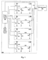
- Multiphase power supply 100 comprises a plurality of synchronous switching regulators designated as 110A, 110B, 110C and 110D. Synchronous switching regulators 110A-D may, individually or collectively be referred to as switching regulator 110 or switching regulators 110, respectively. Switching regulators 110 are coupled to provide power to a microprocessor 160 at node 170. Multiphase power supply 100 further comprises a phase control circuit 150 coupled to each of switching regulators 110. It is important to note that different embodiments may comprise more or less than four switching regulators.
- each switching regulator 110 includes a pair of transistors (e.g., transistors 101 and 102, transistors 111 and 112, etc.) coupled between a power supply terminal Vcc and ground.
- Each switching regulator 110 further includes a diode (e.g., diodes 103, 113, etc.), an inductor (e.g. inductors 104, 114, etc.) and a capacitor (e.g., capacitors 105, 115, etc.). It is noted that other specific circuit arrangements may be employed to implement each switching regulator 110.
- Phase control circuit 150 is configured to generate a plurality of control signals for controlling the states of the transistors in switching regulators 110 such that the switching regulators 110 operate out of phase with respect to one another.
- phase control circuit 150 may include a Semtech SC1144 integrated circuit.
- phase control circuit 150 also includes further circuitry to selectively suspend operation of a subset of switching regulators 110 during a low power mode of operation to thereby allow for improved efficiency.
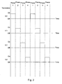
- Figures 2-4 illustrate aspects of the operation of multiphase power supply 100.
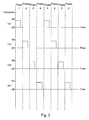
- Figures 2 and 3 are timing diagrams illustrating exemplary duty cycles associated with transistors 101, 111, 121 and 131 during a normal mode of operation.
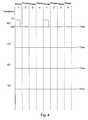
- Figure 4 is a timing diagram illustrating exemplary duty cycles associated with transistors 101, 111, 121 and 131 during a low power mode of operation.
- phase control circuit 150 activates (i.e. turns on) transistors 101,111,121 and 131, respectively, during different phases of operation.
- transistor 101 is turned on while transistors 111, 121 and 131 are turned off.
- each switching regulator 110 is embodied as a synchronous regulator, when transistor 101 is turned on, transistor 102 is turned off (in response to a corresponding control signal from phase control circuit 150).
- current flows from Vcc through transistor 101 and inductor 104 to charge capacitor 105.
- transistors 111, 121 and 131 are turned off, and transistors 112, 122 and 132 are turned on.
- phase control circuit 150 turns off transistor 101 and turns on transistor 102.
- transistor 102 When transistor 102 is turned on and transistor 101 is turned off, current may continue to temporarily flow through inductor 104 to charge capacitor 105 since current flow through inductor 104 cannot change instantaneously.
- Transistor 102 provides a return path for this current.
- phase 2 transistor 111 of switching regulator 110B is turned on and transistor 112 is turned off. Consequently, similar to the previous discussion, capacitor 115 is charged by current flow from Vcc through transistor 111. Subsequent operations of switching regulators 510C and 510D during phases 3 and 4 are similar.
- Phase control circuit 150 may be further configured to monitor the output voltage, Vout, at node 170 via a feedback control signal and adjust accordingly the duty cycle of transistors 101, 111, 121 and 131 to maintain a constant voltage level.
- Figure 3 illustrates an exemplary situation where the duty cycle of transistors 101, 111, 121 and 131 of Figure 1 is lessened due to, for example, reduced current draw by microprocessor 160.
- the duty cycle of transistors 101, 111, 121 and 131 would increase relative to the example of Figure 2 if there were a decreased output voltage at node 170, i.e., due to increased current draw by microprocessor 160.
- microprocessor 160 is configured to operate in a low power mode of operation. During such mode of operation, microprocessor 160 requires less current.
- the low power mode of operation may be controlled by, for example, a power management unit (not shown) which detects certain system inactivity, as desired.
- Phase control circuit 150 is configured to selectively suspend operation of a subset of switching regulators 110 (e.g. switching regulators 110B, 110C and 110D) upon assertion of a low power mode control signal which indicates that microprocessor 160 is currently operating in a low power mode.
- the low power mode control signal may be received from the power management unit.
- phase control circuit 150 suspends operation of switching regulator circuits 110B, 110C and 110D during the low power mode by removing (or otherwise driving or disabling) the control signals provided to the associated switching transistors 111, 112, 121, 122, 131 and 132 such that the transistors are held in an off state.
- switching regulator 110A operates in its normal manner as described previously.
- FIG. 5 illustrates another embodiment of a multiphase power supply 500.
- Multiphase power supply 500 of Figure 5 differs from multiphase power supply 100 of Figure 1 in that transistors 102, 112, 122 and 132 have been omitted.
- the switching regulators, e.g. 510A, 510B, 510C and 510D, of Figure 5 are not synchronous regulators.
- a respective diode i.e., diode 503, 513, 523 or 533, of each switching regulator 510 provides a return path for current to flow when the associated transistor, i.e., transistor 501, 511, 521 or 531, is turned off.
- Various embodiments of the multiphase power supply may advantageously allow for relatively high current capabilities during a normal mode of operation, while minimizing losses during the low power mode of operation.
- By suspending operation of a subset of switching regulators during the low power mode of operation capacitive switching losses associated with the transistors of the suspended switching regulators may be eliminated. Therefore, overall efficiency of the power supply may be improved.
- This invention is applicable to power supplies.
Landscapes
- Engineering & Computer Science (AREA)
- Power Engineering (AREA)
- Dc-Dc Converters (AREA)
Description
- The present invention relates to the field of power supplies, and more particularly to multiphase switching power supplies.
- Power supplies are used in various types of devices. There are many specialized types of power supply circuits with various advantages and disadvantages. Microprocessors in computers may require a power supply circuit that regulates a high level of current while maintaining a high level of efficiency.
- One such type of specialized power supply circuit is a switching regulator. Switching regulators typically provide an output with a lower voltage than the unregulated input while at the same time providing an output with a higher current than the current drawn from the unregulated supply. This is accomplished by a passive transistor that is constantly switching between the saturation mode and the nonconducting mode. Because the passive transistor is either in saturation or not conducting, there is very low power dissipation. A switching regulator therefore can regulate a high amount of current at a high efficiency rate.
- A disadvantage with switching regulators is known as the "ripple effect." The ripple effect refers to ripples that are periodic variations in the output voltage that have to be smoothed out in order to generate a genuine DC current. The ripple effect problem may be reduced or eliminated by coupling multiple switching regulators in parallel and operating them such that they are out of phase with respect to one another. This configuration is known as a multiphase switching regulator. A multiphase switching regulator typically produces a high current output with high efficiency while at the same time reducing ripple. Consequently, a multiphase switching regulator is a popular choice for use in a power supply circuit where high levels of current and efficiency are desired.
- Many microprocessors are configured to selectively operate in a low power mode of operation. During low power mode, the microprocessor may be configured to power down certain functional blocks (e.g. those that are inactive) and/or reduce the frequency of its internal clock(s). Powering down certain portions of the microprocessor and/or reducing clocking frequencies may advantageously reduce power consumption. When the microprocessor returns to a normal mode of operation, the microprocessor draws relatively higher amounts of current.
- Unfortunately, when the microprocessor is operating in low power mode, a multiphase switching regulator becomes more inefficient as a percentage of the total current generated. This is because the transistors in the switching regulators continue to switch at the same frequency as during the normal mode of operation. Since the transistors are switching at the same frequency, the capacitive losses associated with the switching are the same during the low power and normal modes of operation. However, since less current is drawn during the low power mode of operation, the switching becomes more inefficient as a percentage of the total current generated. Therefore, an improved multiphase power supply circuit is desired that will lower switching-related power losses during low power modes of operation.
- The article of G. Hua and F. Lee : "Soft switching PWM techniques and their applications", EPE Brighton '93, discloses a power supply according to the preamble of
claim 1. - The problems outlined above may in large part be solved by a power supply that lowers power losses during a low power mode of operation. In one embodiment, a multiphase power supply includes four switching regulators coupled in parallel with respect to one another. Each switching regulator may operate concurrently, and each may be controlled out of phase with respect to one another. In a particular embodiment, each switching regulator may be a synchronous switching regulator. The multiphase power supply further includes a phase control circuit coupled to the plurality of switching regulators. The phase control circuit is configured to selectively suspend operation of at least one of the switching regulators during a low power mode of operation. The phase control circuit may further be configured to control the switching of the switching regulators so that they are out of phase with respect to one another.
- Various embodiments of the multiphase power supply may advantageously allow for relatively high current capabilities during a normal mode of operation, while minimizing losses during the low power mode of operation. By suspending operation of a subset of switching regulators during the low power mode of operation, capacitive switching losses associated with the transistors of the suspended switching regulators may be eliminated. Therefore, overall efficiency of the power supply may be improved.
- The invention is set forth in
claim 1. - A better understanding of the present invention can be obtained when the following detailed description of the preferred embodiment is considered in conjunction with the following drawings, in which:
-
Figure 1 illustrates a particular embodiment of a multiphase power supply; -
Figure 2 is a timing diagram illustrating the duty cycles of selected transistors ofFigure 1 during a normal mode of operation; -
Figure 3 is a timing diagram illustrating reduced duty cycles of selected transistors ofFigure 1 during a normal mode of operation; -
Figure 4 is a timing diagram illustrating the duty cycles of selected transistors ofFigure 1 during a low power mode of operation; and -
Figure 5 illustrates another embodiment of a multiphase power supply. - While the invention is susceptible to various modifications and alternative forms, specific embodiments thereof are shown by way of example in the drawings and will herein be described in detail. It should be understood, however, that the drawings and detailed description thereto are not intended to limit the invention to the particular form disclosed, but on the contrary, the intention is to cover all modifications, equivalents and alternatives falling within the spirit and scope of the present invention as defined by the appended claims.
-
Figure 1 illustrates a particular embodiment of a multiphase power supply 100. Multiphase power supply 100 comprises a plurality of synchronous switching regulators designated as 110A, 110B, 110C and 110D.Synchronous switching regulators 110A-D may, individually or collectively be referred to as switching regulator 110 or switching regulators 110, respectively. Switching regulators 110 are coupled to provide power to amicroprocessor 160 atnode 170. Multiphase power supply 100 further comprises aphase control circuit 150 coupled to each of switching regulators 110. It is important to note that different embodiments may comprise more or less than four switching regulators. - In the illustrated embodiment each switching regulator 110 includes a pair of transistors (e.g.,
transistors transistors diodes e.g. inductors capacitors -
Phase control circuit 150 is configured to generate a plurality of control signals for controlling the states of the transistors in switching regulators 110 such that the switching regulators 110 operate out of phase with respect to one another. In a particular embodiment,phase control circuit 150 may include a Semtech SC1144 integrated circuit. As will be described in further detail below,phase control circuit 150 also includes further circuitry to selectively suspend operation of a subset of switching regulators 110 during a low power mode of operation to thereby allow for improved efficiency. -
Figures 2-4 illustrate aspects of the operation of multiphase power supply 100.Figures 2 and3 are timing diagrams illustrating exemplary duty cycles associated withtransistors Figure 4 is a timing diagram illustrating exemplary duty cycles associated withtransistors - Turning collectively to
Figures 1 and2 ,phase control circuit 150 activates (i.e. turns on) transistors 101,111,121 and 131, respectively, during different phases of operation. During a first phase of operation ("phase 1"),transistor 101 is turned on whiletransistors transistor 101 is turned on,transistor 102 is turned off (in response to a corresponding control signal from phase control circuit 150). Thus, duringphase 1. current flows from Vcc throughtransistor 101 andinductor 104 to chargecapacitor 105. Also duringphase 1,transistors transistors - During the next phase of operation ("
phase 2"),phase control circuit 150 turns offtransistor 101 and turns ontransistor 102. Whentransistor 102 is turned on andtransistor 101 is turned off, current may continue to temporarily flow throughinductor 104 to chargecapacitor 105 since current flow throughinductor 104 cannot change instantaneously.Transistor 102 provides a return path for this current. - Also during
phase 2,transistor 111 of switchingregulator 110B is turned on andtransistor 112 is turned off. Consequently, similar to the previous discussion,capacitor 115 is charged by current flow from Vcc throughtransistor 111. Subsequent operations of switchingregulators phases -
Phase control circuit 150 may be further configured to monitor the output voltage, Vout, atnode 170 via a feedback control signal and adjust accordingly the duty cycle oftransistors Figure 3 illustrates an exemplary situation where the duty cycle oftransistors Figure 1 is lessened due to, for example, reduced current draw bymicroprocessor 160. The duty cycle oftransistors Figure 2 if there were a decreased output voltage atnode 170, i.e., due to increased current draw bymicroprocessor 160. - As stated previously,
microprocessor 160 is configured to operate in a low power mode of operation. During such mode of operation,microprocessor 160 requires less current. The low power mode of operation may be controlled by, for example, a power management unit (not shown) which detects certain system inactivity, as desired.Phase control circuit 150 is configured to selectively suspend operation of a subset of switching regulators 110 (e.g. switching regulators microprocessor 160 is currently operating in a low power mode. The low power mode control signal may be received from the power management unit. As depicted inFigure 4 , in this embodiment,phase control circuit 150 suspends operation of switchingregulator circuits transistors regulator 110A operates in its normal manner as described previously. -
Figure 5 illustrates another embodiment of a multiphase power supply 500. Multiphase power supply 500 ofFigure 5 differs from multiphase power supply 100 ofFigure 1 in thattransistors Figure 5 are not synchronous regulators. A respective diode i.e.,diode transistor - Various embodiments of the multiphase power supply may advantageously allow for relatively high current capabilities during a normal mode of operation, while minimizing losses during the low power mode of operation. By suspending operation of a subset of switching regulators during the low power mode of operation, capacitive switching losses associated with the transistors of the suspended switching regulators may be eliminated. Therefore, overall efficiency of the power supply may be improved.
- While in the above described embodiments during the low power mode of operation all but one of the switching regulators is suspended from operation, other embodiments are possible where any number of switching regulators may be suspended.
- Numerous variations and modifications are possible within the scope of the appended claims.
- This invention is applicable to power supplies.
Claims (5)
- A power supply comprising:a first switching regulator circuit (110A);a second switching regulator circuit (110B);a third switching regulator circuit (110C);a fourth switching regulator circuit (110D);a phase control circuit (150) coupled to said first switching regulator circuit, said second switching regulator circuit, said third switching regulator circuit and said fourth switching regulator circuit, wherein said phase control circuit is configured to generate a plurality of switching control signals for controlling switching of said first, second, third and fourth switching regulator circuits;wherein each of the first, second, third and fourth switching regulator circuits includes an inductor (104, 114, 124, 134) coupled to a first transistor (101, 111, 121, 131) and a second transistor (102, 112, 122, 132), wherein the first transistor is coupled to pass current from a power source to said inductor when activated and wherein said second transistor is coupled to pass current from a ground node to said inductor when activated, and wherein said phase control circuit is configured to activate said first and second transistors out of phase with respect to each other; characterized in that said phase control circuit is configured to selectively suspend operation of said second, third and fourth switching regulator circuits in response to receiving a signal indicative of a low power mode of operation.
- A power supply as claimed in claim 1, wherein said phase control circuit (150) selectively suspends operation of said second switching regulator. (110B) circuit during said low power mode of operation by disabling at least one of said plurality of control signals to said second switching regulator circuit.
- A power supply as claimed in claim 1 or claim 2, wherein said phase control circuit (150) selectively activates and deactivates said first and second switching regulator circuits so that said first and second switching regulator circuits are out of phase with respect to one another.
- A power supply as claimed in any one of the preceding claims, wherein each of said first and second switching regulator circuits further comprises:a capacitor (105, 115) coupled to receive current flowing through said inductor. -
- A computer system comprising:a microprocessor;a power supply as claimed in any of claims 1-4 coupled to said microprocessor.
Applications Claiming Priority (3)
| Application Number | Priority Date | Filing Date | Title |
|---|---|---|---|
| US09/523,107 US6281666B1 (en) | 2000-03-14 | 2000-03-14 | Efficiency of a multiphase switching power supply during low power mode |
| US523107 | 2000-03-14 | ||
| PCT/US2000/031957 WO2001069768A1 (en) | 2000-03-14 | 2000-11-21 | Improved efficiency of a multiphase switching power supply during low power mode |
Publications (2)
| Publication Number | Publication Date |
|---|---|
| EP1264391A1 EP1264391A1 (en) | 2002-12-11 |
| EP1264391B1 true EP1264391B1 (en) | 2010-08-04 |
Family
ID=24083687
Family Applications (1)
| Application Number | Title | Priority Date | Filing Date |
|---|---|---|---|
| EP00980615A Expired - Lifetime EP1264391B1 (en) | 2000-03-14 | 2000-11-21 | Improved efficiency of a multiphase switching power supply during low power mode |
Country Status (7)
| Country | Link |
|---|---|
| US (1) | US6281666B1 (en) |
| EP (1) | EP1264391B1 (en) |
| JP (1) | JP2003527062A (en) |
| KR (1) | KR100698499B1 (en) |
| CN (1) | CN1264270C (en) |
| DE (1) | DE60044785D1 (en) |
| WO (1) | WO2001069768A1 (en) |
Cited By (1)
| Publication number | Priority date | Publication date | Assignee | Title |
|---|---|---|---|---|
| EP2582041A3 (en) * | 2011-10-14 | 2017-01-11 | Samsung Electronics Co., Ltd | Apparatus and Method for Interleaving Switching in Power Amplifier |
Families Citing this family (69)
| Publication number | Priority date | Publication date | Assignee | Title |
|---|---|---|---|---|
| DE60030424D1 (en) * | 1999-03-23 | 2006-10-12 | Advanced Energy Ind Inc | DC-POWERED COMPUTER SYSTEM WITH A HIGH-FREQUENCY SWITCHING POWER SUPPLY |
| US6694438B1 (en) | 1999-07-02 | 2004-02-17 | Advanced Energy Industries, Inc. | System for controlling the delivery of power to DC computer components |
| US6545450B1 (en) * | 1999-07-02 | 2003-04-08 | Advanced Energy Industries, Inc. | Multiple power converter system using combining transformers |
| US6278263B1 (en) * | 1999-09-01 | 2001-08-21 | Intersil Corporation | Multi-phase converter with balanced currents |
| US6803752B1 (en) * | 2000-02-14 | 2004-10-12 | Linear Technology Corporation | Polyphase PWM regulator with high efficiency at light loads |
| US6674274B2 (en) * | 2001-02-08 | 2004-01-06 | Linear Technology Corporation | Multiple phase switching regulators with stage shedding |
| GB2407882B (en) * | 2001-02-08 | 2005-11-02 | Linear Techn Inc | Multiple phase switching regulators with stage shedding |
| SE0102230L (en) * | 2001-06-25 | 2002-12-26 | Ragnar Joensson | Switching circuit with multiple steps |
| US20040233690A1 (en) * | 2001-08-17 | 2004-11-25 | Ledenev Anatoli V. | Multiple power converter system using combining transformers |
| US6970364B2 (en) * | 2002-03-08 | 2005-11-29 | University Of Central Florida | Low cost AC/DC converter with power factor correction |
| US7218085B2 (en) * | 2002-05-24 | 2007-05-15 | Arizona Board Of Regents | Integrated ZVS synchronous buck DC-DC converter with adaptive control |
| AU2003243515A1 (en) * | 2002-06-13 | 2003-12-31 | Pei Electronics, Inc. | Improved pulse forming converter |
| US7301408B2 (en) | 2002-10-15 | 2007-11-27 | Marvell World Trade Ltd. | Integrated circuit with low dielectric loss packaging material |
| US8952776B2 (en) * | 2002-12-13 | 2015-02-10 | Volterra Semiconductor Corporation | Powder core material coupled inductors and associated methods |
| US7109689B2 (en) * | 2003-04-04 | 2006-09-19 | Intersil Americas Inc. | Transient-phase PWM power supply and method |
| US7298197B2 (en) * | 2003-08-18 | 2007-11-20 | Nxp B.V. | Multi-phase DC-DC converter with shared control |
| US7265522B2 (en) * | 2003-09-04 | 2007-09-04 | Marvell World Trade Ltd. | Dynamic multiphase operation |
| TW589791B (en) * | 2003-09-04 | 2004-06-01 | Micro Star Int Co Ltd | Synchronous parallel voltage conversion device |
| JP3851303B2 (en) * | 2003-09-08 | 2006-11-29 | ローム株式会社 | Multi-output type power supply device and portable device using the same |
| JP4637855B2 (en) * | 2003-12-22 | 2011-02-23 | コーニンクレッカ フィリップス エレクトロニクス エヌ ヴィ | Switch mode power supply |
| DE112005000388T5 (en) * | 2004-02-17 | 2007-02-08 | Agere Systems, Inc. | Versatile and intelligent power controller |
| US7190210B2 (en) * | 2004-03-25 | 2007-03-13 | Integral Wave Technologies, Inc. | Switched-capacitor power supply system and method |
| US7239194B2 (en) * | 2004-03-25 | 2007-07-03 | Integral Wave Technologies, Inc. | Trench capacitor power supply system and method |
| US8324872B2 (en) * | 2004-03-26 | 2012-12-04 | Marvell World Trade, Ltd. | Voltage regulator with coupled inductors having high coefficient of coupling |
| US7234055B2 (en) * | 2004-08-24 | 2007-06-19 | Inventec Corporation | Computer operating booting system making use of multi-buttons |
| US7315463B2 (en) * | 2004-09-30 | 2008-01-01 | Intel Corporation | Apparatus and method for multi-phase transformers |
| US20080207237A1 (en) * | 2005-04-14 | 2008-08-28 | Koninklijke Philips Electronics N.V. | Communication in Phase Shifted Driven Power Converters |
| US20060255777A1 (en) * | 2005-05-10 | 2006-11-16 | Koertzen Henry W | Apparatus and method for improving voltage converter low load efficiency |
| US7504808B2 (en) | 2005-06-30 | 2009-03-17 | Intel Corporation | Multiphase transformer for a multiphase DC-DC converter |
| US20070097571A1 (en) * | 2005-07-07 | 2007-05-03 | Intel Corporation | Multiphase voltage regulation using paralleled inductive circuits having magnetically coupled inductors |
| US7602155B2 (en) * | 2005-07-27 | 2009-10-13 | Artesyn Technologies, Inc. | Power supply providing ultrafast modulation of output voltage |
| US7294976B1 (en) | 2005-09-23 | 2007-11-13 | Advanced Micro Devices, Inc. | Split power supply subsystem with isolated voltage supplies to satisfy a predetermined power limit |
| JP4459918B2 (en) * | 2006-03-16 | 2010-04-28 | 富士通テン株式会社 | Switching regulator |
| KR100849215B1 (en) * | 2007-01-17 | 2008-07-31 | 삼성전자주식회사 | Power control apparatus, method, and system thereof |
| US7859336B2 (en) * | 2007-03-13 | 2010-12-28 | Astec International Limited | Power supply providing ultrafast modulation of output voltage |
| US8618788B2 (en) * | 2007-03-30 | 2013-12-31 | Malay Trivedi | Dynamically adjusted multi-phase regulator |
| US7737669B2 (en) * | 2007-03-30 | 2010-06-15 | Intel Corporation | Hierarchical control for an integrated voltage regulator |
| JP5049637B2 (en) * | 2007-04-12 | 2012-10-17 | 三菱電機株式会社 | DC / DC power converter |
| US7812581B2 (en) * | 2007-05-04 | 2010-10-12 | Intersil Americas Inc. | Pulse adding scheme for smooth phase dropping at light load conditions for multiphase voltage regulators |
| CN101350557B (en) * | 2007-07-18 | 2011-04-27 | 华为技术有限公司 | Apparatus for adjusting power supply |
| US7994761B2 (en) * | 2007-10-08 | 2011-08-09 | Astec International Limited | Linear regulator with RF transistors and a bias adjustment circuit |
| US8183841B2 (en) * | 2008-01-07 | 2012-05-22 | Semiconductor Components Industries, Llc | Multi-phase power supply controller and method therefor |
| US7999520B2 (en) * | 2008-04-23 | 2011-08-16 | Dell Products L.P. | Static phase shedding for voltage regulators based upon circuit identifiers |
| JP5275688B2 (en) * | 2008-06-04 | 2013-08-28 | 住友重機械工業株式会社 | Converter device |
| US8228049B2 (en) * | 2008-07-14 | 2012-07-24 | Intersil Americas LLC | Advanced phase number control for multiphase converters |
| US7948222B2 (en) | 2009-02-05 | 2011-05-24 | Advanced Micro Devices, Inc. | Asymmetric topology to boost low load efficiency in multi-phase switch-mode power conversion |
| US8930723B2 (en) | 2009-10-07 | 2015-01-06 | Dell Products L.P. | System and method for multi-phase voltage regulation |
| JP5519404B2 (en) | 2010-05-25 | 2014-06-11 | 国立大学法人豊橋技術科学大学 | Switching circuit and envelope signal amplifier |
| CN102457167B (en) * | 2010-10-19 | 2016-03-16 | 雅达电子国际有限公司 | Many level parallel power converters |
| WO2013024172A1 (en) * | 2011-08-17 | 2013-02-21 | Belenos Clean Power Holding Ag | Dc/dc converter for hybrid system |
| JP5779043B2 (en) * | 2011-08-23 | 2015-09-16 | 株式会社東芝 | DC-DC converter and information processing apparatus |
| WO2013047543A1 (en) * | 2011-09-28 | 2013-04-04 | 三洋電機株式会社 | Power controller |
| JP5741365B2 (en) * | 2011-10-14 | 2015-07-01 | 富士通株式会社 | Regulator device |
| TWI462430B (en) * | 2012-02-02 | 2014-11-21 | Wistron Corp | Power management system |
| JP5998739B2 (en) * | 2012-08-20 | 2016-09-28 | 富士通株式会社 | Regulator device |
| US9287778B2 (en) | 2012-10-08 | 2016-03-15 | Nvidia Corporation | Current parking response to transient load demands |
| US9178421B2 (en) | 2012-10-30 | 2015-11-03 | Nvidia Corporation | Multi-stage power supply with fast transient response |
| US9000786B2 (en) | 2013-02-15 | 2015-04-07 | Dell Products Lp | Methods and systems for defective phase identification and current sense calibration for multi-phase voltage regulator circuits |
| JP2015128340A (en) * | 2013-12-27 | 2015-07-09 | 株式会社オートネットワーク技術研究所 | Step-down device and step-up device |
| KR20160096477A (en) * | 2015-02-05 | 2016-08-16 | 주식회사 현대아이티 | Multiple power board energy consumption reduction device of smartboard |
| US9899920B2 (en) * | 2015-09-11 | 2018-02-20 | Mediatek Inc. | Voltage regulator and method for controlling output stages of voltage regulator |
| AT517686B1 (en) * | 2015-10-01 | 2017-04-15 | Avl List Gmbh | Method for driving a multiphase synchronous converter |
| US9658666B1 (en) * | 2015-12-18 | 2017-05-23 | Intel Corporation | Dynamic capacitor modulated voltage regulator |
| JP6650506B2 (en) | 2016-02-24 | 2020-02-19 | 本田技研工業株式会社 | Power supply device, device and control method |
| JP6461838B2 (en) | 2016-02-24 | 2019-01-30 | 本田技研工業株式会社 | Power supply device, device and control method |
| WO2017145305A1 (en) | 2016-02-24 | 2017-08-31 | 本田技研工業株式会社 | Power supply device, apparatus, and control method |
| CN108333531B (en) * | 2018-01-26 | 2021-03-09 | 苏州浪潮智能科技有限公司 | Multiphase switching power supply efficiency debugging device, method and system |
| CN109586556B (en) * | 2018-12-10 | 2020-02-07 | 郑州云海信息技术有限公司 | Multiphase pulse width voltage reduction regulating circuit and regulating method thereof |
| CN113157045B (en) | 2020-01-22 | 2023-10-24 | 台湾积体电路制造股份有限公司 | Voltage regulator circuit and method |
Family Cites Families (13)
| Publication number | Priority date | Publication date | Assignee | Title |
|---|---|---|---|---|
| US4270165A (en) * | 1979-04-24 | 1981-05-26 | Qualidyne Systems, Inc. | Controller for d.c. current supplied by a plurality of parallel power supplies |
| JPS63245254A (en) * | 1987-03-30 | 1988-10-12 | Toshiba Corp | Switching regulator |
| JPH07264776A (en) * | 1994-03-18 | 1995-10-13 | Fujitsu Ltd | Parallel connection controller for plurality of converters |
| JPH10133754A (en) * | 1996-10-28 | 1998-05-22 | Fujitsu Ltd | Regulator circuit and semiconductor integrated circuit device |
| JPH10304655A (en) * | 1997-04-21 | 1998-11-13 | Sony Corp | Switching regulator |
| JPH1132477A (en) * | 1997-07-09 | 1999-02-02 | New Japan Radio Co Ltd | Synchronous rectification switching power supply and semiconductor integrated circuit therefor |
| JPH11289755A (en) * | 1998-03-31 | 1999-10-19 | Fuji Electric Co Ltd | Protective circuit for multiple chopper device |
| JP2000014129A (en) * | 1998-06-22 | 2000-01-14 | Matsushita Electric Ind Co Ltd | Power device |
| US6144194A (en) | 1998-07-13 | 2000-11-07 | Linear Technology Corp. | Polyphase synchronous switching voltage regulators |
| US6055167A (en) * | 1998-08-10 | 2000-04-25 | Custom Power Systems, Inc. | Pulse width modulated boost converter integrated with power factor correction circuit |
| JP2000075943A (en) * | 1998-08-26 | 2000-03-14 | Hitachi Ltd | Power unit |
| US6031747A (en) | 1999-08-02 | 2000-02-29 | Lockheed Martin Missiles & Space Company | Interleaved synchronous flyback converter with high efficiency over a wide operating load range |
| US6137274A (en) | 2000-02-02 | 2000-10-24 | National Semiconductor Corporation | Switching DC-to-DC converter and conversion method with current sharing between paralleled channels |
-
2000
- 2000-03-14 US US09/523,107 patent/US6281666B1/en not_active Expired - Lifetime
- 2000-11-21 CN CNB008193118A patent/CN1264270C/en not_active Expired - Fee Related
- 2000-11-21 JP JP2001567117A patent/JP2003527062A/en active Pending
- 2000-11-21 WO PCT/US2000/031957 patent/WO2001069768A1/en active Application Filing
- 2000-11-21 EP EP00980615A patent/EP1264391B1/en not_active Expired - Lifetime
- 2000-11-21 KR KR1020027012083A patent/KR100698499B1/en not_active IP Right Cessation
- 2000-11-21 DE DE60044785T patent/DE60044785D1/en not_active Expired - Lifetime
Cited By (1)
| Publication number | Priority date | Publication date | Assignee | Title |
|---|---|---|---|---|
| EP2582041A3 (en) * | 2011-10-14 | 2017-01-11 | Samsung Electronics Co., Ltd | Apparatus and Method for Interleaving Switching in Power Amplifier |
Also Published As
| Publication number | Publication date |
|---|---|
| KR100698499B1 (en) | 2007-03-22 |
| KR20030069046A (en) | 2003-08-25 |
| WO2001069768A1 (en) | 2001-09-20 |
| US6281666B1 (en) | 2001-08-28 |
| CN1264270C (en) | 2006-07-12 |
| DE60044785D1 (en) | 2010-09-16 |
| EP1264391A1 (en) | 2002-12-11 |
| JP2003527062A (en) | 2003-09-09 |
| CN1451201A (en) | 2003-10-22 |
Similar Documents
| Publication | Publication Date | Title |
|---|---|---|
| EP1264391B1 (en) | Improved efficiency of a multiphase switching power supply during low power mode | |
| JP4025396B2 (en) | Switching voltage regulator circuit and method for controlling a switching voltage regulator | |
| US7071660B2 (en) | Two-stage voltage regulators with adjustable intermediate bus voltage, adjustable switching frequency, and adjustable number of active phases | |
| CN109586576B (en) | Feedback method for commanding a single-phase resonant converter, related single-phase resonant converter and multi-phase resonant converter | |
| JP5942455B2 (en) | Switching regulator | |
| US7872454B2 (en) | Digital low dropout regulator | |
| US6696825B2 (en) | DC-to-DC converter with fast override feedback control and associated methods | |
| US8214677B2 (en) | Voltage regulator with suspend mode | |
| US6249111B1 (en) | Dual drive buck regulator | |
| USRE38371E1 (en) | DC-to-DC controller having a multi-phase synchronous buck regulator | |
| US6362607B1 (en) | Gated multi-phase fixed duty cycle voltage regulator | |
| CN107947576B (en) | Low buck switching power supply with reduced switching losses | |
| CN112166547A (en) | Power management system | |
| KR20010014757A (en) | Multiple output buck converter with single inductor | |
| JP2008263771A (en) | Dynamically adjusted multi-phase regulator | |
| US6707280B1 (en) | Bidirectional voltage regulator sourcing and sinking current for line termination | |
| US11770073B2 (en) | Methods and apparatus for regulated hybrid converters | |
| US7046528B2 (en) | Load-dependent variable frequency voltage regulator | |
| US8286008B2 (en) | Multi-phase voltage regulator on motherboard | |
| US6721893B1 (en) | System for suspending operation of a switching regulator circuit in a power supply if the temperature of the switching regulator is too high | |
| US20010024113A1 (en) | Regulated auxiliary power supply | |
| JP6619662B2 (en) | Switching regulator | |
| CN104317379A (en) | System and method for supplying power for processor for providing dynamic working voltage | |
| US20070139020A1 (en) | Coupled inductor output regulation |
Legal Events
| Date | Code | Title | Description |
|---|---|---|---|
| PUAI | Public reference made under article 153(3) epc to a published international application that has entered the european phase |
Free format text: ORIGINAL CODE: 0009012 |
|
| 17P | Request for examination filed |
Effective date: 20020927 |
|
| AK | Designated contracting states |
Kind code of ref document: A1 Designated state(s): AT BE CH CY DE DK ES FI FR GB GR IE IT LI LU MC NL PT SE TR |
|
| RIN1 | Information on inventor provided before grant (corrected) |
Inventor name: HERNANDEZ, CARL Inventor name: TRESSLER, CHRIS Inventor name: CHEN, MARY |
|
| RBV | Designated contracting states (corrected) |
Designated state(s): AT BE DE GB |
|
| RAP1 | Party data changed (applicant data changed or rights of an application transferred) |
Owner name: GLOBALFOUNDRIES, INC. |
|
| GRAP | Despatch of communication of intention to grant a patent |
Free format text: ORIGINAL CODE: EPIDOSNIGR1 |
|
| GRAS | Grant fee paid |
Free format text: ORIGINAL CODE: EPIDOSNIGR3 |
|
| GRAA | (expected) grant |
Free format text: ORIGINAL CODE: 0009210 |
|
| AK | Designated contracting states |
Kind code of ref document: B1 Designated state(s): DE GB |
|
| REG | Reference to a national code |
Ref country code: GB Ref legal event code: FG4D |
|
| REF | Corresponds to: |
Ref document number: 60044785 Country of ref document: DE Date of ref document: 20100916 Kind code of ref document: P |
|
| PLBE | No opposition filed within time limit |
Free format text: ORIGINAL CODE: 0009261 |
|
| STAA | Information on the status of an ep patent application or granted ep patent |
Free format text: STATUS: NO OPPOSITION FILED WITHIN TIME LIMIT |
|
| 26N | No opposition filed |
Effective date: 20110506 |
|
| PGFP | Annual fee paid to national office [announced via postgrant information from national office to epo] |
Ref country code: GB Payment date: 20110221 Year of fee payment: 11 Ref country code: DE Payment date: 20110228 Year of fee payment: 11 |
|
| REG | Reference to a national code |
Ref country code: DE Ref legal event code: R097 Ref document number: 60044785 Country of ref document: DE Effective date: 20110506 |
|
| GBPC | Gb: european patent ceased through non-payment of renewal fee |
Effective date: 20111121 |
|
| PG25 | Lapsed in a contracting state [announced via postgrant information from national office to epo] |
Ref country code: GB Free format text: LAPSE BECAUSE OF NON-PAYMENT OF DUE FEES Effective date: 20111121 |
|
| REG | Reference to a national code |
Ref country code: DE Ref legal event code: R119 Ref document number: 60044785 Country of ref document: DE Effective date: 20130601 |
|
| PG25 | Lapsed in a contracting state [announced via postgrant information from national office to epo] |
Ref country code: DE Free format text: LAPSE BECAUSE OF NON-PAYMENT OF DUE FEES Effective date: 20130601 |