EP1263208B1 - Method for generating unique image sensor indentification, and image sensor system for use therewith - Google Patents
Method for generating unique image sensor indentification, and image sensor system for use therewith Download PDFInfo
- Publication number
- EP1263208B1 EP1263208B1 EP01304718.8A EP01304718A EP1263208B1 EP 1263208 B1 EP1263208 B1 EP 1263208B1 EP 01304718 A EP01304718 A EP 01304718A EP 1263208 B1 EP1263208 B1 EP 1263208B1
- Authority
- EP
- European Patent Office
- Prior art keywords
- image sensor
- digital
- image
- key
- fpn
- Prior art date
- Legal status (The legal status is an assumption and is not a legal conclusion. Google has not performed a legal analysis and makes no representation as to the accuracy of the status listed.)
- Expired - Lifetime
Links
Images


Classifications
-
- H—ELECTRICITY
- H04—ELECTRIC COMMUNICATION TECHNIQUE
- H04N—PICTORIAL COMMUNICATION, e.g. TELEVISION
- H04N1/00—Scanning, transmission or reproduction of documents or the like, e.g. facsimile transmission; Details thereof
- H04N1/32—Circuits or arrangements for control or supervision between transmitter and receiver or between image input and image output device, e.g. between a still-image camera and its memory or between a still-image camera and a printer device
- H04N1/32101—Display, printing, storage or transmission of additional information, e.g. ID code, date and time or title
- H04N1/32128—Display, printing, storage or transmission of additional information, e.g. ID code, date and time or title attached to the image data, e.g. file header, transmitted message header, information on the same page or in the same computer file as the image
-
- H—ELECTRICITY
- H04—ELECTRIC COMMUNICATION TECHNIQUE
- H04N—PICTORIAL COMMUNICATION, e.g. TELEVISION
- H04N2201/00—Indexing scheme relating to scanning, transmission or reproduction of documents or the like, and to details thereof
- H04N2201/32—Circuits or arrangements for control or supervision between transmitter and receiver or between image input and image output device, e.g. between a still-image camera and its memory or between a still-image camera and a printer device
- H04N2201/3201—Display, printing, storage or transmission of additional information, e.g. ID code, date and time or title
- H04N2201/3204—Display, printing, storage or transmission of additional information, e.g. ID code, date and time or title of data relating to a user, sender, addressee, machine or electronic recording medium
- H04N2201/3205—Display, printing, storage or transmission of additional information, e.g. ID code, date and time or title of data relating to a user, sender, addressee, machine or electronic recording medium of identification information, e.g. name or ID code
-
- H—ELECTRICITY
- H04—ELECTRIC COMMUNICATION TECHNIQUE
- H04N—PICTORIAL COMMUNICATION, e.g. TELEVISION
- H04N2201/00—Indexing scheme relating to scanning, transmission or reproduction of documents or the like, and to details thereof
- H04N2201/32—Circuits or arrangements for control or supervision between transmitter and receiver or between image input and image output device, e.g. between a still-image camera and its memory or between a still-image camera and a printer device
- H04N2201/3201—Display, printing, storage or transmission of additional information, e.g. ID code, date and time or title
- H04N2201/3212—Display, printing, storage or transmission of additional information, e.g. ID code, date and time or title of data relating to a job, e.g. communication, capture or filing of an image
- H04N2201/3215—Display, printing, storage or transmission of additional information, e.g. ID code, date and time or title of data relating to a job, e.g. communication, capture or filing of an image of a time or duration
Definitions
- This invention relates to a method for generating a unique identification which can be used to establish that a given image or series of images has originated from a particular image sensor, and to an image sensor system for operating the method.
- the present invention is based on generating and using a unique encryption key in a simple and cost effective manner.
- EP506469 discloses an apparatus for recognizing specific original patterns by examining a state of a function in order to prevent fraudulous copy of the specific original.
- the invention provides a method of generating a unique identification for an image sensor of a type which produces fixed pattern noise, the method comprising disabling a fixed pattern noise cancellation to measure the fixed pattern noise when taking reference image data, using a measurement of the fixed pattern noise to generate a numeric key, enabling the fixed pattern noise cancellation and attaching to one or more images output by the image sensor a digital signature which is generated by combining the key and image data according to a predetermined algorithm.
- the invention provides an image sensor system comprising:
- a CMOS based integrated circuit image sensor has an array of pixels, only four of which are shown. Each pixel has a photosensitive element such as photodiode 10 and associated sense transistor M1 and reset transistor M2. As is well known, it is equally possible to have a single transistor, M1, per pixel, or to have additional transistors such as a photogate transistor.
- the sense transistor M1 has an inherent voltage drop Vt, known as the "threshold voltage", between its source and gate. Vt varies from one transistor to another due to manufacturing tolerances of factors such as oxide thickness and doping concentration. The signal available for a given pixel at the output is the photo-generated current minus Vt. Vt can vary as between transistors by as much as +/- 100mV in a voltage swing of 0.5 - 1.0 V.
- FPN Fixed Pattern Noise
- Image sensors may have one or more FPN circuits and one or more A-D converters (e.g. one per-chip, one per-column).
- the invention is based on the realisation that the FPN for any image sensor is unique to that sensor.
- the invention operates by temporarily disabling the FPN correction, and reading out the FPN as a unique set of characteristics to be used in generating a key for use in creating digital signatures.
- This procedure is typically performed during camera turn-on. It is not necessary to perform this more often, which would reduce the throughput of the camera, especially in video (motion) systems.
- the procedure may be carried out at each turn-on, and the result stored in a memory, or it may be performed only at the first power-on and the result stored permanently in a permanent memory such as a flash/OTP ROM.
- the FPN and hence the key, is produced as a result of the manufacturing process and is a feature of the most delicate part of the pixel. Once a sensor has been produced, it is practically impossible to alter it, at least without overt damage to the pixel.
- Various ways of producing the key from the FPN data are discussed below.
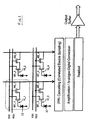
- Figure 3A illustrates the operation of the system once the key has been generated.
- the FPN cancellation is enabled once more, so that the image signals undergo FPN cancellation, amplification, and A-D conversion to produce a conventional digital signal at readout output 20.
- This signal is then further processed to produce a digital signature at 22, before being transmitted from the system via output buffer 24.
- digital signature generation is not significant in carrying out the invention.
- the methods used in the above-cited US Patents could be used.
- the presently preferred approach is to retrieve the key from store 26 and encrypt the key by means of a one-way algorithm at 28.
- the encrypted key is then applied to the image data as it is read out at 24 to generate the digital signature.
- This may be tagged to the end of the picture information as a discrete digital signature, or it may be embedded within the picture information (watermarking).
- each image has attached to it a unique digital signature which can be used to verify that image sensor as the source of the image by decoding through the appropriate algorithm and comparing with an encrypted key from that sensor.
- the digital signature can also verify that the image has not been altered, by checking the consistency of the image data with the signature.
- Fig. 3A deals with this by including time information in the digital signal generation.
- the time information is suitably derived from an external source by a receiver 30, which may be a MSF receiver for MSF time-reference radio broadcasts.
- a GPS receiver may be used to extract the time information encoded in GPS satellite signals.
- the time information could be generated off-chip, but this would provide opportunities to falsify the signal. It is therefore preferred for the time information to be generated on-chip with the whole system on a single chip.
- the time information may be derived from a free running clock circuit on-chip, which is synchronised periodically by the MSF or GPS signal.
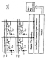
- the sequence of a series of images can be verified by generating a sequence of numbers and including these numbers in the in the digital signature generation in place of the time information as described above.
- Fig. 3B in which the receiver 30 of Fig. 3A is replaced by an image number sequence generator 31.
- the sequence generated could, for example, be reset at each power-on and could be a simple arithmetic series (e.g. 0,1,2... etc.) or the output from a pseudorandom number generator.
- the reference image may be a "black" image, which may be obtained by closing a shutter, if the image sensor forms part of a camera provided with a shutter.
- a shutter may not be practical, in which case a "black” image may be provided by reducing to a minimum the time during which the array is light sensitive. This can readily be as little as s which will be sufficiently small to render the array insensitive.
- the reference image may be an image obtained using some other predetermined illumination conditions (including zero or substantially zero illumination).
- Vt_a may vary between 550mV and 580mV, but if Vt_a»Vt_b this relationship will remain even if the temperature of the device varies.
- This factor is used in a first method, referring to Figure 5 . Pairs of pixels are compared. The number of pairs compared depends on the number of bits required for the key. The comparison used in this first method is: If Vt_a - Vt_b > threshold (region A), then output is 0 If Vt_b - Vt_a > threshold (region B), then output is 1 If Vt_a - Vt_b ⁇ threshold (region C) or Vt_b - Vt_a ⁇ threshold (region D), then the two threshold voltages are too close and this pair of pixels is ignored.
- a typical level of the threshold value would be 50mV.
- the foregoing method uses a fixed, predetermined threshold, which does not take into account the conditions of the camera device.
- An alternative, illustrated in Fig. 6 is to use an iterative process in which the threshold is increased. As this is done, an increasing number of pairs is classified as undecided, and the process is repeated until a desired number of pairs remains.
- the entire system is implemented as a single chip both for economy of manufacture and enhanced security. It is possible, however, for one or more elements of the system to be provided as separate circuits.
- the invention thus provides an improved and simplified means of verifying the source of images.
Description
- This invention relates to a method for generating a unique identification which can be used to establish that a given image or series of images has originated from a particular image sensor, and to an image sensor system for operating the method.
- There are many situations in which it is desirable to prove that a still or video image has been produced by a particular image sensor. Moreover, with the widespread availability of digital imaging technology, it can be necessary to prove that the image in question is original and has not been digitally manipulated after being captured.
- There are a number of prior art proposals for improving the security and authenticity of images, some of which are based on the use of encryption keys, for example
US 5,499,294 ,US 5,799,082 andUS 5,828,751 . InUS 5,499,294 , for example, a key is provided by calculating a unique key for each sensor and storing this key in the sensor during manufacture in a specially provided ROM store. Such methods thus require additional circuitry which must be programmable, and require a programming step to be carried out during manufacture, both of which increase costs. - The present invention is based on generating and using a unique encryption key in a simple and cost effective manner.
- Other prior art proposal such as
EP506469 - The invention provides a method of generating a unique identification for an image sensor of a type which produces fixed pattern noise, the method comprising disabling a fixed pattern noise cancellation to measure the fixed pattern noise when taking reference image data, using a measurement of the fixed pattern noise to generate a numeric key, enabling the fixed pattern noise cancellation and attaching to one or more images output by the image sensor a digital signature which is generated by combining the key and image data according to a predetermined algorithm.
- From another aspect, the invention provides an image sensor system comprising:
- an image sensor having an array of pixels forming an image plane, the pixels having a light sensitivity which varies from one pixel to another in a non-predictable manner to produce fixed pattern noise (FPN) unique to that image sensor;
- at least one FPN cancellation circuit connected to receive the output of the image sensor
- at least one analog to digital converter receiving the output of the FPN cancellation circuit to produce a digital image signal; and
- a digital signature generator which acts upon the digital image signal to incorporate therein a digital signature generated in accordance with a digital key;
- and in which said digital key is a function of the fixed pattern noise.
- Other features of the present invention are defined in the claims.
- Embodiments of the invention will now be described, by way of example, with reference to the drawings, in which:
-
Figure 1 is a schematic representation of a prior art image sensor; -
Figure 2 is a similar representation illustrating the principle of the present invention; -
Figure 3A illustrates in more detail one embodiment of the invention; -
Figure 3B illustrates a variation of the embodiment ofFig. 3B ; -
Figure 4 shows a modification ofFigure 3A ; -
Figure 5 illustrates one method of deriving a key from sensor pixel signals; and -
Figure 6 illustrates a modification of the method ofFigure 5 . - Referring to
Figure 1 , a CMOS based integrated circuit image sensor has an array of pixels, only four of which are shown. Each pixel has a photosensitive element such asphotodiode 10 and associated sense transistor M1 and reset transistor M2. As is well known, it is equally possible to have a single transistor, M1, per pixel, or to have additional transistors such as a photogate transistor. - The sense transistor M1 has an inherent voltage drop Vt, known as the "threshold voltage", between its source and gate. Vt varies from one transistor to another due to manufacturing tolerances of factors such as oxide thickness and doping concentration. The signal available for a given pixel at the output is the photo-generated current minus Vt. Vt can vary as between transistors by as much as +/- 100mV in a voltage swing of 0.5 - 1.0 V.
- Thus, variations in Vt across the array can cause large variations in image brightness, known as "Fixed Pattern Noise" (FPN). This is unacceptable, and it is usual to employ a mechanism to eliminate FPN.
- This is often combined with another noise cancelling technique: correlated double sampling. Using this technique, the reset value of the pixel is measured and stored. The signal value of the pixel is measured and subtracted. The subtraction cancels out the Vt:
- (1) Reset_Signal = Vreset + Vreset_noise - Vt
- (2) Pixel_Signal = Vreset + Vreset_noise - Vt - PhotoSignal
- (3) Reset_Signal - Pixel_Signal = PhotoSignal
- These signals are then usually amplified and converted to digital form before being read out.
- It will be understood that FPN cancellation and analog-digital conversion may be carried out in a number of ways. Image sensors may have one or more FPN circuits and one or more A-D converters (e.g. one per-chip, one per-column).
- The invention is based on the realisation that the FPN for any image sensor is unique to that sensor. Referring to
Figure 2 , the invention operates by temporarily disabling the FPN correction, and reading out the FPN as a unique set of characteristics to be used in generating a key for use in creating digital signatures. This procedure is typically performed during camera turn-on. It is not necessary to perform this more often, which would reduce the throughput of the camera, especially in video (motion) systems. The procedure may be carried out at each turn-on, and the result stored in a memory, or it may be performed only at the first power-on and the result stored permanently in a permanent memory such as a flash/OTP ROM. - The FPN, and hence the key, is produced as a result of the manufacturing process and is a feature of the most delicate part of the pixel. Once a sensor has been produced, it is practically impossible to alter it, at least without overt damage to the pixel.
- A practical image sensor has a large number of pixels, typically ranging from 100,000 for WebCam or low-quality TV to 3,000,000 for a high-end digital still camera. Thus the chances of two sensors having the same FPN is remote. If six pixel elements are used to produce a single key bit, even a low-end sensor with 100,000 pixels can generate a key of 216,666 = 105000 which is an enormous number, and hence the chance of any two sensors having the same key is extremely remote. Various ways of producing the key from the FPN data are discussed below.
-
Figure 3A illustrates the operation of the system once the key has been generated. The FPN cancellation is enabled once more, so that the image signals undergo FPN cancellation, amplification, and A-D conversion to produce a conventional digital signal atreadout output 20. This signal is then further processed to produce a digital signature at 22, before being transmitted from the system viaoutput buffer 24. - The particular form of digital signature generation used is not significant in carrying out the invention. For example, the methods used in the above-cited US Patents could be used. As seen in
Fig. 3A , the presently preferred approach is to retrieve the key fromstore 26 and encrypt the key by means of a one-way algorithm at 28. The encrypted key is then applied to the image data as it is read out at 24 to generate the digital signature. This may be tagged to the end of the picture information as a discrete digital signature, or it may be embedded within the picture information (watermarking). - In either case, each image has attached to it a unique digital signature which can be used to verify that image sensor as the source of the image by decoding through the appropriate algorithm and comparing with an encrypted key from that sensor. The digital signature can also verify that the image has not been altered, by checking the consistency of the image data with the signature.
- It is also frequently desired to be able to prove the time of an occurrence, or to prove that a series of images (which might be successive still images or a portion of motion video) occurred in a given sequence which has not been altered. The embodiment of
Fig. 3A deals with this by including time information in the digital signal generation. The time information is suitably derived from an external source by areceiver 30, which may be a MSF receiver for MSF time-reference radio broadcasts. Alternatively, a GPS receiver may be used to extract the time information encoded in GPS satellite signals. - The time information could be generated off-chip, but this would provide opportunities to falsify the signal. It is therefore preferred for the time information to be generated on-chip with the whole system on a single chip. In this case, the time information may be derived from a free running clock circuit on-chip, which is synchronised periodically by the MSF or GPS signal.
- As a simpler alternative in some circumstances, the sequence of a series of images can be verified by generating a sequence of numbers and including these numbers in the in the digital signature generation in place of the time information as described above. This is illustrated in
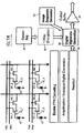
Fig. 3B , in which thereceiver 30 ofFig. 3A is replaced by an imagenumber sequence generator 31. The sequence generated could, for example, be reset at each power-on and could be a simple arithmetic series (e.g. 0,1,2... etc.) or the output from a pseudorandom number generator. - The system as thus far described will cause an image to be identified as invalid if it undergoes any processing after leaving the output buffer. It is common practice when dealing with colour systems to use post-processing of the signal after it leaves the image sensor chip. Therefore, as seen in
Figure 4 , where colour processing is desirable this must be included at 32 between readout and digital signal generation. Although the present invention is not limited to the entire system being on a single chip, this is the most secure way of implementing the invention. This is practical with modern, high-density CMOS technology; see for example S G Smith et al, "A Single-Chip CMOS 306x244 Pixel NTSC Video Camera and a Descendant Coprocessor Device", IEEE Journal Solid State Circuits, Vol 33, No 12, pp 2104-2111, December 1998. - Turning now to methods of generating the key from the variations in Vt, there are many robust methods of achieving this, some of which will be described.
- All require the measurement of the FPN. This is achieved by disabling the FPN correction system and taking a reference image. The reference image may be a "black" image, which may be obtained by closing a shutter, if the image sensor forms part of a camera provided with a shutter. However, a shutter may not be practical, in which case a "black" image may be provided by reducing to a minimum the time during which the array is light sensitive. This can readily be as little as s which will be sufficiently small to render the array insensitive. Alternatively, the reference image may be an image obtained using some other predetermined illumination conditions (including zero or substantially zero illumination).
- It is important to note that the absolute level of Vt will vary with environmental conditions such as temperature and current through the sense transistor. However, the relative values will not change: Vt_a may vary between 550mV and 580mV, but if Vt_a»Vt_b this relationship will remain even if the temperature of the device varies.
- This factor is used in a first method, referring to
Figure 5 . Pairs of pixels are compared. The number of pairs compared depends on the number of bits required for the key. The comparison used in this first method is:
If Vt_a - Vt_b > threshold (region A),
then output is 0
If Vt_b - Vt_a > threshold (region B),
then output is 1
If Vt_a - Vt_b < threshold (region C) or
Vt_b - Vt_a < threshold (region D),
then the two threshold voltages are too
close and this pair of pixels is ignored. - A typical level of the threshold value would be 50mV.
- An improvement on this technique is to read out a number of images and average them: this reduces the amount of noise.
- The foregoing method uses a fixed, predetermined threshold, which does not take into account the conditions of the camera device. An alternative, illustrated in
Fig. 6 , is to use an iterative process in which the threshold is increased. As this is done, an increasing number of pairs is classified as undecided, and the process is repeated until a desired number of pairs remains. - For example, in
Figure 6 it is desired to have a key generated from two pairs. Three pairs of pixels are compared and result in the values 1 (clearly in region A) and 2 (clearly in region B). Pair 3, however falls close to the original threshold (dotted line). It would be classified with the original threshold as region B, but as the threshold is increased 3 is dropped out as undecided. - This example allows six pixels to produce two, unambiguous bits of data. Obviously, a practical example would use a much larger set of pixels, but the principle would be the same.
- In both the foregoing methods, if a comparison is close to the threshold then a very small change will change the sensor key bit. A more robust method can be achieved by a fuzzy logic approach. With this technique a single dividing line is replaced by using a number of pairs of pixels to produce a single, but more reliable, sensor key bit. See H D Cheng et al., "Fuzzy homogeneity approach to multilevel thresholding", IEEE Trans. Image Processing, Vol 7, no 7, pp 1084-1088, July 1998. More generally, each of the binary digits of the key can be generated by measuring and processing a plurality of pixel signals.
- It is preferred that the entire system is implemented as a single chip both for economy of manufacture and enhanced security. It is possible, however, for one or more elements of the system to be provided as separate circuits.
- The invention thus provides an improved and simplified means of verifying the source of images.
Claims (16)
- A method of generating a unique digital identification associated with an image sensor of a type which produces fixed pattern noise, characterised in that the method comprises the steps of:- disabling a fixed pattern noise cancellation to measure the fixed pattern noise when taking reference image data,- using a measurement of the fixed pattern noise to generate a digital key,- enabling the fixed pattern noise cancellation,- combining the digital key and image data according to a predetermined algorithm to generate the unique digital identification, and- attaching to one or more images output by the image sensor the unique digital identification.
- The method of claim 1, further comprising generating the digital key from the values of pixel signals produced by the image sensor under predetermined illumination conditions.
- The method of claim 1 or claim 2, further comprising generating each binary digit of a plurality of binary digits of the key by measuring and processing a plurality of pixel signals.
- The method of claim 3, further comprising generating each binary digit of the plurality of binary digits by
comparing a given pair of pixel signals. - The method of claim 4, in which any given pair of pixel signals is ignored if their values do not differ by more than a predetermined threshold.
- The method of any preceding claim, in which each image has associated therewith a record of the time at which it was taken.
- The method of claim 6, in which said time record is included in the digital signature.
- An image sensor system comprising:an image sensor having an array of pixels forming an image plane, the pixels having a light sensitivity which varies from one pixel to another in a non-predictable manner to produce fixed pattern noise (FPN) unique to that image sensor;at least one FPN cancellation circuit connected to receive the output of the image sensor;at least one analog to digital converter receiving the output of the FPN cancellation circuit to produce a digital image signal; anda digital identification generator which acts upon the digital image signal to incorporate therein a digital identification generated in accordance with a digital key;and in which said digital key is a function of the fixed pattern noise.
- An image sensor system according to claim 8, including means for generating said digital key comprising means for disabling the at least one FPN cancellation circuit whereby the at least one analog to digital converter produces a digital image signal which includes FPN; a key generation circuit operable to generate a digital key by applying a predetermined calculation to the FPN; and a memory in which said digital key is stored.
- An image sensor system according to claim 9, in which said key generation circuit is arranged to measure and process the signal values of pluralities of pixels and to generate a binary digit from each plurality of pixel signals.
- An image sensor system according to any of claims 8 to 10, further including a timing circuit connected to the digital identification generator such that the digital signal for each image contains information defining the time when that image was taken.
- An image sensor system according to claim 11, in which the timing circuit is, or is synchronised by, a receiver for broadcast time signals.
- An image sensor system according to any of claims 8 to 10, further including a number sequence generator connected to the digital identification generator such that the digital identification for each image contains at least one number from said sequence.
- An image sensor system according to any of claims 8 to 13, in which the whole system is provided on a single chip.
- An image sensor system according to claim 14, further including a colour processing circuit interposed between the analog to digital converter and the digital signal generator.
- An image sensor system according to any of claim 8 to 15, in which the image sensor is a CMOS device in which each pixel comprises a light-sensitive circuit element and at least a sense transistor for sensing the charge on the light-sensitive circuit element; and in which the FPN is essentially a function of the threshold voltages of the sense transistors.
Priority Applications (2)
| Application Number | Priority Date | Filing Date | Title |
|---|---|---|---|
| EP01304718.8A EP1263208B1 (en) | 2001-05-29 | 2001-05-29 | Method for generating unique image sensor indentification, and image sensor system for use therewith |
| US10/156,721 US7129973B2 (en) | 2001-05-29 | 2002-05-28 | Method for generating unique image sensor identification, and image sensor system for use therewith |
Applications Claiming Priority (1)
| Application Number | Priority Date | Filing Date | Title |
|---|---|---|---|
| EP01304718.8A EP1263208B1 (en) | 2001-05-29 | 2001-05-29 | Method for generating unique image sensor indentification, and image sensor system for use therewith |
Publications (2)
| Publication Number | Publication Date |
|---|---|
| EP1263208A1 EP1263208A1 (en) | 2002-12-04 |
| EP1263208B1 true EP1263208B1 (en) | 2014-09-03 |
Family
ID=8181997
Family Applications (1)
| Application Number | Title | Priority Date | Filing Date |
|---|---|---|---|
| EP01304718.8A Expired - Lifetime EP1263208B1 (en) | 2001-05-29 | 2001-05-29 | Method for generating unique image sensor indentification, and image sensor system for use therewith |
Country Status (2)
| Country | Link |
|---|---|
| US (1) | US7129973B2 (en) |
| EP (1) | EP1263208B1 (en) |
Families Citing this family (32)
| Publication number | Priority date | Publication date | Assignee | Title |
|---|---|---|---|---|
| EP1263208B1 (en) * | 2001-05-29 | 2014-09-03 | STMicroelectronics Limited | Method for generating unique image sensor indentification, and image sensor system for use therewith |
| EP1408449A3 (en) * | 2002-10-04 | 2006-02-01 | Sony Corporation | Method and apparatus for identifying a photographic camera by correlating two images |
| JP3913224B2 (en) * | 2004-02-05 | 2007-05-09 | 株式会社リコー | Image processing apparatus and image forming apparatus |
| JP4556103B2 (en) * | 2004-02-24 | 2010-10-06 | ソニー株式会社 | Encryption apparatus and encryption method |
| US7609846B2 (en) * | 2004-07-13 | 2009-10-27 | Eastman Kodak Company | Matching of digital images to acquisition devices |
| JP4425834B2 (en) * | 2005-07-25 | 2010-03-03 | 富士フイルム株式会社 | Defective pixel update system |
| US7616237B2 (en) * | 2005-12-16 | 2009-11-10 | The Research Foundation Of State University Of New York | Method and apparatus for identifying an imaging device |
| US20080263361A1 (en) * | 2007-04-20 | 2008-10-23 | Microsoft Corporation | Cryptographically strong key derivation using password, audio-visual and mental means |
| US8027468B2 (en) * | 2008-04-08 | 2011-09-27 | Honeywell International Inc. | Method and system for camera sensor fingerprinting |
| EP2113941B1 (en) | 2008-05-02 | 2013-02-13 | STMicroelectronics (Research & Development) Limited | Reference data encoding in image sensors |
| US8988219B2 (en) * | 2008-10-24 | 2015-03-24 | Honeywell International Inc. | Alert system based on camera identification |
| US9544516B2 (en) | 2008-12-26 | 2017-01-10 | Digimarc Corporation | Method and apparatus for sensor characterization |
| TWI388917B (en) * | 2009-02-25 | 2013-03-11 | Gps device with a display function and method for using the same | |
| US8953848B2 (en) | 2009-07-17 | 2015-02-10 | University Of Maryland, College Park | Method and apparatus for authenticating biometric scanners |
| US8577091B2 (en) * | 2009-07-17 | 2013-11-05 | The University Of Maryland | Method and apparatus for authenticating biometric scanners |
| US8942430B2 (en) | 2010-07-19 | 2015-01-27 | The University Of Maryland, College Park | Method and apparatus for authenticating area biometric scanners |
| DE102010041447A1 (en) * | 2010-09-27 | 2012-03-29 | Robert Bosch Gmbh | Method for Authenticating a Charge Coupled Device (CCD) |
| CN104579637B (en) * | 2013-10-28 | 2019-01-18 | 华为技术有限公司 | Key generation method and device |
| JP6249908B2 (en) * | 2014-09-03 | 2017-12-20 | オリンパス株式会社 | Information processing system |
| GB201515615D0 (en) * | 2015-09-03 | 2015-10-21 | Functional Technologies Ltd | Clustering images based on camera fingerprints |
| KR102449720B1 (en) * | 2015-10-12 | 2022-09-29 | 삼성전자주식회사 | Method and apparatus for certification using image sensor |
| US10469486B2 (en) | 2016-04-08 | 2019-11-05 | University Of Maryland | Method and apparatus for authenticating device and for sending/receiving encrypted information |
| JP6831293B2 (en) * | 2016-05-26 | 2021-02-17 | ヌヴォトンテクノロジージャパン株式会社 | Image anti-counterfeiting device |
| JP6917716B2 (en) * | 2017-01-23 | 2021-08-11 | ソニーセミコンダクタソリューションズ株式会社 | Information processing method for solid-state image sensor and solid-state image sensor |
| US11134240B2 (en) * | 2017-06-21 | 2021-09-28 | Sony Semiconductor Solutions Corporation | Device and method for determining a fingerprint for a device using a voltage offset distribution pattern |
| EP3474540A1 (en) | 2017-10-20 | 2019-04-24 | Secure-IC SAS | Synthetic physically unclonable function derived from an imaging sensor |
| EP3474485B1 (en) * | 2017-10-20 | 2020-05-27 | Secure-IC SAS | Key generation from an imaging sensor |
| US10630483B2 (en) | 2017-10-23 | 2020-04-21 | Legitipix, LLC | Anonymous image/video digital signature insertion and authentication |
| US11288537B2 (en) | 2019-02-08 | 2022-03-29 | Honeywell International Inc. | Image forensics using non-standard pixels |
| JP7317297B2 (en) * | 2019-03-05 | 2023-07-31 | ブリルニクスジャパン株式会社 | Solid-state imaging device, driving method for solid-state imaging device, and electronic device |
| CN110430435B (en) * | 2019-08-09 | 2022-04-19 | 广东工业大学 | Image encryption method and device, sensor and readable storage medium |
| US11316705B1 (en) * | 2020-10-28 | 2022-04-26 | Semiconductor Components Industries, Llc | Image sensors with a physical unclonable function |
Family Cites Families (22)
| Publication number | Priority date | Publication date | Assignee | Title |
|---|---|---|---|---|
| EP0483391B1 (en) * | 1990-10-27 | 1998-08-05 | International Business Machines Corporation | Automatic signature verification |
| US5363202A (en) | 1991-03-29 | 1994-11-08 | Canon Kabushiki Kaisha | Image processing apparatus with anti-forgery function |
| US5748763A (en) * | 1993-11-18 | 1998-05-05 | Digimarc Corporation | Image steganography system featuring perceptually adaptive and globally scalable signal embedding |
| US5841978A (en) * | 1993-11-18 | 1998-11-24 | Digimarc Corporation | Network linking method using steganographically embedded data objects |
| US5499294A (en) | 1993-11-24 | 1996-03-12 | The United States Of America As Represented By The Administrator Of The National Aeronautics And Space Administration | Digital camera with apparatus for authentication of images produced from an image file |
| US6760463B2 (en) * | 1995-05-08 | 2004-07-06 | Digimarc Corporation | Watermarking methods and media |
| US5726915A (en) * | 1995-10-17 | 1998-03-10 | Hughes Aircraft Company | Automated system for testing an imaging sensor |
| US5828751A (en) | 1996-04-08 | 1998-10-27 | Walker Asset Management Limited Partnership | Method and apparatus for secure measurement certification |
| US5870471A (en) * | 1996-11-27 | 1999-02-09 | Esco Electronics Corporation | Authentication algorithms for video images |
| JP3154325B2 (en) * | 1996-11-28 | 2001-04-09 | 日本アイ・ビー・エム株式会社 | System for hiding authentication information in images and image authentication system |
| US6141698A (en) * | 1997-01-29 | 2000-10-31 | Network Commerce Inc. | Method and system for injecting new code into existing application code |
| JP4097773B2 (en) * | 1998-04-20 | 2008-06-11 | オリンパス株式会社 | Digital image editing system |
| US6594399B1 (en) * | 1998-05-14 | 2003-07-15 | Sensar, Inc. | Method and apparatus for integrating multiple 1-D filters into a digital image stream interface |
| US7084903B2 (en) * | 1998-05-18 | 2006-08-01 | International Business Machines Corporation | Image capturing system and method for automatically watermarking recorded parameters for providing digital image verification |
| JP2000059771A (en) * | 1998-08-04 | 2000-02-25 | Hitachi Ltd | Image-pickup device and image data utilizing system |
| US6643382B1 (en) * | 1998-08-31 | 2003-11-04 | Canon Kabushiki Kaisha | Image processing method, image processing apparatus, image processing system and memory medium |
| US6332193B1 (en) * | 1999-01-18 | 2001-12-18 | Sensar, Inc. | Method and apparatus for securely transmitting and authenticating biometric data over a network |
| AUPQ439299A0 (en) * | 1999-12-01 | 1999-12-23 | Silverbrook Research Pty Ltd | Interface system |
| US6985585B2 (en) * | 2000-03-31 | 2006-01-10 | Aevum Corporation | Cryptographic method for color images and digital cinema |
| US20040128511A1 (en) * | 2000-12-20 | 2004-07-01 | Qibin Sun | Methods and systems for generating multimedia signature |
| EP1263208B1 (en) * | 2001-05-29 | 2014-09-03 | STMicroelectronics Limited | Method for generating unique image sensor indentification, and image sensor system for use therewith |
| EP1429542A1 (en) * | 2002-12-11 | 2004-06-16 | Dialog Semiconductor GmbH | Fixed pattern noise compensation with low memory requirements |
-
2001
- 2001-05-29 EP EP01304718.8A patent/EP1263208B1/en not_active Expired - Lifetime
-
2002
- 2002-05-28 US US10/156,721 patent/US7129973B2/en active Active
Also Published As
| Publication number | Publication date |
|---|---|
| US20020191091A1 (en) | 2002-12-19 |
| EP1263208A1 (en) | 2002-12-04 |
| US7129973B2 (en) | 2006-10-31 |
Similar Documents
| Publication | Publication Date | Title |
|---|---|---|
| EP1263208B1 (en) | Method for generating unique image sensor indentification, and image sensor system for use therewith | |
| CN111669524B (en) | Solid-state imaging device, method for driving solid-state imaging device, and electronic apparatus | |
| US5351304A (en) | Fingerprint data registration method | |
| US8280098B2 (en) | Digital watermarking CMOS sensor | |
| CN108337458B (en) | Solid-state imaging device, method for driving solid-state imaging device, and electronic apparatus | |
| US7349588B2 (en) | Automatic meter reading | |
| US11637982B2 (en) | Solid-state imaging device, method for driving solid-state imaging device, and electronic apparatus | |
| CN101170643A (en) | Image pickup apparatus and correction method | |
| US6293465B1 (en) | CMOS imaging device with integrated identification circuitry | |
| JP7031326B2 (en) | Solid-state image sensor, solid-state image sensor driving method, and electronic equipment | |
| JP2007028326A (en) | Camera module and mobile phone terminal | |
| EP1156664B1 (en) | Image reading device and image forming apparatus | |
| WO2019188411A1 (en) | Solid-state imaging device, method for driving solid-state imaging device, and electronic apparatus | |
| US7688994B2 (en) | Digital watermarking CMOS sensor | |
| EP1248458B1 (en) | System and method for correcting erroneous image signals from defective photosensitive pixels during analog-to-digital conversion | |
| JPS6135677A (en) | Picture processor | |
| US20240020787A1 (en) | Imaging element, imaging method, imaging device, and image processing system | |
| WO2022168659A1 (en) | Imaging device and imaging method | |
| JP2021166381A (en) | Information processing device, tampering detection device, information processing method, and detection method | |
| JP2004289846A (en) | System and method of compensating noise of fetched image | |
| JPWO2020100704A1 (en) | Camera system and how to drive the camera system | |
| Lukas | Digital image forensics using sensor pattern noise | |
| JPS63102563A (en) | Image processing device | |
| JPS5910074A (en) | Binary coding device of analog signal | |
| JPS6037880A (en) | Binary coding circuit |
Legal Events
| Date | Code | Title | Description |
|---|---|---|---|
| PUAI | Public reference made under article 153(3) epc to a published international application that has entered the european phase |
Free format text: ORIGINAL CODE: 0009012 |
|
| AK | Designated contracting states |
Kind code of ref document: A1 Designated state(s): AT BE CH CY DE DK ES FI FR GB GR IE IT LI LU MC NL PT SE TR |
|
| AX | Request for extension of the european patent |
Free format text: AL;LT;LV;MK;RO;SI |
|
| 17P | Request for examination filed |
Effective date: 20030521 |
|
| AKX | Designation fees paid |
Designated state(s): DE FR GB IT |
|
| RBV | Designated contracting states (corrected) |
Designated state(s): DE FR GB IT |
|
| RBV | Designated contracting states (corrected) |
Designated state(s): DE FR GB IT |
|
| 17Q | First examination report despatched |
Effective date: 20080424 |
|
| GRAP | Despatch of communication of intention to grant a patent |
Free format text: ORIGINAL CODE: EPIDOSNIGR1 |
|
| INTG | Intention to grant announced |
Effective date: 20130919 |
|
| RIN1 | Information on inventor provided before grant (corrected) |
Inventor name: RAYNOR, JEFF |
|
| GRAP | Despatch of communication of intention to grant a patent |
Free format text: ORIGINAL CODE: EPIDOSNIGR1 |
|
| INTG | Intention to grant announced |
Effective date: 20140423 |
|
| GRAS | Grant fee paid |
Free format text: ORIGINAL CODE: EPIDOSNIGR3 |
|
| GRAA | (expected) grant |
Free format text: ORIGINAL CODE: 0009210 |
|
| AK | Designated contracting states |
Kind code of ref document: B1 Designated state(s): DE FR GB IT |
|
| REG | Reference to a national code |
Ref country code: GB Ref legal event code: FG4D |
|
| REG | Reference to a national code |
Ref country code: DE Ref legal event code: R096 Ref document number: 60148984 Country of ref document: DE Effective date: 20141016 |
|
| REG | Reference to a national code |
Ref country code: DE Ref legal event code: R097 Ref document number: 60148984 Country of ref document: DE |
|
| PLBE | No opposition filed within time limit |
Free format text: ORIGINAL CODE: 0009261 |
|
| STAA | Information on the status of an ep patent application or granted ep patent |
Free format text: STATUS: NO OPPOSITION FILED WITHIN TIME LIMIT |
|
| 26N | No opposition filed |
Effective date: 20150604 |
|
| PG25 | Lapsed in a contracting state [announced via postgrant information from national office to epo] |
Ref country code: IT Free format text: LAPSE BECAUSE OF FAILURE TO SUBMIT A TRANSLATION OF THE DESCRIPTION OR TO PAY THE FEE WITHIN THE PRESCRIBED TIME-LIMIT Effective date: 20140903 |
|
| GBPC | Gb: european patent ceased through non-payment of renewal fee |
Effective date: 20150529 |
|
| REG | Reference to a national code |
Ref country code: FR Ref legal event code: ST Effective date: 20160129 |
|
| PG25 | Lapsed in a contracting state [announced via postgrant information from national office to epo] |
Ref country code: GB Free format text: LAPSE BECAUSE OF NON-PAYMENT OF DUE FEES Effective date: 20150529 |
|
| PG25 | Lapsed in a contracting state [announced via postgrant information from national office to epo] |
Ref country code: FR Free format text: LAPSE BECAUSE OF NON-PAYMENT OF DUE FEES Effective date: 20150601 |
|
| PGFP | Annual fee paid to national office [announced via postgrant information from national office to epo] |
Ref country code: DE Payment date: 20200421 Year of fee payment: 20 |
|
| REG | Reference to a national code |
Ref country code: DE Ref legal event code: R071 Ref document number: 60148984 Country of ref document: DE |