EP1263055A2 - CMOS image sensor - Google Patents
CMOS image sensor Download PDFInfo
- Publication number
- EP1263055A2 EP1263055A2 EP02253569A EP02253569A EP1263055A2 EP 1263055 A2 EP1263055 A2 EP 1263055A2 EP 02253569 A EP02253569 A EP 02253569A EP 02253569 A EP02253569 A EP 02253569A EP 1263055 A2 EP1263055 A2 EP 1263055A2
- Authority
- EP
- European Patent Office
- Prior art keywords
- image sensor
- signal processing
- processing circuit
- cmos image
- layer
- Prior art date
- Legal status (The legal status is an assumption and is not a legal conclusion. Google has not performed a legal analysis and makes no representation as to the accuracy of the status listed.)
- Granted
Links
Images
Classifications
-
- G—PHYSICS
- G02—OPTICS
- G02B—OPTICAL ELEMENTS, SYSTEMS OR APPARATUS
- G02B7/00—Mountings, adjusting means, or light-tight connections, for optical elements
- G02B7/02—Mountings, adjusting means, or light-tight connections, for optical elements for lenses
- G02B7/022—Mountings, adjusting means, or light-tight connections, for optical elements for lenses lens and mount having complementary engagement means, e.g. screw/thread
-
- H—ELECTRICITY
- H10—SEMICONDUCTOR DEVICES; ELECTRIC SOLID-STATE DEVICES NOT OTHERWISE PROVIDED FOR
- H10F—INORGANIC SEMICONDUCTOR DEVICES SENSITIVE TO INFRARED RADIATION, LIGHT, ELECTROMAGNETIC RADIATION OF SHORTER WAVELENGTH OR CORPUSCULAR RADIATION
- H10F39/00—Integrated devices, or assemblies of multiple devices, comprising at least one element covered by group H10F30/00, e.g. radiation detectors comprising photodiode arrays
- H10F39/10—Integrated devices
- H10F39/12—Image sensors
-
- H—ELECTRICITY
- H10—SEMICONDUCTOR DEVICES; ELECTRIC SOLID-STATE DEVICES NOT OTHERWISE PROVIDED FOR
- H10F—INORGANIC SEMICONDUCTOR DEVICES SENSITIVE TO INFRARED RADIATION, LIGHT, ELECTROMAGNETIC RADIATION OF SHORTER WAVELENGTH OR CORPUSCULAR RADIATION
- H10F39/00—Integrated devices, or assemblies of multiple devices, comprising at least one element covered by group H10F30/00, e.g. radiation detectors comprising photodiode arrays
- H10F39/80—Constructional details of image sensors
- H10F39/804—Containers or encapsulations
-
- H—ELECTRICITY
- H10—SEMICONDUCTOR DEVICES; ELECTRIC SOLID-STATE DEVICES NOT OTHERWISE PROVIDED FOR
- H10F—INORGANIC SEMICONDUCTOR DEVICES SENSITIVE TO INFRARED RADIATION, LIGHT, ELECTROMAGNETIC RADIATION OF SHORTER WAVELENGTH OR CORPUSCULAR RADIATION
- H10F39/00—Integrated devices, or assemblies of multiple devices, comprising at least one element covered by group H10F30/00, e.g. radiation detectors comprising photodiode arrays
- H10F39/80—Constructional details of image sensors
- H10F39/806—Optical elements or arrangements associated with the image sensors
-
- H—ELECTRICITY
- H10—SEMICONDUCTOR DEVICES; ELECTRIC SOLID-STATE DEVICES NOT OTHERWISE PROVIDED FOR
- H10F—INORGANIC SEMICONDUCTOR DEVICES SENSITIVE TO INFRARED RADIATION, LIGHT, ELECTROMAGNETIC RADIATION OF SHORTER WAVELENGTH OR CORPUSCULAR RADIATION
- H10F39/00—Integrated devices, or assemblies of multiple devices, comprising at least one element covered by group H10F30/00, e.g. radiation detectors comprising photodiode arrays
- H10F39/80—Constructional details of image sensors
- H10F39/806—Optical elements or arrangements associated with the image sensors
- H10F39/8063—Microlenses
-
- H—ELECTRICITY
- H10—SEMICONDUCTOR DEVICES; ELECTRIC SOLID-STATE DEVICES NOT OTHERWISE PROVIDED FOR
- H10F—INORGANIC SEMICONDUCTOR DEVICES SENSITIVE TO INFRARED RADIATION, LIGHT, ELECTROMAGNETIC RADIATION OF SHORTER WAVELENGTH OR CORPUSCULAR RADIATION
- H10F77/00—Constructional details of devices covered by this subclass
- H10F77/40—Optical elements or arrangements
- H10F77/407—Optical elements or arrangements indirectly associated with the devices
-
- H—ELECTRICITY
- H10—SEMICONDUCTOR DEVICES; ELECTRIC SOLID-STATE DEVICES NOT OTHERWISE PROVIDED FOR
- H10F—INORGANIC SEMICONDUCTOR DEVICES SENSITIVE TO INFRARED RADIATION, LIGHT, ELECTROMAGNETIC RADIATION OF SHORTER WAVELENGTH OR CORPUSCULAR RADIATION
- H10F77/00—Constructional details of devices covered by this subclass
- H10F77/40—Optical elements or arrangements
- H10F77/413—Optical elements or arrangements directly associated or integrated with the devices, e.g. back reflectors
-
- H—ELECTRICITY
- H10—SEMICONDUCTOR DEVICES; ELECTRIC SOLID-STATE DEVICES NOT OTHERWISE PROVIDED FOR
- H10F—INORGANIC SEMICONDUCTOR DEVICES SENSITIVE TO INFRARED RADIATION, LIGHT, ELECTROMAGNETIC RADIATION OF SHORTER WAVELENGTH OR CORPUSCULAR RADIATION
- H10F77/00—Constructional details of devices covered by this subclass
- H10F77/50—Encapsulations or containers
Definitions
- the present invention relates to a CMOS (complementary metal oxide semiconductor) image sensor, and more particularly to a CMOS image sensor adapted for an image pickup apparatus which can be installed in a cellular phone, a personal computer, or the like.
- CMOS complementary metal oxide semiconductor
- a subject image is converted to image data by a digital still camera or the like
- transfer of such image data is carried out through internet by using a personal computer or the like.
- both apparatuses i.e., a digital still camera and a personal computer
- a miniature camera module in which both an image pickup device and an optical lens system are mounted on a substrate, is proposed.
- Such a miniature camera module does not require to have a digital still camera nor a personal computer and enables picking up an image to send it to a person simply, by a cellular phone which can be carried around with ease.
- CMOS image sensors are given attention, in place of a conventional CCD sensor, for the following reason.
- the light receiving plane of the image pickup device has to be set at an in-focus position of the optical lens system optimally. Accordingly, adjustment for the purpose occurs a large problem. For example, when mounting the image pickup device and the optical lens system onto the same substrate, it is difficult to set the light receiving plane of the image pickup device at an in-focus position of the optical lens system optimally because of variation in thickness of the adhesive which is used for mounting the optical lens system onto the substrate and variation in size of the components.
- An object of the invention is to provide a CMOS image sensor which is adapted for obtaining an image pickup device for a miniature camera module and which can be produced at a low cost.
- the CMOS image sensor comprising, a light receiving unit as a photoelectric converting device, and a signal processing circuit; further comprising: a first layer comprising a color filter array and a microlens array layered thereon, which are provided on an upper surface of the light receiving unit; and a second layer comprising at least one of a color filter and a microlens array, provided in a region of at least a portion of an upper surface of the signal processing circuit.
- the term "photoelectric converting device” means "a part comprising a plurality of pixels which are disposed in two-dimensions, each of the pixels having a photoelectric conversion element". Each of the pixels generates a signal charge corresponding to the intensity of light received by each pixel.
- each pixel of a general CMOS image sensor comprises a photodiode which performs photoelectric conversion and a CMOS transistor which performs charge amplification and switching.
- the “signal processing circuit” means "a circuit which comprises a driving circuit for driving the pixels in order, to obtain signal charges, an A/D converter for converting signal charges to digital signals, and a digital signal processing unit for forming image output signals by using the digital signals”.
- the “color filter” means "a filter which only allows light of specific color components to pass through.
- the color filter array provided on the light receiving unit comprises red, green and blue filters (primary color filters) or cyan, magenta and yellow filters (complementary color filters), which are arranged to correspond to pixels of the light receiving unit, respectively, to obtain color information.
- a color image can be obtained by composing the whole output signals from the pixels.
- microlens array means "a plurality of microlenses, each having a hemisphere shape, arranged on the photoelectric converting device in two-dimensions, to increase the amount of light entering photodiodes as the photoelectric conversion elements of the pixels.
- a lens supporting member including a mirror frame which supports an optical lens as a photographic optical system
- abutting portions (legs) of the lens supporting member are abutted against the upper surface of the CMOS image sensor, not positioned to a substrate
- CMOS image sensor comprising a light receiving unit and a signal processing circuit which are integrated in the same semiconductor chip, can have the signal processing circuit with a large area enough to abut a lens supporting member against, in the outside of the light receiving unit.
- the CMOS image sensor it is possible to have a structure which enables abutting a lens supporting member thereto easily in comparison with a CCD image sensor.
- the CMOS image sensor because a first layer comprising a color filter array and a microlens array layered thereon, are provided on an upper surface of the light receiving unit; and a second layer comprising at least one of a color filter and a microlens array, is provided in a region of at least a portion of an upper surface of the signal processing circuit, the CMOS image sensor enables abutting a lens supporting member thereto through the second layer.
- the signal processing circuit includes a digital signal processing circuit and the second layer is formed in a region of an upper surface of digital signal processing circuit.
- the color filter preferably comprises one of blue, red and green color filters.
- the second layer preferably comprises a structure to enable placing a lens supporting member for supporting an optical lens, thereon.
- the light receiving unit and the signal processing circuit is preferably formed in the same semiconductor chip, and the light receiving unit is formed in an approximate central region of the semiconductor chip and the signal processing circuit is formed in a peripheral region thereof.
- the region in which the second layer is provided comprises at least separated three small regions which surround the light receiving unit.
- Such a structure enables abutting a lens supporting member onto the upper surface of the CMOS image sensor, stably.
- the second layer may be provided to cover almost whole upper surface of the digital signal processing circuit.
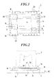
- CMOS image sensor 2 is provided with a light receiving unit 2a which functions as a photoelectric converting device, in approximately central region of the upper surface, and a signal processing circuit 2c in a peripheral region thereof. They are formed in the same semiconductor chip such as a silicon single crystal chip.
- the light receiving unit 2a has a large number of pixels (not shown) which are disposed in two-dimensions. Each pixel comprises a photodiode as a photoelectric conversion element, and a CMOS transistor which performs charge amplification and switching, to generate a signal charge corresponding to received light amount.
- the signal processing circuit 2c comprises a driving circuit for driving the pixels (photoelectric conversion elements) in order, to obtain signal charges, an A/D converter for converting signal charges to digital signals, and a signal processing unit for forming image output signals by using the digital signals, and the like.
- a driving circuit for driving the pixels (photoelectric conversion elements) in order, to obtain signal charges an A/D converter for converting signal charges to digital signals
- a signal processing unit for forming image output signals by using the digital signals, and the like On the periphery of the upper surface of CMOS image sensor 2, in the vicinity of the outer ends of signal processing circuit 2c, a large number of pads 2d are arranged, as shown in FIG. 1.
- CMOS image sensor 2 is adhered to fix at a predetermined position on the substrate PC, as shown in FIG. 2, and is electrically connected to a predetermined circuit on the substrate PC through pads 2d which are terminals for connecting and wires W.
- Color filter array 2f for forming color digital images is provided, and a microlens array 2g is layered on color filter array 2f, as shown in FIG. 2.
- Color filter array 2f and microlens array 2g constitute the first layer.
- Color filter array 2f comprises, for example, red, green and blue filters (three types of primary color filters), which are arranged to correspond to pixels of the light receiving unit 2a, respectively, by a photolithography technique and the like. Color images can be obtained by composing the whole output signals from the pixels.
- Microlens array 2g comprises a plurality of hemisphere-shaped microlenses arranged in two-dimensions and is disposed on light receiving unit 2a through color filter array 2f to correspond to the pixels, respectively, to increase the amount of light entering the photodiodes as photoelectric conversion elements of the pixels.
- Such a microlens array can be fabricated by using a transparent synthetic resin material, a photolithography technique and a technique utilizing the heat fluidity of synthetic resin.
- color filter array 2f and microlens array 2g are formed on the upper surface of light receiving unit 2a, they are also formed on signal processing circuit 2c by the same process at the same time.
- color filter array 2f and microlens array 2g, formed on light receiving unit 2a are kept, the color filter array and the microlens array, of the rest are removed in the production process.
- at least the color filter array and the microlens array on necessary regions (B), even of the rest, are left (the second layer), as described later.
- Such color filter array and microlens array constitute the second layer.
- Abutting portions 1b of a lens supporting member 1 which supports an optical lens abuts onto the upper surface of CMOS image sensor 2.
- the reference numeral 3 denotes an optical lens.
- a certain large abutting area for abutting portions 1 is required.
- the position of light receiving unit 2a of CMOS image sensor 2 is not proper because pixels for converting optical images to signal charges are disposed at the place, and the position of pads 2d in the region of signal processing circuit 2c surrounding light receiving unit 2a is also not proper because wire bonding is performed at the place.
- CMOS image sensor 2 has a structure to enable abutting the abutting portion 1 of lens supporting member 1, in particular, on the upper surface of digital signal processing circuit 2e.
- CMOS image sensor 2 Proper place to be abutted, on the upper surface of CMOS image sensor 2 will be explained more concretely.
- CMOS image sensor 2 In CMOS image sensor 2 according to the embodiment, digital signal processing circuit 2e is arranged in an approximate C-shape when viewing from the top, i.e., region A shown by an alternate long and short dash line in FIG. 1. Therefore, the abutting portion 1b of lens supporting member 1 can be abutted against any place in region A. It is preferable that three, four or more abutting portions 1b are provided, in consideration of keeping a balance of lens supporting member 1 placed on digital signal processing circuit 2e. In the present embodiment shown in the drawings, four abutting portions 1b, like four legs, are provided.
- CMOS image sensor 2 according to the embodiment, four rectangular shaped small regions B shown by an alternate long and two short dashes line in FIG. 1, in which the second layer comprising a color filter array and a microlens array layered thereon, are formed.
- the four abutting portions 1b which are shown by a dash line in FIG. 1, of lens supporting member 1 abut against the second layer in four rectangular shaped small regions B.
- the color filter array and the microlens array layered thereon may be kept to cover almost whole upper surface of the digital signal processing circuit 2e.
- the second layer does not necessarily require both a color filter array and a microlens array layered thereon, on the signal processing circuit.
- the second layer may be constituted with only one of the color filter array and the microlens array.
- the color filter may be constituted by at least one of blue, red and green color filters.
- the color filter array and the microlens array on the upper surface of light receiving unit 2a i.e., as the first layer
- those on the upper surface of the signal processing circuit 2c, i.e., as the second layer is not required to have its inherent optical function.
- lens supporting member 1 can be attached to directly abut to the upper surface of the signal processing circuit 2c of CMOS image sensor, not onto the substrate PC, positioning of lens supporting member 1 with respect to light receiving unit 2a, in the direction of the optical axis can be performed accurately.
- lens supporting member 1 abutting to signal processing circuit 2c of CMOS image sensor 2 can be fastened by pressing lens supporting member 1 down from the top by using an elastic pressing attachment member or the like, through an elastic member such as spring, which gives an appropriate biasing force to lens supporting member 1 in the direction of CMOS image sensor 2, and by engaging to fasten the elastic pressing attachment member to the substrate PC elastically.
- CMOS image sensor 2 electrical connection of CMOS image sensor 2 and the substrate PC is performed by using wires W.
- it can be performed also by wiring through the inside of CMOS image sensor 2 to output signals out of the rear surface or the side surface, of CMOS image sensor 2.
- the image pickup device according to the invention can be incorporated into a digital camera, a cellular phone, a personal computer, a PDA, an audio and visual apparatus, a television, domestic appliances and the like.
Landscapes
- Physics & Mathematics (AREA)
- General Physics & Mathematics (AREA)
- Optics & Photonics (AREA)
- Solid State Image Pick-Up Elements (AREA)
- Transforming Light Signals Into Electric Signals (AREA)
- Steroid Compounds (AREA)
- Nitrogen Condensed Heterocyclic Rings (AREA)
Abstract
Description
Claims (8)
- A CMOS image sensor comprising, a light receiving unit as a photoelectric converting device, and a signal processing circuit; further comprising:a first layer comprising a color filter array and a microlens array layered thereon, which are provided on an upper surface of the light receiving unit; anda second layer comprising at least one of a color filter and a microlens array, provided in a region of at least a portion of an upper surface of the signal processing circuit.
- The CMOS image sensor as claimed in claim 1, wherein the signal processing circuit comprises a digital signal processing circuit and the second layer is formed in a region of an upper surface of the digital signal processing circuit.
- The CMOS image sensor as claimed in claim 1 or 2, wherein the second layer comprises a color filter which comprises one of blue, red and green color filters.
- The CMOS image sensor as claimed in any one of claims 1 to 3, wherein the second layer comprises a structure to enable supporting a lens supporting member for supporting an optical lens, thereon.
- The CMOS image sensor as claimed in any one of the preceding claims, wherein the light receiving unit is formed in an approximate central region of a semiconductor chip and the signal processing circuit is formed in a peripheral region thereof in the same semiconductor chip.
- The CMOS image sensor as claimed in claim 5, wherein the region in which the second layer is provided comprises at least separated three small regions which surround the light receiving unit.
- The CMOS image sensor as claimed in claim 2, wherein the second layer is provided to cover almost whole upper surface of the digital signal processing circuit.
- A CMOS image sensor comprising:a light receiving unit as a photoelectric converting device, comprising a plurality of pixels disposed in two-dimensions, each of which comprises a photoelectric conversion element and a CMOS transistor, to generate a signal charge corresponding to received light amount;a signal processing circuit for processing the signal charge obtained from each of the pixels to form an image signal;a first layer comprising a color filter array and a microlens array layered thereon, which are provided on an upper surface of the light receiving unit; anda second layer comprising at least one of a color filter and a microlens array, provided in a region of at least a portion of an upper surface of the signal processing circuit.
Applications Claiming Priority (2)
| Application Number | Priority Date | Filing Date | Title |
|---|---|---|---|
| JP2001164020 | 2001-05-31 | ||
| JP2001164020 | 2001-05-31 |
Publications (3)
| Publication Number | Publication Date |
|---|---|
| EP1263055A2 true EP1263055A2 (en) | 2002-12-04 |
| EP1263055A3 EP1263055A3 (en) | 2005-03-30 |
| EP1263055B1 EP1263055B1 (en) | 2008-06-11 |
Family
ID=19006887
Family Applications (1)
| Application Number | Title | Priority Date | Filing Date |
|---|---|---|---|
| EP02253569A Expired - Lifetime EP1263055B1 (en) | 2001-05-31 | 2002-05-21 | CMOS image sensor |
Country Status (7)
| Country | Link |
|---|---|
| US (1) | US6727487B2 (en) |
| EP (1) | EP1263055B1 (en) |
| KR (1) | KR100596104B1 (en) |
| CN (1) | CN1226790C (en) |
| AT (1) | ATE398337T1 (en) |
| DE (1) | DE60227027D1 (en) |
| TW (1) | TW540157B (en) |
Cited By (4)
| Publication number | Priority date | Publication date | Assignee | Title |
|---|---|---|---|---|
| FR2860644A1 (en) * | 2003-10-06 | 2005-04-08 | St Microelectronics Sa | COMPONENT, PLATE AND SEMICONDUCTOR HOUSING WITH OPTICAL SENSOR |
| WO2006012866A3 (en) * | 2004-07-28 | 2006-06-22 | Microelectronic Packaging Dres | Image module |
| US7662094B2 (en) | 2002-05-14 | 2010-02-16 | Given Imaging Ltd. | Optical head assembly with dome, and device for use thereof |
| US9320417B2 (en) | 2005-12-29 | 2016-04-26 | Given Imaging Ltd. | In-vivo optical imaging device with backscatter blocking |
Families Citing this family (19)
| Publication number | Priority date | Publication date | Assignee | Title |
|---|---|---|---|---|
| US7323676B2 (en) * | 2001-09-11 | 2008-01-29 | Lumileds Lighting Us, Llc. | Color photosensor with color filters and subtraction unit |
| US6946715B2 (en) * | 2003-02-19 | 2005-09-20 | Micron Technology, Inc. | CMOS image sensor and method of fabrication |
| US20040061799A1 (en) * | 2002-09-27 | 2004-04-01 | Konica Corporation | Image pickup device and portable terminal equipped therewith |
| WO2005020328A1 (en) * | 2003-08-22 | 2005-03-03 | Konica Minolta Opto, Inc. | Solid-state imaging device and imaging device provided with this solid-state imaging device and production method for microlens array of solid-state imaging device |
| US7821564B2 (en) * | 2003-12-30 | 2010-10-26 | Given Imaging Ltd. | Assembly for aligning an optical system |
| US7372497B2 (en) * | 2004-04-28 | 2008-05-13 | Taiwan Semiconductor Manufacturing Company | Effective method to improve sub-micron color filter sensitivity |
| CN1969539A (en) * | 2004-05-04 | 2007-05-23 | 德塞拉股份有限公司 | Compact lens turret assembly |
| US20060109366A1 (en) * | 2004-05-04 | 2006-05-25 | Tessera, Inc. | Compact lens turret assembly |
| JP2005347416A (en) * | 2004-06-01 | 2005-12-15 | Sharp Corp | Solid-state imaging device, semiconductor wafer, and camera module |
| KR100629679B1 (en) | 2004-07-01 | 2006-09-29 | 삼성전자주식회사 | Semiconductor Chip Package With Thermoelectric Cooling Element |
| US7645635B2 (en) * | 2004-08-16 | 2010-01-12 | Micron Technology, Inc. | Frame structure and semiconductor attach process for use therewith for fabrication of image sensor packages and the like, and resulting packages |
| KR100868630B1 (en) * | 2006-12-11 | 2008-11-13 | 동부일렉트로닉스 주식회사 | Pattern mask for forming microlens, image sensor and manufacturing method thereof |
| US20090283665A1 (en) * | 2008-05-13 | 2009-11-19 | Eastman Kodak Company | Image sensor with an aligned optical assembly |
| JP5553707B2 (en) * | 2009-08-21 | 2014-07-16 | 株式会社半導体エネルギー研究所 | Photodetector |
| US8461567B2 (en) * | 2010-06-24 | 2013-06-11 | Nokia Corporation | Apparatus and method for sensing photons |
| JP2014123014A (en) * | 2012-12-21 | 2014-07-03 | Casio Comput Co Ltd | Light source device, projector |
| US9917991B2 (en) * | 2014-10-24 | 2018-03-13 | Apple Inc. | Camera actuator |
| TWI613478B (en) * | 2016-09-12 | 2018-02-01 | 台睿精工股份有限公司 | Structure of single-lens with mechanic zero tile angle and adjustment method thereof |
| CN109115250A (en) * | 2018-08-08 | 2019-01-01 | 珠海格力电器股份有限公司 | Array structure of photosensitive device and photoelectric encoder |
Family Cites Families (12)
| Publication number | Priority date | Publication date | Assignee | Title |
|---|---|---|---|---|
| US5321249A (en) * | 1991-10-31 | 1994-06-14 | Matsushita Electric Industrial Co., Ltd. | Solid-state imaging device and method of manufacturing the same |
| KR950002410A (en) * | 1993-06-30 | 1995-01-04 | 김광호 | Solid-state imaging device |
| JPH10270672A (en) * | 1997-03-25 | 1998-10-09 | Sony Corp | Solid-state imaging device |
| EP0948059A1 (en) * | 1998-02-05 | 1999-10-06 | Asulab S.A. | Positioning means in a microelectronic device and imaging device using the same |
| KR20000050478A (en) * | 1999-01-11 | 2000-08-05 | 윤종용 | CCD image sensor module and manufacturing method thereof |
| US6137634A (en) * | 1999-02-01 | 2000-10-24 | Intel Corporation | Microlens array |
| KR100359768B1 (en) * | 1999-03-18 | 2002-11-07 | 주식회사 하이닉스반도체 | Solid state image sensor and method for fabricating the same |
| FR2798226B1 (en) * | 1999-09-02 | 2002-04-05 | St Microelectronics Sa | METHOD FOR PACKAGING A SEMICONDUCTOR CHIP CONTAINING SENSORS AND PACKAGE OBTAINED |
| US6171885B1 (en) * | 1999-10-12 | 2001-01-09 | Taiwan Semiconductor Manufacturing Company | High efficiency color filter process for semiconductor array imaging devices |
| JP3840058B2 (en) * | 2000-04-07 | 2006-11-01 | キヤノン株式会社 | Microlens, solid-state imaging device and manufacturing method thereof |
| US6395576B1 (en) * | 2000-06-14 | 2002-05-28 | Taiwan Semiconductor Manufacturing Company | High efficiency color filter process to improve color balance in semiconductor array imaging devices |
| TW523924B (en) * | 2001-01-12 | 2003-03-11 | Konishiroku Photo Ind | Image pickup device and image pickup lens |
-
2002
- 2002-05-20 TW TW091110530A patent/TW540157B/en not_active IP Right Cessation
- 2002-05-21 EP EP02253569A patent/EP1263055B1/en not_active Expired - Lifetime
- 2002-05-21 DE DE60227027T patent/DE60227027D1/en not_active Expired - Lifetime
- 2002-05-21 AT AT02253569T patent/ATE398337T1/en not_active IP Right Cessation
- 2002-05-22 CN CNB021202958A patent/CN1226790C/en not_active Expired - Lifetime
- 2002-05-28 KR KR1020020029553A patent/KR100596104B1/en not_active Expired - Lifetime
- 2002-05-29 US US10/156,017 patent/US6727487B2/en not_active Expired - Lifetime
Cited By (4)
| Publication number | Priority date | Publication date | Assignee | Title |
|---|---|---|---|---|
| US7662094B2 (en) | 2002-05-14 | 2010-02-16 | Given Imaging Ltd. | Optical head assembly with dome, and device for use thereof |
| FR2860644A1 (en) * | 2003-10-06 | 2005-04-08 | St Microelectronics Sa | COMPONENT, PLATE AND SEMICONDUCTOR HOUSING WITH OPTICAL SENSOR |
| WO2006012866A3 (en) * | 2004-07-28 | 2006-06-22 | Microelectronic Packaging Dres | Image module |
| US9320417B2 (en) | 2005-12-29 | 2016-04-26 | Given Imaging Ltd. | In-vivo optical imaging device with backscatter blocking |
Also Published As
| Publication number | Publication date |
|---|---|
| ATE398337T1 (en) | 2008-07-15 |
| EP1263055A3 (en) | 2005-03-30 |
| KR100596104B1 (en) | 2006-07-05 |
| CN1389928A (en) | 2003-01-08 |
| TW540157B (en) | 2003-07-01 |
| EP1263055B1 (en) | 2008-06-11 |
| KR20020091792A (en) | 2002-12-06 |
| US20020195546A1 (en) | 2002-12-26 |
| DE60227027D1 (en) | 2008-07-24 |
| US6727487B2 (en) | 2004-04-27 |
| CN1226790C (en) | 2005-11-09 |
Similar Documents
| Publication | Publication Date | Title |
|---|---|---|
| US6727487B2 (en) | CMOS image sensor | |
| TWI236284B (en) | Camera module and manufacturing method thereof | |
| US8107005B2 (en) | Method of manufacturing an image sensor module | |
| CN108206907B (en) | Array camera module and electronic equipment | |
| US9070610B2 (en) | Solid-state imaging device and electronic apparatus | |
| US20110285890A1 (en) | Camera module | |
| WO2001065839A1 (en) | Small-sized image pickup module | |
| JP2004080039A (en) | CMOS image sensor structure and process for manufacturing camera module using the same | |
| CN101304037A (en) | Image capturing device module, manufacturing method thereof, and electronic information device | |
| US20030146998A1 (en) | Small-size imaging apparatus, in particular photographic appliance or camera | |
| KR100816844B1 (en) | Image sensor module and manufacturing method thereof and camera module including same | |
| JP4720120B2 (en) | Semiconductor image sensor module | |
| JP4929553B2 (en) | Camera module and manufacturing method thereof | |
| KR102899367B1 (en) | Camera module | |
| US7329055B2 (en) | Optoelectronics processing module and method for manufacturing thereof | |
| KR100992338B1 (en) | Camera module | |
| JP4907034B2 (en) | CMOS image sensor | |
| US8049809B2 (en) | Solid-state image pickup device and electronic instruments | |
| US7009287B2 (en) | Chip on photosensitive device package structure and electrical connection thereof | |
| KR20080081726A (en) | Image sensor module and camera module having same | |
| KR101184906B1 (en) | Dual camera module, portable terminal with the same and manufacturing method thereof | |
| JP4961393B2 (en) | Solid-state imaging device and method for manufacturing solid-state imaging device | |
| US7479397B2 (en) | Optoelectronics processing module and method for manufacturing thereof | |
| JP2011077555A (en) | Semiconductor image sensor module, and method of manufacturing semiconductor image sensor module | |
| KR101607212B1 (en) | camera module |
Legal Events
| Date | Code | Title | Description |
|---|---|---|---|
| PUAI | Public reference made under article 153(3) epc to a published international application that has entered the european phase |
Free format text: ORIGINAL CODE: 0009012 |
|
| AK | Designated contracting states |
Kind code of ref document: A2 Designated state(s): AT BE CH CY DE DK ES FI FR GB GR IE IT LI LU MC NL PT SE TR |
|
| AX | Request for extension of the european patent |
Free format text: AL;LT;LV;MK;RO;SI |
|
| PUAL | Search report despatched |
Free format text: ORIGINAL CODE: 0009013 |
|
| AK | Designated contracting states |
Kind code of ref document: A3 Designated state(s): AT BE CH CY DE DK ES FI FR GB GR IE IT LI LU MC NL PT SE TR |
|
| AX | Request for extension of the european patent |
Extension state: AL LT LV MK RO SI |
|
| 17P | Request for examination filed |
Effective date: 20050527 |
|
| RAP1 | Party data changed (applicant data changed or rights of an application transferred) |
Owner name: KONICA MINOLTA OPTO, INC. Owner name: HYNIX SEMICONDUCTOR INC. |
|
| AKX | Designation fees paid |
Designated state(s): AT BE CH CY DE DK ES FI FR GB GR IE IT LI LU MC NL PT SE TR |
|
| AXX | Extension fees paid |
Extension state: LT Payment date: 20050527 Extension state: AL Payment date: 20050527 Extension state: LV Payment date: 20050527 Extension state: MK Payment date: 20050527 Extension state: SI Payment date: 20050527 Extension state: RO Payment date: 20050527 |
|
| RAP1 | Party data changed (applicant data changed or rights of an application transferred) |
Owner name: MAGNA CHIP SEMICONDUCTOR, LTD. Owner name: KONICA MINOLTA OPTO, INC. |
|
| 17Q | First examination report despatched |
Effective date: 20070118 |
|
| GRAP | Despatch of communication of intention to grant a patent |
Free format text: ORIGINAL CODE: EPIDOSNIGR1 |
|
| RIC1 | Information provided on ipc code assigned before grant |
Ipc: H01L 31/0232 20060101ALI20070921BHEP Ipc: H01L 27/146 20060101ALI20070921BHEP Ipc: H01L 31/0203 20060101AFI20070921BHEP |
|
| GRAS | Grant fee paid |
Free format text: ORIGINAL CODE: EPIDOSNIGR3 |
|
| GRAA | (expected) grant |
Free format text: ORIGINAL CODE: 0009210 |
|
| AK | Designated contracting states |
Kind code of ref document: B1 Designated state(s): AT BE CH CY DE DK ES FI FR GB GR IE IT LI LU MC NL PT SE TR |
|
| AX | Request for extension of the european patent |
Extension state: AL LT LV MK RO SI |
|
| REG | Reference to a national code |
Ref country code: GB Ref legal event code: FG4D |
|
| REG | Reference to a national code |
Ref country code: CH Ref legal event code: EP |
|
| REF | Corresponds to: |
Ref document number: 60227027 Country of ref document: DE Date of ref document: 20080724 Kind code of ref document: P |
|
| REG | Reference to a national code |
Ref country code: IE Ref legal event code: FG4D |
|
| PG25 | Lapsed in a contracting state [announced via postgrant information from national office to epo] |
Ref country code: NL Free format text: LAPSE BECAUSE OF FAILURE TO SUBMIT A TRANSLATION OF THE DESCRIPTION OR TO PAY THE FEE WITHIN THE PRESCRIBED TIME-LIMIT Effective date: 20080611 Ref country code: AT Free format text: LAPSE BECAUSE OF FAILURE TO SUBMIT A TRANSLATION OF THE DESCRIPTION OR TO PAY THE FEE WITHIN THE PRESCRIBED TIME-LIMIT Effective date: 20080611 |
|
| NLV1 | Nl: lapsed or annulled due to failure to fulfill the requirements of art. 29p and 29m of the patents act | ||
| PG25 | Lapsed in a contracting state [announced via postgrant information from national office to epo] |
Ref country code: SE Free format text: LAPSE BECAUSE OF FAILURE TO SUBMIT A TRANSLATION OF THE DESCRIPTION OR TO PAY THE FEE WITHIN THE PRESCRIBED TIME-LIMIT Effective date: 20080911 Ref country code: ES Free format text: LAPSE BECAUSE OF FAILURE TO SUBMIT A TRANSLATION OF THE DESCRIPTION OR TO PAY THE FEE WITHIN THE PRESCRIBED TIME-LIMIT Effective date: 20080922 Ref country code: PT Free format text: LAPSE BECAUSE OF FAILURE TO SUBMIT A TRANSLATION OF THE DESCRIPTION OR TO PAY THE FEE WITHIN THE PRESCRIBED TIME-LIMIT Effective date: 20081111 |
|
| PG25 | Lapsed in a contracting state [announced via postgrant information from national office to epo] |
Ref country code: BE Free format text: LAPSE BECAUSE OF FAILURE TO SUBMIT A TRANSLATION OF THE DESCRIPTION OR TO PAY THE FEE WITHIN THE PRESCRIBED TIME-LIMIT Effective date: 20080611 |
|
| PLBE | No opposition filed within time limit |
Free format text: ORIGINAL CODE: 0009261 |
|
| STAA | Information on the status of an ep patent application or granted ep patent |
Free format text: STATUS: NO OPPOSITION FILED WITHIN TIME LIMIT |
|
| PG25 | Lapsed in a contracting state [announced via postgrant information from national office to epo] |
Ref country code: DK Free format text: LAPSE BECAUSE OF FAILURE TO SUBMIT A TRANSLATION OF THE DESCRIPTION OR TO PAY THE FEE WITHIN THE PRESCRIBED TIME-LIMIT Effective date: 20080611 |
|
| 26N | No opposition filed |
Effective date: 20090312 |
|
| PG25 | Lapsed in a contracting state [announced via postgrant information from national office to epo] |
Ref country code: IT Free format text: LAPSE BECAUSE OF FAILURE TO SUBMIT A TRANSLATION OF THE DESCRIPTION OR TO PAY THE FEE WITHIN THE PRESCRIBED TIME-LIMIT Effective date: 20080611 |
|
| PGFP | Annual fee paid to national office [announced via postgrant information from national office to epo] |
Ref country code: FI Payment date: 20090515 Year of fee payment: 8 |
|
| PG25 | Lapsed in a contracting state [announced via postgrant information from national office to epo] |
Ref country code: MC Free format text: LAPSE BECAUSE OF NON-PAYMENT OF DUE FEES Effective date: 20090531 |
|
| REG | Reference to a national code |
Ref country code: CH Ref legal event code: PL |
|
| PG25 | Lapsed in a contracting state [announced via postgrant information from national office to epo] |
Ref country code: CH Free format text: LAPSE BECAUSE OF NON-PAYMENT OF DUE FEES Effective date: 20090531 Ref country code: LI Free format text: LAPSE BECAUSE OF NON-PAYMENT OF DUE FEES Effective date: 20090531 |
|
| REG | Reference to a national code |
Ref country code: FR Ref legal event code: ST Effective date: 20100129 |
|
| PG25 | Lapsed in a contracting state [announced via postgrant information from national office to epo] |
Ref country code: FR Free format text: LAPSE BECAUSE OF NON-PAYMENT OF DUE FEES Effective date: 20090602 Ref country code: IE Free format text: LAPSE BECAUSE OF NON-PAYMENT OF DUE FEES Effective date: 20090521 |
|
| REG | Reference to a national code |
Ref country code: FR Ref legal event code: RN |
|
| REG | Reference to a national code |
Ref country code: FR Ref legal event code: FC |
|
| PG25 | Lapsed in a contracting state [announced via postgrant information from national office to epo] |
Ref country code: GR Free format text: LAPSE BECAUSE OF FAILURE TO SUBMIT A TRANSLATION OF THE DESCRIPTION OR TO PAY THE FEE WITHIN THE PRESCRIBED TIME-LIMIT Effective date: 20080912 |
|
| PGRI | Patent reinstated in contracting state [announced from national office to epo] |
Ref country code: FR Effective date: 20100913 |
|
| PG25 | Lapsed in a contracting state [announced via postgrant information from national office to epo] |
Ref country code: FI Free format text: LAPSE BECAUSE OF NON-PAYMENT OF DUE FEES Effective date: 20100521 |
|
| PG25 | Lapsed in a contracting state [announced via postgrant information from national office to epo] |
Ref country code: LU Free format text: LAPSE BECAUSE OF NON-PAYMENT OF DUE FEES Effective date: 20090521 |
|
| PGFP | Annual fee paid to national office [announced via postgrant information from national office to epo] |
Ref country code: FR Payment date: 20110523 Year of fee payment: 10 |
|
| PG25 | Lapsed in a contracting state [announced via postgrant information from national office to epo] |
Ref country code: TR Free format text: LAPSE BECAUSE OF FAILURE TO SUBMIT A TRANSLATION OF THE DESCRIPTION OR TO PAY THE FEE WITHIN THE PRESCRIBED TIME-LIMIT Effective date: 20080611 |
|
| PGFP | Annual fee paid to national office [announced via postgrant information from national office to epo] |
Ref country code: GB Payment date: 20110518 Year of fee payment: 10 |
|
| PG25 | Lapsed in a contracting state [announced via postgrant information from national office to epo] |
Ref country code: CY Free format text: LAPSE BECAUSE OF FAILURE TO SUBMIT A TRANSLATION OF THE DESCRIPTION OR TO PAY THE FEE WITHIN THE PRESCRIBED TIME-LIMIT Effective date: 20080611 |
|
| PGFP | Annual fee paid to national office [announced via postgrant information from national office to epo] |
Ref country code: DE Payment date: 20110518 Year of fee payment: 10 |
|
| GBPC | Gb: european patent ceased through non-payment of renewal fee |
Effective date: 20120521 |
|
| REG | Reference to a national code |
Ref country code: FR Ref legal event code: ST Effective date: 20130131 |
|
| REG | Reference to a national code |
Ref country code: DE Ref legal event code: R119 Ref document number: 60227027 Country of ref document: DE Effective date: 20121201 |
|
| PG25 | Lapsed in a contracting state [announced via postgrant information from national office to epo] |
Ref country code: GB Free format text: LAPSE BECAUSE OF NON-PAYMENT OF DUE FEES Effective date: 20120521 Ref country code: FR Free format text: LAPSE BECAUSE OF NON-PAYMENT OF DUE FEES Effective date: 20120531 |
|
| PG25 | Lapsed in a contracting state [announced via postgrant information from national office to epo] |
Ref country code: DE Free format text: LAPSE BECAUSE OF NON-PAYMENT OF DUE FEES Effective date: 20121201 |