EP1261012A2 - Flat panel type display apparatus - Google Patents
Flat panel type display apparatus Download PDFInfo
- Publication number
- EP1261012A2 EP1261012A2 EP02011373A EP02011373A EP1261012A2 EP 1261012 A2 EP1261012 A2 EP 1261012A2 EP 02011373 A EP02011373 A EP 02011373A EP 02011373 A EP02011373 A EP 02011373A EP 1261012 A2 EP1261012 A2 EP 1261012A2
- Authority
- EP
- European Patent Office
- Prior art keywords
- tape
- driving
- flexible wiring
- grounding
- flat panel
- Prior art date
- Legal status (The legal status is an assumption and is not a legal conclusion. Google has not performed a legal analysis and makes no representation as to the accuracy of the status listed.)
- Granted
Links
Images



Classifications
-
- H—ELECTRICITY
- H05—ELECTRIC TECHNIQUES NOT OTHERWISE PROVIDED FOR
- H05K—PRINTED CIRCUITS; CASINGS OR CONSTRUCTIONAL DETAILS OF ELECTRIC APPARATUS; MANUFACTURE OF ASSEMBLAGES OF ELECTRICAL COMPONENTS
- H05K7/00—Constructional details common to different types of electric apparatus
- H05K7/20—Modifications to facilitate cooling, ventilating, or heating
- H05K7/20954—Modifications to facilitate cooling, ventilating, or heating for display panels
- H05K7/20963—Heat transfer by conduction from internal heat source to heat radiating structure
-
- H—ELECTRICITY
- H01—ELECTRIC ELEMENTS
- H01J—ELECTRIC DISCHARGE TUBES OR DISCHARGE LAMPS
- H01J2217/00—Gas-filled discharge tubes
- H01J2217/38—Cold-cathode tubes
- H01J2217/49—Display panels, e.g. not making use of alternating current
- H01J2217/492—Details
Definitions
- the present invention relates to a flat panel type display apparatus such as a plasma display panel (hereinafter referred to as PDP) or the like, and more particularly to a mounting structure of a integrated circuit device for driving the flat panel type display apparatus.
- a flat panel type display apparatus such as a plasma display panel (hereinafter referred to as PDP) or the like
- PDP plasma display panel
- driving ICs integrated circuit devices for driving
- the TCP(tape carrier package) for mounting the driving IC using a mounting technology such as, for example, TAB (tape automated bonding), COF (chip on FPC), or the like, is used for connecting the driving IC with electrode terminals formed on a substrate of a flat display panel such as the PDP.
- TAB tape automated bonding
- COF chip on FPC
- an object of the present invention is to solve such problems, and more particularly to provide a flat panel type display apparatus having a mounting structure for a driving IC capable of obtaining the superior heat radiation and withstand voltage characteristic, and realizing a simpler structure and lower production cost.
- the present invention provides a flat panel type display apparatus, comprising a flat display body, a metal chassis for supporting the display body at a back surface thereof, a flexible wiring tape electrically connected with the display body, having predetermined wiring patterns including a grounding wiring pattern formed thereon, driving ICs mounted on the flexible wiring tape, and a thermally and electrically conductive tape, wherein a rear surface of each driving IC is connected with the grounding pattern formed on the flexible wiring tape through the conductive tape.
- the rear surface of the driving IC mounted on the flexible wiring tape is connected with the grounding pattern through the conductive tape, so that the rear surface of the driving IC can be surely grounded.
- the withstand voltage characteristic can be improved.
- the heat generated when the flat display panel is driven to be displayed by the driving IC can be effectively radiated by a heat radiation function of the conductive tape. Since these effects can be produced by a simpler mounting structure with the conductive tape, the mounting density of the driving ICs having a high voltage and a high electric power can be improved.
- the conductive tape is an adhesive tape with an adhesive layer provided upon a surface thereof, which is adhered upon the rear surface of driving IC and a surface of the grounding pattern.
- connection between the rear surface of the driving IC and the surface of the grounding pattern is completed just through adhering the conductive adhesive tape, so that the workhours of mounting step can be shortened, and a production cost also can be reduced.
- the conductive tape is a double-surfaces adhesive tape having adhesive layers on both sides thereof, one surface being adhered onto the driving ICs and the grounding pattern, and also another being adhered onto the metal chassis.
- the driving ICs can be easily fixed onto the metal chassis, so that the stability of the driving IC to be mounted increases.
- the driving IC's contact with the metal chassis can improve the function of heat radiation.
- the flexible wiring tape has a plurality of apertures thereon, and the driving ICs are connected with the wiring patterns formed on an outside surface of the flexible wiring tape by metal lead members passing through the apertures.
- the conductive tape is adhered upon a surface opposite to a wiring pattern forming surface on the flexible wiring tape, so that a short circuit generated between the wiring pattern and the conductive tape can be prevented. As a result, it results in allowing a large area of conductive tape to be attached, thereby further improving the effect of heat radiation.
- FIG. 1 is a sectional view illustrating a longitudinal sectional structure of a critical portion of the color plasma display panel
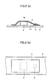
- Figs. 2(a) and 2(b) are schematic views illustrating a mounting structure using a flexible wiring tape.
- the color plasma display panel 1 comprises a display body 2, a metal chassis 3 for supporting the display body 2, wherein a driving IC 9(silicon chip, semiconductor chip) and the like are wired by a flexible wiring tape 8 to be mounted on a back side of the metal chassis 3 as well as a printed board 12.
- a driving IC 9 silicon chip, semiconductor chip
- the display body 2 having a flat shape, comprises a front glass substrate 4 and a back glass substrate 5 arranged opposing each other with a discharge space having a rare gas sealed therein interposed therebetween.
- a multiplicity of row electrode pairs covered by dielectric layers are regularly arranged
- a multiplicity of column electrodes covered by fluorescent material layers of respective colors are orthogonally arranged in relation to the row electrode pairs.
- Respective intersections of the row electrode pairs and the column electrodes operate as color discharge cells.
- the driving IC 9 supplies driving power for displaying to the row electrode pairs and column electrodes based on display data, the color discharge cells are discharged to be illuminated, thereby a color image is displayed.
- the flat display body 2 is fixed to the flat metal chassis 3 formed of aluminum or the like by an adhesive material 6 such as a double-sides adhesive tape and is integrated therewith.
- Draw-out terminals (hereinafter referred to as column electrode terminals) connected with the column electrodes are formed in alignment at a side edge 7 of the front surface of the back glass substrate 5, and draw-out terminals (hereinafter referred to as row electrode terminals) connected with the row electrode pairs are formed in alignment also at a side edge (not shown) of the back surface of the front glass substrate 4.
- Wiring patterns for predetermined signal transmission are previously formed in addition to grounding wiring patterns and power source wiring patterns on the flexible wiring tape 8, and a driving IC module(TCP), which is the flexible wiring tape 8 previously provided with the driving IC 9, is formed by electrically connecting one or more driving ICs 9 to these wiring patterns.
- a driving IC module(TCP) which is the flexible wiring tape 8 previously provided with the driving IC 9
- an edge 8a of the flexible wiring tape 8 composing the module is fixed to the side edge 7 of the back glass substrate 5 and the above-described side edge of the front glass substrate 4, and then a predetermined connecting edges of the wiring patterns formed at the edge 8a of the flexible wiring tape 8 are electrically connected with the column electrode terminals and row electrode terminals through an anisotropic conductive adhesive sheet or the like.
- the driving IC module and the display body 2 are electrically connected with each other.
- a connecting structure between the side edge of the front glass substrate 4 and the wiring tape 8 is not shown in Fig. 1.
- the driving IC module is formed in the following way.
- the predetermined wiring patterns as mentioned above are previously formed on the flexible wiring tape 8, so that the flexible wiring tape 8 capable of conducting TAB(Tape Automated Bonding) can be obtained.
- the driving IC 9 When the driving IC 9 is mounted on the flexible wiring tape 8, the driving IC 9 is positioned and disposed in relation to the flexible wiring tape 8, while automatically carrying the flexible wiring tape 8, by an automatic mounting machine. Then, a side of bonding pad or electric circuit surface formed on the driving IC 9 is contacted to the wiring patterns of the flexible wiring tape 8, while a rear surface 9a of the driving IC 9 is disposed facing upward in relation to the flexible wiring tape 8.
- a metal plate film of chromium and gold is formed.
- the metal plate film is formed by plating chromium and gold after removing a oxide film of the rear surface through grinding it by a grinder.
- an electrically conductive tape 11 having an adhesive material layer 11a is adhered onto a surface of a grounding wiring pattern 10, which is formed on the flexible wiring tape 8, and also onto the rear surface 9a of each driving IC 9, which becomes electrically conductive condition by the plating treatment as mentioned above, respectively, as a result of which the driving IC 9 is connected with the grounding wiring pattern 10 through the conductive tape 11.
- the driving IC module capable of efficiently radiating the heat generated by the driving ICs 9 through the conductive tape 11, and also capable of sufficiently stabilizing a ground potential of the driving ICs 9.
- the edge 8a of the flexible wiring tape 8 is fixed to the side edge 7 of the back glass substrate 5 and the above-described side edge of the front glass substrate 4 when the driving IC module as mentioned above is mounted on the display body 2 and the metal chassis 3 as shown in Fig. 1. Then, the predetermined connecting edges of the wiring patterns formed at the edge 8a of the flexible wiring tape 8 are electrically connected with the column electrode terminals and row electrode terminals through the anisotropic conductive adhesive sheet(not shown) or the like.
- the tape 11 When adhering the conductive tape 11 to the back surface of the metal chassis 3 like this, the tape 11 may be a conductive tape capable of adhering the both sides thereof, which has adhesive layers provided with the electrical conductivity and a high heat conductivity upon the both sides, so that the adhering work can be rapidly completed.
- the heat generated at the side of the driving IC when the display body 2 is driven by the driving IC 9 is efficiently conducted to the conductive tape 11, thus the heat radiation of the apparatus can be improved by employing the conductive tape 11 having a wide surface area and the heat conductivity (see Fig. 2(b)). Additionally, since the conductive tape 11 is adhered to the metal chassis 3, the heat radiation of the metal chassis 3 also is accomplished. In a word, according to the present invention, an extremely preferable effect of heat radiation can be obtained.
- the rear surface 9a(metal chassis side) of the driving IC 9 which is subject to a conductive treatment, is connected to the grounding wiring pattern 10 through the conductive tape 11, so that a ground potential of the driving IC 9 can be kept with the same potential as that of the grounding wiring pattern 10 of the flexible wiring tape 8. As a result, a withstand voltage characteristic can be improved.
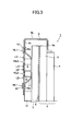
- Fig. 3 is a longitudinal sectional view of a critical portion illustrating another embodiment of the present invention. It should be noted that, in Fig. 3, equivalent portions with those in Fig. 1 are designated by the same reference numerals.
- a main difference in a structure of the flat panel type display apparatus as shown in Fig. 3 from that shown in Fig. 1 is that a wiring pattern forming surface 8b of the flexible wiring tape 8 is provided on an outside surface of the tape 8 so as to prevent the wiring pattern formed on the tape 8 from interfering with the conductive tape 11.
- the grounding wiring patterns 10 formed on the wiring pattern forming surface 8b of the flexible wiring tape 8 has electrodes 10a to be exposed on a surface 8c opposing to the wiring pattern forming surface 8b through one or more apertures HL1 formed on the flexible wiring tape 8.
- the electrodes 10a are connected with each rear surface of the driving ICs 9 through the conductive tape 11.
- the driving ICs 9 are connected with the wiring patterns provided on the wiring pattern forming surface 8b of the flexible wiring tape 8 by one or a plurality of metal lead members LD through one or a plurality of apertures HL2 formed on the flexible wiring tape 8.
- the large size of conductive tape 11 can be mounted while previously preventing short circuit (electrical short circuit) against the wiring patterns by directly mounting the conductive tape 11 on the surface 8c opposite to the wiring pattern forming surface 8b of the flexible wiring tape 8, and also a plurality of apertures HL1, HL2 are provided on the flexible wiring tape 8, thus the heat radiation effect of the driving ICs 9 can be further improved.
- a connecting portion between the driving IC 9 and the flexible wiring tape 8 may be covered with a resin 13.
- the grounding wiring pattern 10, which is formed on the wiring pattern forming surface 8b of the flexible wiring tape 8 may be connected with the conductive tape 11 disposed on the opposite surface 8c through the apertures HL1 in the same drawing.
- Figs. 5(a) and 5(b) are explanatory views showing modified examples corresponding to a various kind of metal chassis formation.
- an auxiliary chassis 3a to enclose respective upper portions of both the display body 2 and the metal chassis 3 may be fixed with the metal chassis 3, an inside surface of the auxiliary chassis 3a being adhered with an outside surface of the conductive tape 11, which is a surface opposing to a surface adhered upon the driving IC 9, as shown in Fig. 5(a).
- Fig. 5(a) is explanatory views showing modified examples corresponding to a various kind of metal chassis formation.
- 5(b) discloses the metal chassis 3 having a bent portion formed upon an end of the metal chassis 3, where the driving IC module is introduced through an aperture provided on the bent portion 3b, and then the bent portion 3b may be adhered to the outside surface of the conductive tape 11 as well as that of Fig. 5(a).
- each rear surface 9a of the driving ICs 9 provided on the flexible wiring tape 8 is connected with the grounding wiring pattern 10 through the conductive tape 11.
- the rear surface 9a of the driving IC 9 can be surely grounded, as a result of which the withstand voltage characteristic can be improved based on a shield effect.
- the heat generated when the color plasma display panel is driven by the driving IC 9 can be effectively radiated by a heat radiation function of the conductive tape 11. Since both the heat radiation and withstand voltage characteristics can be improved by the simple mounting structure, a mounting density of the driving ICs and the like can be improved.
- connection step can be completed in the same process as the mounting of the driving IC and the grounding wiring pattern, thus the production cost of the apparatus can be reduced because of the simple manufacturing step.
Landscapes
- Physics & Mathematics (AREA)
- Thermal Sciences (AREA)
- Engineering & Computer Science (AREA)
- Microelectronics & Electronic Packaging (AREA)
- Devices For Indicating Variable Information By Combining Individual Elements (AREA)
Abstract
Description
Claims (7)
- A flat panel type display apparatus (1), comprising:wherein a rear surface of the each of the driving ICs (9) is connected with the grounding wiring pattern (10) formed on the flexible wiring tape (8) through the conductive tape (11).a flat display body (2);a metal chassis (3) for supporting the display body at a back surface thereof;a flexible wiring tape (8) electrically connected with the display body, having predetermined wiring patterns including a grounding wiring pattern (10) formed thereon;driving ICs (9) mounted on the flexible wiring tape (8); anda thermally and electrically conductive tape (11),
- The apparatus according to claim 1,
wherein the conductive tape (11) is an adhesive tape with an adhesive layer (11a) on a surface thereof, which is adhered upon the rear surface (9a) of each driving IC (9) and a surface of the grounding pattern (10). - The apparatus according to claim 1,
wherein the conductive tape (11) is a double-surface adhesive tape having adhesive layers on both sides thereof, one surface being adhered onto the driving IC (9) and the grounding pattern (10), and another surface being adhered onto the metal chassis (3). - The apparatus according to any of claims 1 to 3,
wherein the driving ICs (9) are semiconductor integrated circuit devices. - The apparatus according to any of claims 1 to 4,
wherein the flexible wiring tape (8) has printed thereon wiring patterns for grounding, power source and signal transmission. - The apparatus according to any of claims 1 to 5,
wherein the flexible wiring tape (8) has a plurality of apertures (HL1, HL2) therein, and wherein the driving ICs (9) are connected with the wiring patterns formed on an outside surface of the flexible wiring tape (8) by metal lead members (LD) passing through the apertures (HL1, HL2). - The apparatus according to any of claims 1 to 6,
wherein the flat panel type display apparatus is a color plasma display panel.
Applications Claiming Priority (2)
| Application Number | Priority Date | Filing Date | Title |
|---|---|---|---|
| JP2001155152A JP4650822B2 (en) | 2001-05-24 | 2001-05-24 | Flat panel display |
| JP2001155152 | 2001-05-24 |
Publications (3)
| Publication Number | Publication Date |
|---|---|
| EP1261012A2 true EP1261012A2 (en) | 2002-11-27 |
| EP1261012A3 EP1261012A3 (en) | 2005-04-13 |
| EP1261012B1 EP1261012B1 (en) | 2007-07-11 |
Family
ID=18999392
Family Applications (1)
| Application Number | Title | Priority Date | Filing Date |
|---|---|---|---|
| EP02011373A Expired - Lifetime EP1261012B1 (en) | 2001-05-24 | 2002-05-23 | Flat panel type display apparatus |
Country Status (4)
| Country | Link |
|---|---|
| US (1) | US6534722B2 (en) |
| EP (1) | EP1261012B1 (en) |
| JP (1) | JP4650822B2 (en) |
| DE (1) | DE60221071T2 (en) |
Cited By (2)
| Publication number | Priority date | Publication date | Assignee | Title |
|---|---|---|---|---|
| CN100361172C (en) * | 2004-09-03 | 2008-01-09 | Lg电子株式会社 | Plasma display apparatus including heat sink assembly apparatus |
| EP1699066A3 (en) * | 2005-03-03 | 2009-12-09 | LG Electronics Inc. | Display apparatus and flexible substrate |
Families Citing this family (55)
| Publication number | Priority date | Publication date | Assignee | Title |
|---|---|---|---|---|
| US6885004B2 (en) * | 1997-11-28 | 2005-04-26 | Nanocrystal Imaging Corporation | High resolution tiled microchannel storage phosphor based radiation sensor |
| JP2004271611A (en) | 2003-03-05 | 2004-09-30 | Pioneer Electronic Corp | Flat panel display apparatus |
| JP3996535B2 (en) * | 2003-03-20 | 2007-10-24 | Nec液晶テクノロジー株式会社 | Liquid crystal display |
| WO2005022493A1 (en) | 2003-08-29 | 2005-03-10 | Matsushita Electric Industrial Co., Ltd. | Plasma display device |
| US20050088092A1 (en) * | 2003-10-17 | 2005-04-28 | Myoung-Kon Kim | Plasma display apparatus |
| KR100570645B1 (en) | 2003-10-23 | 2006-04-12 | 삼성에스디아이 주식회사 | Plasma display device with driver IC heat dissipation |
| KR100627381B1 (en) * | 2003-10-23 | 2006-09-22 | 삼성에스디아이 주식회사 | Plasma display device with driver IC heat dissipation |
| KR100669696B1 (en) | 2003-11-08 | 2007-01-16 | 삼성에스디아이 주식회사 | Plasma display |
| KR100627384B1 (en) | 2003-11-11 | 2006-09-21 | 삼성에스디아이 주식회사 | Plasma display device with driver IC heat dissipation structure |
| KR100603322B1 (en) * | 2003-11-29 | 2006-07-20 | 삼성에스디아이 주식회사 | Plasma display |
| KR100683746B1 (en) | 2004-12-30 | 2007-02-15 | 삼성에스디아이 주식회사 | Chassis assembly for plasma display device and plasma display panel having same |
| KR100637149B1 (en) * | 2004-02-20 | 2006-10-20 | 삼성에스디아이 주식회사 | Plasma display device |
| US7508673B2 (en) * | 2004-03-04 | 2009-03-24 | Samsung Sdi Co., Ltd. | Heat dissipating apparatus for plasma display device |
| JP2005331945A (en) * | 2004-05-18 | 2005-12-02 | Samsung Sdi Co Ltd | Plasma display device |
| KR100669409B1 (en) * | 2004-05-20 | 2007-01-15 | 삼성에스디아이 주식회사 | Plasma display device with driver IC heat dissipation structure |
| KR100669376B1 (en) * | 2004-05-28 | 2007-01-15 | 삼성에스디아이 주식회사 | Plasma display device |
| US6972963B1 (en) * | 2004-07-02 | 2005-12-06 | Chunghwa Picture Tubes | Electronic apparatus having structure for protecting flexible printed circuit and chip thereon |
| KR100615246B1 (en) | 2004-08-28 | 2006-08-25 | 삼성에스디아이 주식회사 | Plasma display device |
| KR100669327B1 (en) | 2004-10-11 | 2007-01-15 | 삼성에스디아이 주식회사 | Plasma display device |
| US20060099862A1 (en) * | 2004-11-05 | 2006-05-11 | Yazaki Corporation | Structure and method for connecting a braid of a shield wire |
| KR100669756B1 (en) | 2004-11-11 | 2007-01-16 | 삼성에스디아이 주식회사 | Plasma display assembly |
| KR100647661B1 (en) * | 2004-11-19 | 2006-11-23 | 삼성에스디아이 주식회사 | Plasma display device |
| KR100730135B1 (en) * | 2004-12-09 | 2007-06-19 | 삼성에스디아이 주식회사 | Plasma display apparatus |
| KR100683748B1 (en) * | 2005-01-05 | 2007-02-15 | 삼성에스디아이 주식회사 | Heat dissipation structure of plasma display panel |
| US20060158075A1 (en) * | 2005-01-14 | 2006-07-20 | Au Optronics Corporation | Plasma display panel thermal dissipation-equilibration apparatus and mehtod |
| KR101072971B1 (en) * | 2005-01-19 | 2011-10-12 | 삼성에스디아이 주식회사 | Plasma display device |
| KR100804525B1 (en) * | 2005-03-24 | 2008-02-20 | 삼성에스디아이 주식회사 | Integrated circuit chip heat dissipation member and display module having same |
| KR100759553B1 (en) * | 2005-04-06 | 2007-09-18 | 삼성에스디아이 주식회사 | Plasma display module |
| KR100696626B1 (en) | 2005-04-28 | 2007-03-19 | 삼성에스디아이 주식회사 | Plasma display device |
| KR100696517B1 (en) * | 2005-05-02 | 2007-03-19 | 삼성에스디아이 주식회사 | Integrated circuit chip heat dissipation structure of plasma display module and plasma display module having same |
| KR101138261B1 (en) * | 2005-06-29 | 2012-04-24 | 엘지디스플레이 주식회사 | liquid crystal display device |
| JP4815906B2 (en) * | 2005-07-11 | 2011-11-16 | 日本電産株式会社 | Centrifugal fan |
| TW200725073A (en) * | 2005-12-23 | 2007-07-01 | Innolux Display Corp | Liquid crystal display device |
| KR20080004003A (en) * | 2006-07-04 | 2008-01-09 | 삼성전자주식회사 | LCD Display |
| JP5135811B2 (en) * | 2007-02-01 | 2013-02-06 | セイコーエプソン株式会社 | Display device |
| KR101340296B1 (en) * | 2007-02-02 | 2013-12-11 | 삼성디스플레이 주식회사 | Flexible printed circuit and display device having the same |
| JP2008203376A (en) * | 2007-02-19 | 2008-09-04 | Matsushita Electric Ind Co Ltd | Semiconductor device and display device |
| KR101377005B1 (en) * | 2007-06-01 | 2014-03-26 | 삼성디스플레이 주식회사 | Top chassis, liquid crystal display including the same and assembly method thereof |
| WO2009011419A1 (en) * | 2007-07-19 | 2009-01-22 | Nec Corporation | Device having electronic component mounted therein and method for manufacturing such device |
| JP4591550B2 (en) * | 2007-09-12 | 2010-12-01 | ソニー株式会社 | Electro-optical device and electronic apparatus |
| US8264848B2 (en) | 2009-10-30 | 2012-09-11 | Research In Motion Limited | Electrical assembly having impedance controlled signal traces |
| KR101056261B1 (en) * | 2010-05-17 | 2011-08-11 | 삼성모바일디스플레이주식회사 | Display device |
| JP2014062927A (en) * | 2011-01-26 | 2014-04-10 | Sharp Corp | Display device |
| JP2012242445A (en) * | 2011-05-16 | 2012-12-10 | Sony Corp | Display device |
| KR101829395B1 (en) | 2011-09-01 | 2018-02-20 | 삼성전자주식회사 | device for displaying |
| US9713295B2 (en) * | 2012-06-21 | 2017-07-18 | Apple Inc. | Tape-based grounding structures |
| KR101824219B1 (en) | 2011-12-16 | 2018-02-01 | 삼성전자 주식회사 | Display device |
| KR101942918B1 (en) | 2012-05-03 | 2019-01-28 | 삼성전자주식회사 | Chip-on-film package and device assembly |
| RU2643679C2 (en) | 2012-06-29 | 2018-02-05 | Сони Корпорейшн | Display |
| KR102008687B1 (en) * | 2012-08-22 | 2019-08-09 | 삼성디스플레이 주식회사 | Curved liquid crystal display panel and curved display device having the same |
| KR102046864B1 (en) | 2013-03-13 | 2019-11-20 | 삼성전자주식회사 | Flexible display device |
| KR102415651B1 (en) * | 2015-07-01 | 2022-07-01 | 엘지전자 주식회사 | Mobile terminal |
| JPWO2017022221A1 (en) | 2015-08-05 | 2018-05-31 | パナソニックIpマネジメント株式会社 | Heat dissipation structure and electronic equipment |
| KR102236034B1 (en) * | 2019-11-14 | 2021-04-05 | 삼성전자주식회사 | Flexible display device |
| JP7547188B2 (en) * | 2020-12-17 | 2024-09-09 | シャープ株式会社 | Display device and method for assembling same |
Family Cites Families (16)
| Publication number | Priority date | Publication date | Assignee | Title |
|---|---|---|---|---|
| US4993148A (en) * | 1987-05-19 | 1991-02-19 | Mitsubishi Denki Kabushiki Kaisha | Method of manufacturing a circuit board |
| JP2549213B2 (en) * | 1991-04-10 | 1996-10-30 | 住友電気工業株式会社 | Flexible printed wiring board |
| JP3205373B2 (en) * | 1992-03-12 | 2001-09-04 | 株式会社日立製作所 | Liquid crystal display |
| JPH06177320A (en) * | 1992-12-02 | 1994-06-24 | Fujitsu Ltd | Semiconductor device |
| JPH08186336A (en) * | 1994-12-28 | 1996-07-16 | Mitsubishi Electric Corp | Circuit board, drive circuit module, liquid crystal display device using the same, and manufacturing method thereof |
| JP3643640B2 (en) * | 1995-06-05 | 2005-04-27 | 株式会社東芝 | Display device and IC chip used therefor |
| JP3270807B2 (en) * | 1995-06-29 | 2002-04-02 | シャープ株式会社 | Tape carrier package |
| JP3405657B2 (en) * | 1996-11-29 | 2003-05-12 | シャープ株式会社 | Tape carrier package and display device using the same |
| JPH10260641A (en) * | 1997-03-17 | 1998-09-29 | Nec Corp | Mount structure for driver ic for flat panel type display device |
| JP3846756B2 (en) * | 1997-07-03 | 2006-11-15 | 日東電工株式会社 | Method for producing thermally conductive adhesive tape |
| JP3533563B2 (en) * | 1998-11-12 | 2004-05-31 | 株式会社 日立ディスプレイズ | Liquid crystal display |
| TW460927B (en) * | 1999-01-18 | 2001-10-21 | Toshiba Corp | Semiconductor device, mounting method for semiconductor device and manufacturing method for semiconductor device |
| JP3450213B2 (en) * | 1999-03-18 | 2003-09-22 | Necエレクトロニクス株式会社 | Flat panel display |
| TW442554B (en) * | 1999-04-05 | 2001-06-23 | Four Pillars Entpr Co Ltd | Multi-functional electrically and thermally conductive adhesive tape |
| JP2000305469A (en) * | 1999-04-19 | 2000-11-02 | Hitachi Ltd | Display device |
| JP3886091B2 (en) * | 2000-03-21 | 2007-02-28 | パイオニア株式会社 | Flat panel display device and manufacturing method thereof |
-
2001
- 2001-05-24 JP JP2001155152A patent/JP4650822B2/en not_active Expired - Fee Related
-
2002
- 2002-04-26 US US10/132,169 patent/US6534722B2/en not_active Expired - Fee Related
- 2002-05-23 DE DE60221071T patent/DE60221071T2/en not_active Expired - Fee Related
- 2002-05-23 EP EP02011373A patent/EP1261012B1/en not_active Expired - Lifetime
Cited By (3)
| Publication number | Priority date | Publication date | Assignee | Title |
|---|---|---|---|---|
| CN100361172C (en) * | 2004-09-03 | 2008-01-09 | Lg电子株式会社 | Plasma display apparatus including heat sink assembly apparatus |
| EP1632976A3 (en) * | 2004-09-03 | 2009-04-22 | LG Electronics Inc. | Plasma display apparatus including heat sink assembly apparatus |
| EP1699066A3 (en) * | 2005-03-03 | 2009-12-09 | LG Electronics Inc. | Display apparatus and flexible substrate |
Also Published As
| Publication number | Publication date |
|---|---|
| EP1261012B1 (en) | 2007-07-11 |
| US20020174998A1 (en) | 2002-11-28 |
| DE60221071D1 (en) | 2007-08-23 |
| JP4650822B2 (en) | 2011-03-16 |
| JP2002351346A (en) | 2002-12-06 |
| EP1261012A3 (en) | 2005-04-13 |
| DE60221071T2 (en) | 2008-03-13 |
| US6534722B2 (en) | 2003-03-18 |
Similar Documents
| Publication | Publication Date | Title |
|---|---|---|
| US6534722B2 (en) | Flat panel type display apparatus | |
| US6657620B2 (en) | Flat panel type display apparatus | |
| JP4176979B2 (en) | Flat panel display | |
| US6597113B1 (en) | Flat panel display | |
| US6847415B1 (en) | Flat display unit and method fabricating same | |
| US7999341B2 (en) | Display driver integrated circuit device, film, and module | |
| US7972953B2 (en) | Pad structure for liquid crystal display and method of manufacturing thereof | |
| JPH02891A (en) | Flexible mutual connection circuit apparatus for matrix addressing type liquid crystal panel | |
| US7385664B2 (en) | Liquid crystal display module | |
| JPH10198285A (en) | Flat panel display | |
| EP1477841A1 (en) | Liquid crystal display device and manufacturing method thereof | |
| KR20060126070A (en) | Drive integrated circuit chip package and display device having same | |
| US20080151170A1 (en) | Liquid crystal display module | |
| US7348728B2 (en) | Plasma display apparatus | |
| JPH0836189A (en) | LCD display module | |
| KR100825311B1 (en) | Liquid Crystal Display Device Module Structure | |
| KR100599771B1 (en) | Display apparatus having wiring structure of tape carrier package and tape carrier package formed by this structure | |
| CN121306027A (en) | Drive components for display devices, display devices, and electronic devices | |
| KR101023345B1 (en) | LCD Display | |
| JPH09211481A (en) | Liquid crystal display | |
| JP3091726B2 (en) | Liquid crystal display | |
| CN121843373A (en) | Display panel, display device, display mother board and preparation method of display mother board | |
| JPH10161560A (en) | Display device mounting structure | |
| KR19990015788A (en) | COG type liquid crystal panel with reduced pad margin | |
| JPH0990395A (en) | Liquid crystal display manufacturing method |
Legal Events
| Date | Code | Title | Description |
|---|---|---|---|
| PUAI | Public reference made under article 153(3) epc to a published international application that has entered the european phase |
Free format text: ORIGINAL CODE: 0009012 |
|
| AK | Designated contracting states |
Kind code of ref document: A2 Designated state(s): AT BE CH CY DE DK ES FI FR GB GR IE IT LI LU MC NL PT SE TR |
|
| AX | Request for extension of the european patent |
Free format text: AL;LT;LV;MK;RO;SI |
|
| RAP1 | Party data changed (applicant data changed or rights of an application transferred) |
Owner name: PIONEER DISPLAY PRODUCTS CORPORATION Owner name: PIONEER CORPORATION |
|
| PUAL | Search report despatched |
Free format text: ORIGINAL CODE: 0009013 |
|
| AK | Designated contracting states |
Kind code of ref document: A3 Designated state(s): AT BE CH CY DE DK ES FI FR GB GR IE IT LI LU MC NL PT SE TR |
|
| AX | Request for extension of the european patent |
Extension state: AL LT LV MK RO SI |
|
| 17P | Request for examination filed |
Effective date: 20050404 |
|
| AKX | Designation fees paid |
Designated state(s): DE FR GB |
|
| GRAP | Despatch of communication of intention to grant a patent |
Free format text: ORIGINAL CODE: EPIDOSNIGR1 |
|
| GRAS | Grant fee paid |
Free format text: ORIGINAL CODE: EPIDOSNIGR3 |
|
| GRAA | (expected) grant |
Free format text: ORIGINAL CODE: 0009210 |
|
| AK | Designated contracting states |
Kind code of ref document: B1 Designated state(s): DE FR GB |
|
| REG | Reference to a national code |
Ref country code: GB Ref legal event code: FG4D |
|
| REF | Corresponds to: |
Ref document number: 60221071 Country of ref document: DE Date of ref document: 20070823 Kind code of ref document: P |
|
| ET | Fr: translation filed | ||
| PLBE | No opposition filed within time limit |
Free format text: ORIGINAL CODE: 0009261 |
|
| STAA | Information on the status of an ep patent application or granted ep patent |
Free format text: STATUS: NO OPPOSITION FILED WITHIN TIME LIMIT |
|
| 26N | No opposition filed |
Effective date: 20080414 |
|
| GBPC | Gb: european patent ceased through non-payment of renewal fee |
Effective date: 20080523 |
|
| REG | Reference to a national code |
Ref country code: FR Ref legal event code: ST Effective date: 20090119 |
|
| PG25 | Lapsed in a contracting state [announced via postgrant information from national office to epo] |
Ref country code: FR Free format text: LAPSE BECAUSE OF NON-PAYMENT OF DUE FEES Effective date: 20080602 Ref country code: DE Free format text: LAPSE BECAUSE OF NON-PAYMENT OF DUE FEES Effective date: 20081202 |
|
| PG25 | Lapsed in a contracting state [announced via postgrant information from national office to epo] |
Ref country code: GB Free format text: LAPSE BECAUSE OF NON-PAYMENT OF DUE FEES Effective date: 20080523 |