EP1260193A2 - Dispositif d'éclairage dentaire - Google Patents
Dispositif d'éclairage dentaire Download PDFInfo
- Publication number
- EP1260193A2 EP1260193A2 EP02008013A EP02008013A EP1260193A2 EP 1260193 A2 EP1260193 A2 EP 1260193A2 EP 02008013 A EP02008013 A EP 02008013A EP 02008013 A EP02008013 A EP 02008013A EP 1260193 A2 EP1260193 A2 EP 1260193A2
- Authority
- EP
- European Patent Office
- Prior art keywords
- dental
- light device
- semiconductor radiation
- dental light
- radiation sources
- Prior art date
- Legal status (The legal status is an assumption and is not a legal conclusion. Google has not performed a legal analysis and makes no representation as to the accuracy of the status listed.)
- Withdrawn
Links
Images


Classifications
-
- A—HUMAN NECESSITIES
- A61—MEDICAL OR VETERINARY SCIENCE; HYGIENE
- A61C—DENTISTRY; APPARATUS OR METHODS FOR ORAL OR DENTAL HYGIENE
- A61C19/00—Dental auxiliary appliances
- A61C19/003—Apparatus for curing resins by radiation
-
- A—HUMAN NECESSITIES
- A61—MEDICAL OR VETERINARY SCIENCE; HYGIENE
- A61C—DENTISTRY; APPARATUS OR METHODS FOR ORAL OR DENTAL HYGIENE
- A61C19/00—Dental auxiliary appliances
- A61C19/003—Apparatus for curing resins by radiation
- A61C19/004—Hand-held apparatus, e.g. guns
-
- H—ELECTRICITY
- H01—ELECTRIC ELEMENTS
- H01L—SEMICONDUCTOR DEVICES NOT COVERED BY CLASS H10
- H01L2224/00—Indexing scheme for arrangements for connecting or disconnecting semiconductor or solid-state bodies and methods related thereto as covered by H01L24/00
- H01L2224/01—Means for bonding being attached to, or being formed on, the surface to be connected, e.g. chip-to-package, die-attach, "first-level" interconnects; Manufacturing methods related thereto
- H01L2224/42—Wire connectors; Manufacturing methods related thereto
- H01L2224/47—Structure, shape, material or disposition of the wire connectors after the connecting process
- H01L2224/48—Structure, shape, material or disposition of the wire connectors after the connecting process of an individual wire connector
- H01L2224/4805—Shape
- H01L2224/4809—Loop shape
- H01L2224/48091—Arched
-
- H—ELECTRICITY
- H01—ELECTRIC ELEMENTS
- H01L—SEMICONDUCTOR DEVICES NOT COVERED BY CLASS H10
- H01L2224/00—Indexing scheme for arrangements for connecting or disconnecting semiconductor or solid-state bodies and methods related thereto as covered by H01L24/00
- H01L2224/01—Means for bonding being attached to, or being formed on, the surface to be connected, e.g. chip-to-package, die-attach, "first-level" interconnects; Manufacturing methods related thereto
- H01L2224/42—Wire connectors; Manufacturing methods related thereto
- H01L2224/47—Structure, shape, material or disposition of the wire connectors after the connecting process
- H01L2224/48—Structure, shape, material or disposition of the wire connectors after the connecting process of an individual wire connector
- H01L2224/481—Disposition
- H01L2224/48135—Connecting between different semiconductor or solid-state bodies, i.e. chip-to-chip
- H01L2224/48137—Connecting between different semiconductor or solid-state bodies, i.e. chip-to-chip the bodies being arranged next to each other, e.g. on a common substrate
-
- H—ELECTRICITY
- H01—ELECTRIC ELEMENTS
- H01L—SEMICONDUCTOR DEVICES NOT COVERED BY CLASS H10
- H01L2224/00—Indexing scheme for arrangements for connecting or disconnecting semiconductor or solid-state bodies and methods related thereto as covered by H01L24/00
- H01L2224/01—Means for bonding being attached to, or being formed on, the surface to be connected, e.g. chip-to-package, die-attach, "first-level" interconnects; Manufacturing methods related thereto
- H01L2224/42—Wire connectors; Manufacturing methods related thereto
- H01L2224/47—Structure, shape, material or disposition of the wire connectors after the connecting process
- H01L2224/49—Structure, shape, material or disposition of the wire connectors after the connecting process of a plurality of wire connectors
- H01L2224/491—Disposition
- H01L2224/4912—Layout
- H01L2224/49175—Parallel arrangements
Definitions
- the invention relates to a dental light device, which is not only for curing photopolymerizable dental materials is suitable, e.g. also for bleaching teeth or can be used as a diagnostic device for caries. Also other therapy options not mentioned here can also be used the dental light device can be realized. The following will the dental light device also as a dental restoration device designated.
- Dental restoration devices are i.a. in the dental field used to light polymerize light-curable plastics make.
- high-energy light sources such as Halogen incandescent lamps, xenon flash lamps or even high-voltage discharge lamps.
- the latter lamps have one exceptionally high light intensity and therefore a corresponding one high luminance.
- the operating voltage is at least 3.5 kV and it is a corresponding ballast required such lamps for use in dental practices - at least as far as hand tools are concerned are - are unsuitable.
- the known lighting devices lead to restoration results, some of which have marginal column problems are.
- the known light-curing plastics are shrinking easy during curing. With the known lighting devices The hardening initially occurs in the upper / outer Area of material. The subsequent hardening the lower, central areas leads to contraction and thus for the formation of marginal gaps.
- lighting devices have also been known for some time become those with semiconductor radiation sources like LEDs work.
- LEDs semiconductor radiation sources like LEDs work.
- Light curing device has become known to be in the blue spectral range emitting light emitting diode used by a battery or an accumulator is fed.
- the light output of the light curing device can be improved. Independently whether the LEDs as a module, i.e. in a common Plastic housing, or as individual LEDs, so each in are arranged in a plastic housing and shine is theirs Limited light output.
- the plastic wrapper doesn't just work electrically insulating, but also insulates heat emission, so that even when cooling the plastic housing from the outside certain power density of the light-emitting chip is not should be exceeded.
- the invention is therefore based on the object of a light device for dental purposes according to the preamble of claim 1 create the light-curable tendency to form marginal gaps Reduced masses and yet inexpensive to manufacture and is flexible to use.
- the dental restoration device according to the invention 1 has a semiconductor radiation source with a Emission spectrum with at least 2 maxima. According to the invention the two maxima are clearly separated from each other. In order to for the first time the opportunity is opened to plastic materials to use, which have two different catalyst systems, which harden one after the other. It is hereby according to the invention possible to reduce the tendency to form marginal gaps.
- the maximum of the spectral sensitivity of the first catalyst corresponds to pre-curing performed. If necessary, post-processing can then be carried out be made after the plastic material in this state has an increased viscosity, but still is deformable.
- a second catalyst By activating the other radiation source with an emission spectrum with a maximum that of the first Maximum is significantly different and preferably a short one Wavelength, then a second catalyst can be activate whose sensitivity maximum is the second maximum equivalent. This is preferably 420 nm.
- the plastic material can be this catalyst finish hardening.
- the dental materials can both with light as well as additionally be cured with heat or post-cured.
- the light device with the radiation sources placed directly on the tooth In an advantageous embodiment of the invention, the light device with the radiation sources placed directly on the tooth.
- a connection grommet (a Cover) is provided, which lie elastically against the tooth can and ensures that the emitted light is complete to dental restoration. This configuration is the hardening time can be reproduced exactly by not only the from the light curing device emitted light output, but the for Dental restoration light output can be determined.
- a dental restoration device has one Base body 10 with a plurality of LED chips 12 is equipped on its top 14.
- the LED chips 12 are each attached to the bottom of troughs 16 and opposite the surface 18 sunk.
- 9 chips 12 are provided. By sinking the chips 12 Microreflectors that produce the light yield result in hollows increase.
- Some of the LED chips have an emission maximum of 470 nm. Another part of the LED chips has an emission maximum of 420 nm.
- the parts are connected to groups of LED chips, the groups each at an output of a Control device are connected and separately controllable are.
- the chips 12 of the first group 22 form semiconductor radiation sources 24 with an emission maximum of 470 nm
- the Chips 12 of the second group 20 form semiconductor radiation sources 26 with an emission maximum of 420 nm.
- the individual chips are connected via known bonding wires 28 12 of each group partly in parallel, partly in series connected to busbars 29.
- the busbars 29 are separate, not shown Supply lines connected and with one not shown control device connected.
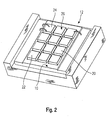
- FIG. 2 Another embodiment of a dental restoration device according to the invention can be seen from Fig. 2.
- the chips 12 are mounted closely adjacent and here too is one first group 22 from the semiconductor radiation sources 24 and a second group 20 of semiconductor radiation sources 26 is provided.
- the Dental restoration device according to the invention With the control device according to the invention are first the semiconductor radiation sources 24 switched on, the Dental restoration device according to the invention in immediate Neighborhood with the surface of the restoration part to be hardened has been brought. In this state the first catalyst activates and leads to pre-curing the photopolymerizable mass.
- post-processing may be carried out, if this is considered necessary. Also, for example another layer of dental restoration material be applied.
- the semiconductor radiation sources become the second Group 20 turned on and there is a hardening performed.
- FIG 3 shows the emission of the dental restoration device according to the invention in the state when all semiconductor radiation sources are switched on. It is a first maximum 30 and a second maximum 32 can be seen, the light intensity the second maximum 32, which is around 420 nm, is significantly higher.
Landscapes
- Health & Medical Sciences (AREA)
- Oral & Maxillofacial Surgery (AREA)
- Dentistry (AREA)
- Epidemiology (AREA)
- Life Sciences & Earth Sciences (AREA)
- Animal Behavior & Ethology (AREA)
- General Health & Medical Sciences (AREA)
- Public Health (AREA)
- Veterinary Medicine (AREA)
- Dental Tools And Instruments Or Auxiliary Dental Instruments (AREA)
Applications Claiming Priority (2)
| Application Number | Priority Date | Filing Date | Title |
|---|---|---|---|
| DE10125340 | 2001-05-23 | ||
| DE10125340A DE10125340B4 (de) | 2001-05-23 | 2001-05-23 | Dentales Lichtgerät |
Publications (2)
| Publication Number | Publication Date |
|---|---|
| EP1260193A2 true EP1260193A2 (fr) | 2002-11-27 |
| EP1260193A3 EP1260193A3 (fr) | 2003-05-21 |
Family
ID=7685992
Family Applications (1)
| Application Number | Title | Priority Date | Filing Date |
|---|---|---|---|
| EP02008013A Withdrawn EP1260193A3 (fr) | 2001-05-23 | 2002-04-10 | Dispositif d'éclairage dentaire |
Country Status (4)
| Country | Link |
|---|---|
| EP (1) | EP1260193A3 (fr) |
| JP (1) | JP3629475B2 (fr) |
| CA (1) | CA2383181A1 (fr) |
| DE (1) | DE10125340B4 (fr) |
Cited By (4)
| Publication number | Priority date | Publication date | Assignee | Title |
|---|---|---|---|---|
| DE102007011637A1 (de) * | 2007-03-09 | 2008-09-18 | Ivoclar Vivadent Ag | Lichtemissionsvorrichtung |
| US8113831B2 (en) | 2006-07-31 | 2012-02-14 | Ivoclar Vivadent Ag | Hand-held light curing device |
| EP2465466A1 (fr) * | 2010-12-20 | 2012-06-20 | Ivoclar Vivadent AG | Appareil dentaire manuel |
| WO2024051274A1 (fr) * | 2022-09-09 | 2024-03-14 | 桂林市啄木鸟医疗器械有限公司 | Module électroluminescent, source de lumière et machine de photopolymérisation dentaire |
Families Citing this family (5)
| Publication number | Priority date | Publication date | Assignee | Title |
|---|---|---|---|---|
| DE10155034B4 (de) * | 2001-11-09 | 2006-03-09 | Ivoclar Vivadent Ag | Lichthärtgerät und Verfahren zum Polymerisieren von polymerisierbaren Massen |
| DE102006015336B4 (de) | 2006-04-03 | 2015-05-07 | Ivoclar Vivadent Ag | Halbleiter-Strahlungsquelle, Lichthärtgerät mit Halbleiter-Strahlungsquelle, Beleuchtungsgerät mit Halbleiter-Strahlungsquelle und Verwendung eines Beleuchtungsgeräts mit Halbleiter-Strahlungsquelle |
| EP2489344B1 (fr) | 2011-02-15 | 2021-03-24 | Ivoclar Vivadent AG | Matériau dentaire comprenant une substance anti-microbienne |
| EP2801335B1 (fr) | 2013-05-07 | 2018-03-14 | Ivoclar Vivadent AG | Seringue |
| EP3013306B1 (fr) | 2013-06-27 | 2020-07-22 | Ivoclar Vivadent, Inc. | Oxyde de zirconium nanocristallin et ses procédés de fabrication |
Citations (1)
| Publication number | Priority date | Publication date | Assignee | Title |
|---|---|---|---|---|
| DE29511927U1 (de) | 1995-07-24 | 1997-01-09 | Thera Ges Fuer Patente | Lichtpolymerisationsgerät |
Family Cites Families (8)
| Publication number | Priority date | Publication date | Assignee | Title |
|---|---|---|---|---|
| DE3404904C2 (de) * | 1984-02-11 | 1986-01-16 | Kulzer & Co GmbH, 6393 Wehrheim | Verfahren zur Herstellung von kieferorthopädischen Geräten und Apparaturen |
| US5420768A (en) * | 1993-09-13 | 1995-05-30 | Kennedy; John | Portable led photocuring device |
| DE29511297U1 (de) * | 1995-07-12 | 1995-12-14 | Sanitaetshaus Korn | Bremsen-Nachrüstsatz für Räder |
| EP0780103A3 (fr) * | 1995-12-22 | 1997-12-03 | Heraeus Kulzer GmbH | Appareil d'irradiation |
| DE19721311C1 (de) * | 1997-05-21 | 1998-12-03 | Eka Ges Fuer Medizinisch Tech | Bestrahlungsgerät zur Polymerisation von lichthärtenden Kunststoffen |
| EP1031326A1 (fr) * | 1999-02-05 | 2000-08-30 | Jean-Michel Decaudin | Dispositif permettant la photo-activation de matériaux composites photosensibles utilisés notamment dans le domaine dentaire |
| EP1090607A1 (fr) * | 1999-10-08 | 2001-04-11 | Mectron S.R.L. | Pièce à main dentaire pour la polymérisation de composites ou résines photopolymérisables |
| IT1321003B1 (it) * | 2000-05-03 | 2003-12-18 | Mcm Srl | Metodo per il bloccaggio amovibile di solette a corrispondenti formemediante fascetta di nastro adesivo e dispositivo che attua tale |
-
2001
- 2001-05-23 DE DE10125340A patent/DE10125340B4/de not_active Expired - Fee Related
-
2002
- 2002-04-10 EP EP02008013A patent/EP1260193A3/fr not_active Withdrawn
- 2002-04-24 CA CA002383181A patent/CA2383181A1/fr not_active Abandoned
- 2002-05-23 JP JP2002149882A patent/JP3629475B2/ja not_active Expired - Fee Related
Patent Citations (1)
| Publication number | Priority date | Publication date | Assignee | Title |
|---|---|---|---|---|
| DE29511927U1 (de) | 1995-07-24 | 1997-01-09 | Thera Ges Fuer Patente | Lichtpolymerisationsgerät |
Cited By (5)
| Publication number | Priority date | Publication date | Assignee | Title |
|---|---|---|---|---|
| US8113831B2 (en) | 2006-07-31 | 2012-02-14 | Ivoclar Vivadent Ag | Hand-held light curing device |
| DE102007011637A1 (de) * | 2007-03-09 | 2008-09-18 | Ivoclar Vivadent Ag | Lichtemissionsvorrichtung |
| EP2465466A1 (fr) * | 2010-12-20 | 2012-06-20 | Ivoclar Vivadent AG | Appareil dentaire manuel |
| EP2465467A1 (fr) * | 2010-12-20 | 2012-06-20 | Ivoclar Vivadent AG | Appareil dentaire manuel |
| WO2024051274A1 (fr) * | 2022-09-09 | 2024-03-14 | 桂林市啄木鸟医疗器械有限公司 | Module électroluminescent, source de lumière et machine de photopolymérisation dentaire |
Also Published As
| Publication number | Publication date |
|---|---|
| JP2002360614A (ja) | 2002-12-17 |
| JP3629475B2 (ja) | 2005-03-16 |
| DE10125340B4 (de) | 2004-08-05 |
| EP1260193A3 (fr) | 2003-05-21 |
| CA2383181A1 (fr) | 2002-11-23 |
| DE10125340A1 (de) | 2002-12-05 |
Similar Documents
| Publication | Publication Date | Title |
|---|---|---|
| DE102006015336B4 (de) | Halbleiter-Strahlungsquelle, Lichthärtgerät mit Halbleiter-Strahlungsquelle, Beleuchtungsgerät mit Halbleiter-Strahlungsquelle und Verwendung eines Beleuchtungsgeräts mit Halbleiter-Strahlungsquelle | |
| DE102004063824B4 (de) | Leuchtdioden-Baugruppe mit antiparallelem Diodenchip | |
| DE10258193B4 (de) | Verfahren zum Herstellen von Leuchtdioden-Lichtquellen mit Lumineszenz-Konversionselement | |
| DE10125341B4 (de) | Bestrahlungsvorrichtung und Lichthärtgerät | |
| EP0879582A2 (fr) | Appareil à rayonnement pour la polymérisation de résines | |
| DE102005053218A1 (de) | LED-Vorrichtung und Verfahren zum Herstellung derselben | |
| EP1260193A2 (fr) | Dispositif d'éclairage dentaire | |
| EP3308740B1 (fr) | Appareil de durcissement à la lumière pour matériaux de restauration dentaire | |
| DE112018000656T5 (de) | LED-Baugruppe und Verfahren zur Herstellung derselben | |
| WO2011006754A1 (fr) | Diode luminescente et procédé de fabrication d'une diode luminescente | |
| DE10104579A1 (de) | Lichthärtgerät | |
| WO2014019795A1 (fr) | Procédé de fabrication d'un élément luminescent | |
| DE102013209735A1 (de) | Verfahren zum Herstellen eines patientenspezifischen Ersatzbrackets für eine kieferorthopädische Behandlung sowie nach dem Verfahren hergestelltes Bracket | |
| DE102014113844A1 (de) | Verfahren zum Herstellen eines optoelektronischen Bauelements und optoelektronisches Bauelement | |
| EP2396158B1 (fr) | Procédé et moule de fabrication d'un luminaire à diodes | |
| EP1046381B1 (fr) | Appareil de photopolymérisation | |
| DE10125343C2 (de) | Beleuchtungsvorrichtung | |
| DE102010031732A1 (de) | Optoelektronisches Bauelement | |
| EP3106123B1 (fr) | Dispositif dentaire de durcissement à la lumière | |
| DE102014205470B4 (de) | Leuchtvorrichtung mit CoB-Bereich | |
| DE102016125022A1 (de) | Herstellung von leuchtvorrichtungen | |
| DE10155034B4 (de) | Lichthärtgerät und Verfahren zum Polymerisieren von polymerisierbaren Massen | |
| CH676789A5 (fr) | ||
| WO2014086784A1 (fr) | Diode électroluminescente présentant plusieurs zones à substance fluorescente | |
| DE102010046790A1 (de) | Optoelektronisches Halbleiterbauelement und Verfahren zu dessen Herstellung |
Legal Events
| Date | Code | Title | Description |
|---|---|---|---|
| PUAI | Public reference made under article 153(3) epc to a published international application that has entered the european phase |
Free format text: ORIGINAL CODE: 0009012 |
|
| AK | Designated contracting states |
Kind code of ref document: A2 Designated state(s): AT BE CH CY DE DK ES FI FR GB GR IE IT LI LU MC NL PT SE TR |
|
| AX | Request for extension of the european patent |
Free format text: AL;LT;LV;MK;RO;SI |
|
| PUAL | Search report despatched |
Free format text: ORIGINAL CODE: 0009013 |
|
| AK | Designated contracting states |
Designated state(s): AT BE CH CY DE DK ES FI FR GB GR IE IT LI LU MC NL PT SE TR |
|
| AX | Request for extension of the european patent |
Extension state: AL LT LV MK RO SI |
|
| 17P | Request for examination filed |
Effective date: 20031024 |
|
| AKX | Designation fees paid |
Designated state(s): AT BE CH CY DE DK ES FI FR GB GR IE IT LI LU MC NL PT SE TR |
|
| 17Q | First examination report despatched |
Effective date: 20050214 |
|
| STAA | Information on the status of an ep patent application or granted ep patent |
Free format text: STATUS: THE APPLICATION HAS BEEN WITHDRAWN |
|
| 18W | Application withdrawn |
Effective date: 20180905 |
|
| RIC1 | Information provided on ipc code assigned before grant |
Ipc: A61C 19/00 20060101ALI20020902BHEP Ipc: A61C 13/15 20060101AFI20020902BHEP |