EP1257051A2 - FM-Demodulator mit Nachbarkanalunterdrückung - Google Patents
FM-Demodulator mit Nachbarkanalunterdrückung Download PDFInfo
- Publication number
- EP1257051A2 EP1257051A2 EP02100461A EP02100461A EP1257051A2 EP 1257051 A2 EP1257051 A2 EP 1257051A2 EP 02100461 A EP02100461 A EP 02100461A EP 02100461 A EP02100461 A EP 02100461A EP 1257051 A2 EP1257051 A2 EP 1257051A2
- Authority
- EP
- European Patent Office
- Prior art keywords
- signal
- circuit
- demodulator
- input signal
- phase
- Prior art date
- Legal status (The legal status is an assumption and is not a legal conclusion. Google has not performed a legal analysis and makes no representation as to the accuracy of the status listed.)
- Granted
Links
Images


Classifications
-
- H—ELECTRICITY
- H03—ELECTRONIC CIRCUITRY
- H03D—DEMODULATION OR TRANSFERENCE OF MODULATION FROM ONE CARRIER TO ANOTHER
- H03D3/00—Demodulation of angle-, frequency- or phase- modulated oscillations
- H03D3/02—Demodulation of angle-, frequency- or phase- modulated oscillations by detecting phase difference between two signals obtained from input signal
- H03D3/06—Demodulation of angle-, frequency- or phase- modulated oscillations by detecting phase difference between two signals obtained from input signal by combining signals additively or in product demodulators
Definitions
- the invention relates to an anti-demodulator circuit, a filter device and Demodulator circuit.
- An anti-demodulator circuit in the sense of this invention works basically similarly like a demodulator circuit, but suppresses the desired useful signal and improves the noise-signal ratio.
- the anti-demodulator circuit can basically be constructed like a known demodulator circuit, but used instead of one Bandpass filter a notch filter (NOTCH filter) as a phase shifter or delay element.
- NOTCH filter notch filter
- US-A-5 307 517 describes an adaptive notch filter for the suppression of FM interference in FM receiving stations.
- Figure 5 of this document shows a circuit arrangement with two PLL demodulators and two upstream notch filters, the notch filters in this arrangement cannot be used for phase shifting.
- One branch of the Demodulator circuit is used to demodulate a strong signal and the other for Demodulation of a weak signal.
- the input signal comprises both useful signals, i.e. the strong and the weak signal, and other, smaller interference signals.
- the demodulator of the The first branch is set to the stronger signal (locked) and sets the notch filter of the second branch to the same resonance frequency on
- the demodulator of the second Zweig is set to the smaller signal (locked) and sets the notch filter of the first Branch to the same resonance frequency.
- the notch filters are not part of the actual demodulator, but upstream of it.
- the notch filters are also not based on the respective useful signals of the branch in which they are provided to be matched, but they are set to match each branch suppress the unwanted signal, as is common in the prior art.
- JP 0590040308AA, JP 0060069821AA and JP 0030004630AA each describe the Use of Kexbfilter in connection with demodulators to improve the signal-to-noise ratio.
- DE-A-3840999 describes a circuit arrangement for suppression narrowband interference signals in a receiver, with a tuning system in the Receiver sets a desired frequency band.
- An arithmetic unit calculates the difference between the frequency the receiver is tuned to and the frequency of the greatest disruptor and controls a PLL oscillator depending on it. The frequency will be like this set so that the interferer falls within the range of a notch filter.
- the output signal of the Kexbfilter is thus freed from the interference and forms an input signal of the Demodulator.
- IF filters are used with unchangeable filter characteristics, e.g. Ceramic filter, used outside the integrated circuits of the radio receiver must be implemented as external components, and therefore represent a significant cost factor.
- Adjacent channel suppression when receiving a transmitter must have several such filters in Series are switched.
- Philips Corp. are radio receivers for radios, and especially for high quality car radios, described, in which at least a part of the implemented by the IF filters in the IF path Selection is realized in an integrated circuit.
- integrated filters can depending on the signal conditions of the received FM signals in their bandwidth to be changed.
- the bandwidth of the filters are designed to be large while occurring the bandwidth of interference signals should be reduced accordingly.
- the Integrated filter controlled by an adjacent channel detector (ACD) depending on the interferer whose input signal is the output signal of the FM demodulator (MPX signal).
- ACD adjacent channel detector
- MPX signal the FM demodulator
- the FM demodulator is set to the IF input signal and to the IF useful signal optimized. If one or more interference signals occur, this FM demodulator delivers thus to the adjacent channel detector a signal with a relatively high useful signal-to-noise ratio and thus a relatively poor signal-to-noise ratio.
- Figures 1 and 2 show the basic structure of those known from the prior art FM demodulators.
- FIG. 3 shows a circuit diagram of a more advanced demodulator according to U.S. patent 5,341,107 to which reference is made.
- Phase shifters implemented as a first-order bandpass filter or resonance amplifier 10, whose resonance frequency can be controlled linearly.
- the bandpass filter is set to 0 ° (INCOS) and - 90 ° (INSIN) input signals driven.
- the circuit has a cosine path and a sine path, the transfer function being identical for both paths and the Phase difference between the two paths for all frequencies is 90 °.
- the phase response of each path essentially corresponds to that of a first-order bandpass.
- the demodulator shown in FIG. 3 forms a via a resonance frequency control input 12 of the band pass 10 closed loop.
- the center frequency f0 of the Bandpass 10 is through the feedback of the output signal OMPX, the demodulated input signal always corresponds to the instantaneous frequency of the FM input signals set. At this frequency the phase shift is in one path equals zero. Thus, the input signals of the mixers 14, 16 of the two paths are 90 ° out of phase, and when stable, the output signals are virtually zero.
- the demodulated output signal OMPX is used directly in the closed loop become.
- the demodulated output signal OMPX is shown in FIG Demodulator circuit by adding or subtracting the output signals of the Cosine path and the sinus path formed, one provided for this Adder circuit 18 also a loop filter (LOOP filter) 20 and one Amplifier circuit 22 are connected downstream
- the frequency of the output signal corresponds to the amount of f0-f1.
- radio receiver applications can be for a jammer of an adjacent channel for example a frequency of 100 kHz or 200 kHz above or below the Frequency of the useful signal can be assumed. So that is the frequency of the output signal OMPX is the difference frequency of 100 kHz or 200 kHz.
- the amplitude of the Output signal depends on the amplitude distance of the input signals and on Frequency spacing.
- the frequency dependence results from the quality of the bandpass 10, which in turn determines the bandwidth of the demodulator in FIGS. 1 and 2.
- the Demodulator bandwidth should be at least as large as the maximum frequency spacing.
- the bandwidth of the demodulator over the cutoff frequency of the loop filter 20 can be set. In practice, this only occurs with a small amplitude distance a disturbance signal and useful signal a direct current signal or direct current offset.
- the demodulator bandwidth is influenced by the quality of the bandpass 10, but mainly determined by the cutoff frequency of the loop filter 20.
- the demodulator circuits shown in Figures 1 to 3 for a Adjacent channel detection can be used, for example, in a radio receiver Filter device for a specific adjacent channel suppression depending on the interferer adjust, these circuit arrangements have the disadvantage that the demodulated signal OMPX has a bad interference-to-use ratio (desired per se) because of the bandpass 10 dampens the interferer in relation to the useful signal.
- the demodulator requires a much higher bandwidth than usual. This in turn leads to a reduction in the performance for the demodulation of the useful signal.
- the Output of the demodulator circuit shown in Figure 3 would e.g. the shares higher harmonic vibrations of frequency f0 increase in the Mixer circuits 14, 16 arise.
- the quality of the band pass 10 can at Increasing the bandwidth can no longer be optimally matched to the useful signal. Measurements have further shown that with a reduction in the bandwidth of the Bandpass filter 10 the behavior with respect to interference signals which occur when two or more signals can arise at the antenna input in the further signal path (so-called whistle behavior) is significantly improved.
- a useful signal and a modulated interference signal are those in the demodulated signal OMPX contained portions of the useful signal (as desired) very large and would have to Considerable effort to filter this signal for the adjacent channel suppression to be able to use.
- the relatively weak signal on the other hand, caused by the interferer f0-f1 is generated, must be prepared with a correspondingly large amount of circuitry to set the filter device for the adjacent channel suppression.
- the Frequency dependence of the difference frequency between useful signal and interference signal further deteriorates the function for controlling the IF filter device.
- the interference signal and the useful signal only appear when the amplitude distance is small a DC offset that occurs abruptly at a certain point.
- This can be detected by an offset detector, processed and used to control the Filter device can be used additively.
- the offset detector must have a high gain and thus a correspondingly high one
- Have circuit complexity, in addition a relatively complex adjustment in practice in relation to direct current offset, which have a different origin, that is DC offset that occurs at the demodulator output and not through the interferer are caused.
- the abrupt occurrence at a certain, small amplitude spacing of the DC offset also requires a very fast-reacting system, which in in practice sensitive to scattering of the stability and immunity to interference integrated components.
- the invention is therefore based on the object of a demodulator circuit for FM radio receiver devices high quality, effective and simple Supports adjacent channel suppression and minimal circuitry requires.
- the anti-demodulator circuit according to the invention is basically like one Demodulator circuit constructed, but has a notch filter instead of the bandpass filter, which receives an input signal comprising a useful signal and an interference signal, and a Filtered signal generated, the notch filter has a center frequency which is approximately that Frequency of the input signal corresponds to at least part of the useful signal suppress.
- the anti-demodulator circuit further includes a mixer circuit that receives the filtered signal and a phase-shifted input signal and on outputs demodulated output signal that largely corresponds to the interference signal.
- the basic concept of this invention is thus based on an anti-demodulator circuit which a notch filter or notch filter instead of that in the demodulators of the prior art usual bandpass filter and suppresses the desired signal (useful signal) and the noise-signal ratio improved.
- a phase shifter network is in series with the notch filter switched to a low current offset with a high signal-to-noise ratio to obtain.
- the notch filter can be obtained by subtracting the Output signal of a bandpass filter can be realized from its input signal. This is particularly favorable if a conventional demodulator and an anti-demodulator according to the Invention can be used in combination to generate a demodulated interference signal for the Adjacent channel suppression and a demodulated useful signal for the radio receiver obtained, the bandpass filter being used in both demodulators can, thereby avoiding redundant components.
- the notch filter is a Pulse shaping stage downstream to higher harmonic vibrations up to a to suppress some degree.
- the invention also provides a filter device for suppressing interference signals and in particular from adjacent channel interference that an anti-demodulator circuit of the above described type, the bandwidth of the filter device depending on the Output signal of the anti-demodulator circuit is controlled.
- the invention also provides a demodulator circuit with a Bandpass filter circuit and an anti-demodulator circuit of the type described above in Combination and especially in parallel.
- the anti-demodulator circuit according to the invention can be integrated, for example Circuit for FM radio receivers are used, which fully integrated IF filter device with tunable bandwidth.
- the bandwidth can depend on the size of the disturbance in the signal field can be continuously adjusted, starting from a wide band if there is no interference up to a very narrow band for big disturbances.
- the control signal for controlling the bandwidth is from the output of the anti-demodulator according to the invention in parallel via an adjacent channel detector (ACD) and detects an offset detector. Because the anti-demodulator optimizes for the interference signal the signal-to-noise ratio or the signal-to-noise ratio becomes high.
- the anti-demodulator circuit With the anti-demodulator circuit according to the invention, a large part of the Circuit complexity and thus valuable chip area for filtering and amplifying the Output signal of the demodulator for the adjacent channel suppression, because with the anti-demodulator the interference signal can already be optimally detected.
- the system is less susceptible to scattering of internal components, stability and reliability are significantly increased compared to the prior art.
- FIGs 1 to 3 show circuit diagrams of demodulator circuits that Bandpass filter use, according to the prior art, Figure 3 on an earlier Patent application by the same applicant.
- FIG. 1 a first-order bandpass filter circuit is designated 10
- a 90 ° phase shifter circuit is indicated at 24
- a mixer circuit is at 26 designated.
- Corresponding components are identified in FIG. 2 with the same reference symbols.
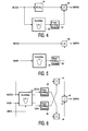
- FIGS. 1 to 3 show a first, a second and a third embodiment of the Anti-demodulator according to the invention, wherein the circuits Demodulator circuits of FIGS. 1 to 3 correspond to the bandpass filter circuit 10 however, was replaced by a notch filter circuit, or NOTCH filter 30.
- the anti-demodulator circuit of FIG. 4 includes a micro filter circuit 30 Phase shifter network 32, a fixed 90 ° phase shifter 34 and one Mixer circuit 36 which are interconnected in the manner shown in Figure 4.
- the anti-demodulator circuit of FIG. 4 also receives a 0 ° signal as an input signal an interference signal component and a useful signal component and generates an at its output demodulated interference signal OMPXA with a high interference-to-use ratio because of the notch filter 30 can suppress a large part of the useful signal.
- the alternative circuit structure of FIG. 5 includes a notch filter circuit 30 Phase shifter network 32 and a mixer circuit 38 which is based on that shown in FIG Are wise with each other
- the anti-demodulator circuit of FIG. 5 basically works like the circuit of FIG Figure 4, wherein the anti-demodulator circuit as input signals a 0 ° signal and a Receives 90 ° signal, so that the 90 ° phase shifter of the circuit of Figure 4 is omitted can be.
- the 0 ° signal and the 90 ° signal can also be exchanged become
- Adjacent channel detector which the output signal OMPXA of the anti-demodulator as Control signal used, and be significantly reduced in the offset detector, being in the adjacent channel detector in particular, simpler filters and a lower gain can be used and in the offset detector less gain and none Offset adjustment are necessary.
- FIG. 6 shows a further embodiment of the anti-demodulator according to the invention a notch filter circuit 30, two phase shifter networks 40, 42, two Mixer circuits 44, 46 and an adder stage 48, in the manner shown in Figure 6 are interconnected.
- the anti-demodulator of Figure 6 comprises, according to the Demodulator of Figure 3, a cosine branch and a sine branch, with the 6 the useful signal can be virtually completely suppressed, because the center frequency of the notch filter circuit 30 via a control input 50 using of the demodulated useful signal OMPX always to the instantaneous frequency of the Input signal can be set.
- the anti-demodulator of Figure 6 operates similarly to the demodulator circuit of the figure 3, wherein the output signal OMPXA corresponds to the demodulated interference signal that receives practically no part of the useful signal. If such an anti-demodulator circuit used in an FM radio receiver for adjacent channel detection the bandwidth of the demodulator of the radio receiver can be optimally adjusted to that User signal can be matched.
- FIG. 7 shows: a circuit for implementing the notch filter circuit of the anti-demodulator according to the invention with the aid of a bandpass filter, which has the particular advantage that the notch filter can be implemented using the demodulator bandpass, which is regularly present in an FM radio receiver, for example. This considerably reduces the circuitry for the anti-demodulator according to the invention.
- the notch filter circuit of Figure 7, incorporating the demodulator bandpass filter, includes one Bandpass filter 52, a pulse shaping stage 54 and an adder stage 56, which refer to the in Figure 7 are shown interconnected.
- the input signal of the notch filter is on 0 ° input signal INCOS, and the output signal is as a notch filter output signal Referred to ONOTCH.
- the input signal INCOS or INSIN of the Kerib filter circuit is on Square-wave signal, in particular an output signal of an upstream limiter.
- the bandpass filter 52 in series-connected pulse shaping stage 54 Suppression of the useful signal, e.g. regarding higher harmonic vibrations, be optimized.
- the pulse shaping stage 54 is not a negative feedback differential amplifier realized.
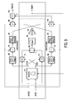
- Figures 8 and 9 show two preferred embodiments of the invention Anti-demodulator in combination with a conventional demodulator minimal circuitry are realized.
- the embodiment of Figure 8 corresponds the representation of Figure 2
- the embodiment of Figure 9 corresponds to the representation of Figure 3, wherein in Figure 9, the demodulator part by a dashed rectangle is limited.
- the anti-demodulator / demodulator circuit of Figure 8 includes one Bandpass filter circuit 60, a pulse shaping stage 62, a mixer circuit 64, a Adder stage 66, a phase shifter network 68 and a further mixer circuit 70, connected in the manner shown in Figure 8.
- the anti-demodulator / demodulator circuit combines the demodulator function of FIG. 2 and the anti-demodulator function 5, wherein the notch filter circuit 30 of FIG circuit shown in Figure 7 is replaced.
- FIG. 9 shows a preferred embodiment of an anti-demodulator / demodulator circuit according to the invention.
- This comprises a bandpass filter circuit 72, two Mixer circuits 74 and 78, an adder 80, a loop filter circuit 82, one Amplifier stage 84, two pulse shaping stages 86, 88, two further adder stages 90, 92, two phase shifter networks 94, 96, two further mixer circuits 98, 100 and one further adder stage 102, which are connected to one another in the manner shown in FIG
- the anti-demodulator / demodulator circuit of FIG. 9 comprises a demodulator, which corresponds to the embodiment of Figure 3 and by the dashed box is identified.
Landscapes
- Engineering & Computer Science (AREA)
- Power Engineering (AREA)
- Noise Elimination (AREA)
- Stereo-Broadcasting Methods (AREA)
- Circuits Of Receivers In General (AREA)
Abstract
Description
- Bandpaß
- 10
- Resonanzfrequenz-Steuereingang
- 12
- Mischer
- 14, 16
- Addiererschaltkreis
- 18
- Loop-Filter
- 20
- Verstärkerschaltung
- 22
- Phasenschieberschaltung
- 24
- Mischerschaltkreis
- 26
- Kerbfilterschaltkreis
- 30
- Phasenschiebernetzwerk
- 32, 34
- Mischerschaltkreis
- 36, 38
- Phasenschiebernetzwerk
- 40, 42
- Mischerschaltkreis
- 44, 46
- Addiererstufe
- 48
- Steuereingang
- 50
- Bandpaßfilter
- 52
- Pulsformungsstufe
- 54
- Addiererstufe
- 56
- Bandpaßfilterschaltkreis
- 60
- Pulsformungsstufe
- 62
- Mischerschaltkreis
- 64
- Addiererstufe
- 66
- Phasenschiebernetzwerk
- 68
- Mischerschaltkreis
- 70
- Bandpaßfilteischaltkreis
- 72
- Mischerschaltkreis
- 74, 78
- Addiererstufe
- 80
- Loopfilterschaltung
- 82
- Verstärkerstufe
- 84
- Pulsformungsstufe
- 86, 88
- Addiererstufe
- 90, 92
- Phasenschiebernetzwerk
- 94, 96
- Mischerschaltkreis
- 98, 100
- Addiererstufe
- 102
Claims (15)
einem Mischerschaltkreis (36; 38), der das gefilterte Signal und ein phasenverschobenes Eingangssignal (INSIN) empfängt und ein demoduliertes Ausgangsignal (OMPXA) ausgibt, das dem Störsignal weitgehend entspricht.
dadurch gekennzeichnet, dass ein Phasenschiebernetzwerk (32) in Reihe mit dem Kerbfilter (30) geschaltet ist.
gekennzeichnet durch einen dem Mischerschaltkreis (36; 38) vorgeschalteten 90°-
Phasenschieber zur Erzeugung eines um 90° phasenverschobenen Eingangssignals (INSIN) für den Mischelschaltkreis (36; 38).
dadurch gekennzeichnet, dass das Kerbfilter (30) das Eingangssignal (INCOS) und ein um 90°
phasenverschobenes Eingangssignal (INSIN) empfängt und zwei um 90° phasenverschobene Kerbfilter-Ausgangssignale (OCOS, OSIN) erzeugt,
dem Kerbfilter (30) ein Phasenschiebernetzwerk (40, 42) nachgeschaltet ist, welches die Kerbfilter-Ausgangssignale (OCOS, OSIN) empfängt, und durch zwei
Demodulatorzweige, die jeweils einen Mischerschaltkreis (44, 46) aufweisen, wobei
ein erster Eingang eines ersten Mischerschaltkreises (44) das Eingangssignal empfängt und
ein zweiter Eingang des ersten Mischerschaltkreises (44) ein Ausgangsägnal des
Phasenschiebernetzwerkes empfängt, das auf dem um 90° phasenverschobenen Eingangssignal beruht, ein erster Eingang des zweiten Mischerschaltkreises (46) das um
90° phasenverschobene Eingangssignal empfängt und ein zweiter Eingang des zweiten Mischerschaltkreises (46) ein Ausgangssignal des Phasenschiebernetzwerkes empfängt, das auf dem nicht-phasenverschobenen Eingangssignal beruht, und wobei
die Ausgangssignale der Mischerschaltungen (44, 46) in einer Addiererschaltung (48) kombiniert werden, um ein demoduliertes Störsignal (OMPXA) zu erzeugen.
dadurch gekennzeichnet, dass die Mittenfrequenz des Kexbfilters (30) abhängig von dem Nutzsignal steuerbar ist.
dadurch gekennzeichnet, dass das Kerbfilter mithilfe eines Bandpaßfilters (52) gemäß der Formel "1 - A(BP) = A(Notch)" realisiert ist, wobei A(BP) die Übertragungsfunktion des Bandpaßfilters (52) und A(Notch) die Übertragungsfunktion des Kerbfilters ist.
dadurch gekennzeichnet, dass das Kerbfilter eine Bandpaßfilterschaltung (52; 60) und einen Addiererschaltkreis (56; 66) aufweist, die Bandpaßfilterschaltung (52; 60) das Eingangssignal empfängt und ein bandpaßgsfiltertes Eingangssignal erzeugt und der Addiererschaltkreis (56; 66) ein Kerbfilter-Ausgangssignal (ONOTCH) als eine Differenz des bandpaßgefilterten Eingangssignals und des Eingangssignals erzeugt.
dadurch gekennzeichnet, dass eine Pulsformungsstufe (54; 62) mit dem Kerbfilter in Reihe geschaltet ist.
gekennzeichnet durch eine Anti-Demodulatorschaltung nach einem der vorangehenden Ansprüche, wobei die Bandbreite der Filtereinrichtung abhängig von dem Ausgangssignal (OMPXA) der Anti-Demodulatorschaltung steuerbar ist.
dadurch gekennzeichnet, dass die Mittenfrequenz der Bandpaßfilterschaltung abhängig von dem demodulierten Nutzsignal (OMPX) steuerbar ist.
dadurch gekennzeichnet, dass das Bandpaßfilter (72) das Eingangssignal und das um 90° phasenverschobene Eingangssignal empfängt und dem Bandpaßfilter (72) zwei parallele Anti-Demodulatorzweige nachgsschaltet sind, welche jeweils einen Addiererschaltkreis (90, 92) aufweisen, um ein erstes und ein zweites, um 90° phasenverschobenes Kerbfilter-Ausgangssignals (ONOTCH COS, ONOTCH SEN) zu erzeugen, sowie zwei parallele Demodulatorzweige, welche jeweils einen Mischerschaltkreis (74, 78) aufweisen, um ein erstes und ein zweites, um 90° phasenverschobenes demoduliertes Nutzsignal zu erzeugen.
dadurch gekennzeichnet, dass die zwei Demodulatorzweige in einem Addiererschaltkreis (80) zusammengeführt sind, um eine Differenz aus dem demodulierten Nutzsignal und dem phasenverschobenen demodulierten Nutzsignal zu erzeugen, wobei dem Addiererschaltkreis (80) ein Verstärkerschaltkreis (84) nachgeschaltet ist.
dadurch gekennzeichnet, dass die Ausgänge der zwei Anti-Demodulatorzweige auf einen Addiererschaltkreis (102) geführt sind, um eine Differenz zwischen dem demodulierten Störsignal und dem phasenverschobenen demodulierten Störsignal zu bilden.
Applications Claiming Priority (2)
| Application Number | Priority Date | Filing Date | Title |
|---|---|---|---|
| DE10122748 | 2001-05-10 | ||
| DE10122748A DE10122748A1 (de) | 2001-05-10 | 2001-05-10 | Anti-Demodulatorschaltung, Filtereinrichtung und Demodulatorschaltung |
Publications (3)
| Publication Number | Publication Date |
|---|---|
| EP1257051A2 true EP1257051A2 (de) | 2002-11-13 |
| EP1257051A3 EP1257051A3 (de) | 2004-10-20 |
| EP1257051B1 EP1257051B1 (de) | 2007-11-14 |
Family
ID=7684300
Family Applications (1)
| Application Number | Title | Priority Date | Filing Date |
|---|---|---|---|
| EP02100461A Expired - Lifetime EP1257051B1 (de) | 2001-05-10 | 2002-05-08 | FM-Demodulator mit Nachbarkanalunterdrückung |
Country Status (5)
| Country | Link |
|---|---|
| US (1) | US6937871B2 (de) |
| EP (1) | EP1257051B1 (de) |
| JP (1) | JP4108365B2 (de) |
| AT (1) | ATE378727T1 (de) |
| DE (2) | DE10122748A1 (de) |
Cited By (2)
| Publication number | Priority date | Publication date | Assignee | Title |
|---|---|---|---|---|
| US8841964B2 (en) | 2010-03-10 | 2014-09-23 | Zurich Instruments Ag | Apparatus and method for demodulating an input signal |
| US20230140050A1 (en) * | 2021-10-28 | 2023-05-04 | University Corporation For Atmospheric Research | Band filter for filtering a discrete time series signal |
Families Citing this family (8)
| Publication number | Priority date | Publication date | Assignee | Title |
|---|---|---|---|---|
| JP4133604B2 (ja) * | 2003-06-10 | 2008-08-13 | アルパイン株式会社 | ラジオ受信機 |
| FR2876517B1 (fr) * | 2004-10-08 | 2009-04-10 | Groupe Ecoles Telecomm | Demodulateur et modulateur-demodulateur par conversion directe de frequence |
| EP1895662A4 (de) * | 2005-06-21 | 2010-08-04 | Pioneer Corp | Phasenkorrekturschaltung |
| GB0601198D0 (en) * | 2006-01-20 | 2006-03-01 | Cambridge Silicon Radio Ltd | FM Tone rejection |
| US8169551B2 (en) * | 2007-12-07 | 2012-05-01 | Himax Technologies Limited | Method and apparatus for adjusting center frequency of filter |
| US20090243850A1 (en) * | 2008-04-01 | 2009-10-01 | Yoshiteru Nishizato | Microwave receiver and microwave sensor system |
| US8116713B2 (en) * | 2008-11-26 | 2012-02-14 | Visteon Global Technologies, Inc. | Automatic bandwidth control with high-deviation detection |
| US10056662B2 (en) * | 2015-09-23 | 2018-08-21 | The United States Of America, As Represented By The Secretary Of The Navy | Switched bandstop filter with low-loss linear-phase bypass state |
Family Cites Families (9)
| Publication number | Priority date | Publication date | Assignee | Title |
|---|---|---|---|---|
| US3911366A (en) * | 1958-11-13 | 1975-10-07 | Elie J Baghdady | Receiver interference suppression techniques and apparatus |
| US4866779A (en) * | 1988-07-13 | 1989-09-12 | Delco Electronics Corporation | Adaptive AM audio processor |
| US5307517A (en) * | 1991-10-17 | 1994-04-26 | Rich David A | Adaptive notch filter for FM interference cancellation |
| TW214027B (en) * | 1992-06-12 | 1993-10-01 | Philips Electronics Nv | FM quadrature demodulator |
| US5357574A (en) * | 1992-12-14 | 1994-10-18 | Ford Motor Company | Coherent signal generation in digital radio receiver |
| CA2125468C (en) * | 1993-06-28 | 1998-04-21 | Danny Thomas Pinckley | Method of selectively reducing spectral components in a wideband radio frequency signal |
| US5613234A (en) * | 1994-10-28 | 1997-03-18 | Lucent Technologies Inc. | Receive filter using frequency translation for or in cellular telephony base station |
| US6807405B1 (en) * | 1999-04-28 | 2004-10-19 | Isco International, Inc. | Method and a device for maintaining the performance quality of a code-division multiple access system in the presence of narrow band interference |
| US6714776B1 (en) * | 1999-09-28 | 2004-03-30 | Microtune (Texas), L.P. | System and method for an image rejecting single conversion tuner with phase error correction |
-
2001
- 2001-05-10 DE DE10122748A patent/DE10122748A1/de not_active Withdrawn
-
2002
- 2002-05-07 US US10/140,500 patent/US6937871B2/en not_active Expired - Lifetime
- 2002-05-08 EP EP02100461A patent/EP1257051B1/de not_active Expired - Lifetime
- 2002-05-08 AT AT02100461T patent/ATE378727T1/de not_active IP Right Cessation
- 2002-05-08 DE DE50211182T patent/DE50211182D1/de not_active Expired - Lifetime
- 2002-05-10 JP JP2002135843A patent/JP4108365B2/ja not_active Expired - Fee Related
Cited By (3)
| Publication number | Priority date | Publication date | Assignee | Title |
|---|---|---|---|---|
| US8841964B2 (en) | 2010-03-10 | 2014-09-23 | Zurich Instruments Ag | Apparatus and method for demodulating an input signal |
| US20230140050A1 (en) * | 2021-10-28 | 2023-05-04 | University Corporation For Atmospheric Research | Band filter for filtering a discrete time series signal |
| US11888660B2 (en) * | 2021-10-28 | 2024-01-30 | University Corporation For Atmospheric Research | Band filter for filtering a discrete time series signal |
Also Published As
| Publication number | Publication date |
|---|---|
| DE50211182D1 (de) | 2007-12-27 |
| US6937871B2 (en) | 2005-08-30 |
| JP2003018031A (ja) | 2003-01-17 |
| ATE378727T1 (de) | 2007-11-15 |
| JP4108365B2 (ja) | 2008-06-25 |
| DE10122748A1 (de) | 2002-11-14 |
| US20020196878A1 (en) | 2002-12-26 |
| EP1257051B1 (de) | 2007-11-14 |
| EP1257051A3 (de) | 2004-10-20 |
Similar Documents
| Publication | Publication Date | Title |
|---|---|---|
| DE2211347C3 (de) | Schaltungsanordnung zur Veränderung des dynamischen Bereiches von Signalen | |
| DE2902952C2 (de) | Direktmischendes Empfangssystem | |
| DE2706364C3 (de) | Schaltungsanordnung zur Unterdrückung von impulsartigen Störungen in einem FM-Stereo-Rundfunkempfänger | |
| DE69313520T2 (de) | FM-Quadratur-Demodulator | |
| CH662914A5 (de) | Datenempfaenger fuer ein fm-eingangssignal. | |
| DE2142660A1 (de) | Abstimm- und Empfangsfeldstärke-Anzeigeschaltung | |
| DE69833345T2 (de) | Vorrichtung und Verfahren zum Steuern der Frequenzcharakteristik eines Filters | |
| EP1257051B1 (de) | FM-Demodulator mit Nachbarkanalunterdrückung | |
| WO2012031684A1 (de) | Schaltungsanordnung zur erzeugung von eine breitbandige frequenzrampe bildenden hochfrequenten ausgangssignalen | |
| DE3210454A1 (de) | Empfaenger-eingangsschaltung | |
| EP0617519A2 (de) | Schaltungsanordnung zur Ableitung mindestens eines von der Qualität eines empfangenen Signals abhängigen Qualitätssignals | |
| DE69623412T2 (de) | Gerät zum korrigieren der amplituden-/frequenzcharakteristik eines ein kabel durchlaufenden signals und entsprechender frequenzentzerrer | |
| DE3131892C2 (de) | Frequenztrennvorrichtung | |
| DE2754250B2 (de) | AM/FM-Frequenzdiskriminator | |
| EP1875607B1 (de) | Eingangsfilter zur spiegelfrequenzunterdrückung | |
| DE3412191C2 (de) | ||
| WO1995003650A1 (de) | Zf-filteranordnung für fm-empfangssignale | |
| EP0133730B1 (de) | Empfängerschaltung | |
| EP0185414B1 (de) | FM-Stereoempfänger | |
| DE2730153A1 (de) | Verfahren und vorrichtung zum empfangen von radiosignalen nach dem ueberlagerungsprinzip | |
| DE1277944B (de) | Frequenzumsetzer | |
| DE102008031643A1 (de) | Empfängeranordnung, insbesondere zum Einsatz in Kraftfahrzeugen | |
| DE1285020B (de) | Verfahren und Einrichtung zur kompatiblen Einseitenbanduebertragung | |
| WO2008037539A1 (de) | Funkempfänger | |
| DE2833053A1 (de) | Kanalwaehler fuer einen fernsehempfaenger |
Legal Events
| Date | Code | Title | Description |
|---|---|---|---|
| PUAI | Public reference made under article 153(3) epc to a published international application that has entered the european phase |
Free format text: ORIGINAL CODE: 0009012 |
|
| AK | Designated contracting states |
Kind code of ref document: A2 Designated state(s): AT BE CH CY DE DK ES FI FR GB GR IE IT LI LU MC NL PT SE TR |
|
| AX | Request for extension of the european patent |
Free format text: AL;LT;LV;MK;RO;SI |
|
| RAP1 | Party data changed (applicant data changed or rights of an application transferred) |
Owner name: KONINKLIJKE PHILIPS ELECTRONICS N.V. Owner name: PHILIPS INTELLECTUAL PROPERTY & STANDARDS GMBH |
|
| PUAL | Search report despatched |
Free format text: ORIGINAL CODE: 0009013 |
|
| AK | Designated contracting states |
Kind code of ref document: A3 Designated state(s): AT BE CH CY DE DK ES FI FR GB GR IE IT LI LU MC NL PT SE TR |
|
| AX | Request for extension of the european patent |
Extension state: AL LT LV MK RO SI |
|
| 17P | Request for examination filed |
Effective date: 20050420 |
|
| AKX | Designation fees paid |
Designated state(s): AT BE CH CY DE DK ES FI FR GB GR IE IT LI LU MC NL PT SE TR |
|
| 17Q | First examination report despatched |
Effective date: 20051219 |
|
| GRAP | Despatch of communication of intention to grant a patent |
Free format text: ORIGINAL CODE: EPIDOSNIGR1 |
|
| RAP1 | Party data changed (applicant data changed or rights of an application transferred) |
Owner name: NXP B.V. |
|
| GRAS | Grant fee paid |
Free format text: ORIGINAL CODE: EPIDOSNIGR3 |
|
| GRAA | (expected) grant |
Free format text: ORIGINAL CODE: 0009210 |
|
| AK | Designated contracting states |
Kind code of ref document: B1 Designated state(s): AT BE CH CY DE DK ES FI FR GB GR IE IT LI LU MC NL PT SE TR |
|
| REG | Reference to a national code |
Ref country code: GB Ref legal event code: FG4D Free format text: NOT ENGLISH |
|
| REG | Reference to a national code |
Ref country code: CH Ref legal event code: EP |
|
| REG | Reference to a national code |
Ref country code: IE Ref legal event code: FG4D Free format text: LANGUAGE OF EP DOCUMENT: GERMAN |
|
| REF | Corresponds to: |
Ref document number: 50211182 Country of ref document: DE Date of ref document: 20071227 Kind code of ref document: P |
|
| GBT | Gb: translation of ep patent filed (gb section 77(6)(a)/1977) |
Effective date: 20071206 |
|
| PG25 | Lapsed in a contracting state [announced via postgrant information from national office to epo] |
Ref country code: NL Free format text: LAPSE BECAUSE OF FAILURE TO SUBMIT A TRANSLATION OF THE DESCRIPTION OR TO PAY THE FEE WITHIN THE PRESCRIBED TIME-LIMIT Effective date: 20071114 Ref country code: SE Free format text: LAPSE BECAUSE OF FAILURE TO SUBMIT A TRANSLATION OF THE DESCRIPTION OR TO PAY THE FEE WITHIN THE PRESCRIBED TIME-LIMIT Effective date: 20080214 Ref country code: ES Free format text: LAPSE BECAUSE OF FAILURE TO SUBMIT A TRANSLATION OF THE DESCRIPTION OR TO PAY THE FEE WITHIN THE PRESCRIBED TIME-LIMIT Effective date: 20080225 |
|
| NLV1 | Nl: lapsed or annulled due to failure to fulfill the requirements of art. 29p and 29m of the patents act | ||
| ET | Fr: translation filed | ||
| PG25 | Lapsed in a contracting state [announced via postgrant information from national office to epo] |
Ref country code: DK Free format text: LAPSE BECAUSE OF FAILURE TO SUBMIT A TRANSLATION OF THE DESCRIPTION OR TO PAY THE FEE WITHIN THE PRESCRIBED TIME-LIMIT Effective date: 20071114 |
|
| PLBE | No opposition filed within time limit |
Free format text: ORIGINAL CODE: 0009261 |
|
| STAA | Information on the status of an ep patent application or granted ep patent |
Free format text: STATUS: NO OPPOSITION FILED WITHIN TIME LIMIT |
|
| PG25 | Lapsed in a contracting state [announced via postgrant information from national office to epo] |
Ref country code: PT Free format text: LAPSE BECAUSE OF FAILURE TO SUBMIT A TRANSLATION OF THE DESCRIPTION OR TO PAY THE FEE WITHIN THE PRESCRIBED TIME-LIMIT Effective date: 20080414 |
|
| REG | Reference to a national code |
Ref country code: IE Ref legal event code: FD4D |
|
| 26N | No opposition filed |
Effective date: 20080815 |
|
| PG25 | Lapsed in a contracting state [announced via postgrant information from national office to epo] |
Ref country code: IE Free format text: LAPSE BECAUSE OF FAILURE TO SUBMIT A TRANSLATION OF THE DESCRIPTION OR TO PAY THE FEE WITHIN THE PRESCRIBED TIME-LIMIT Effective date: 20071114 |
|
| BERE | Be: lapsed |
Owner name: NXP B.V. Effective date: 20080531 |
|
| PG25 | Lapsed in a contracting state [announced via postgrant information from national office to epo] |
Ref country code: MC Free format text: LAPSE BECAUSE OF NON-PAYMENT OF DUE FEES Effective date: 20080531 |
|
| REG | Reference to a national code |
Ref country code: CH Ref legal event code: PL |
|
| PG25 | Lapsed in a contracting state [announced via postgrant information from national office to epo] |
Ref country code: GR Free format text: LAPSE BECAUSE OF FAILURE TO SUBMIT A TRANSLATION OF THE DESCRIPTION OR TO PAY THE FEE WITHIN THE PRESCRIBED TIME-LIMIT Effective date: 20080215 Ref country code: CH Free format text: LAPSE BECAUSE OF NON-PAYMENT OF DUE FEES Effective date: 20080531 Ref country code: LI Free format text: LAPSE BECAUSE OF NON-PAYMENT OF DUE FEES Effective date: 20080531 |
|
| PG25 | Lapsed in a contracting state [announced via postgrant information from national office to epo] |
Ref country code: BE Free format text: LAPSE BECAUSE OF NON-PAYMENT OF DUE FEES Effective date: 20080531 |
|
| PG25 | Lapsed in a contracting state [announced via postgrant information from national office to epo] |
Ref country code: CY Free format text: LAPSE BECAUSE OF FAILURE TO SUBMIT A TRANSLATION OF THE DESCRIPTION OR TO PAY THE FEE WITHIN THE PRESCRIBED TIME-LIMIT Effective date: 20071114 |
|
| PG25 | Lapsed in a contracting state [announced via postgrant information from national office to epo] |
Ref country code: AT Free format text: LAPSE BECAUSE OF NON-PAYMENT OF DUE FEES Effective date: 20080508 |
|
| PG25 | Lapsed in a contracting state [announced via postgrant information from national office to epo] |
Ref country code: FI Free format text: LAPSE BECAUSE OF FAILURE TO SUBMIT A TRANSLATION OF THE DESCRIPTION OR TO PAY THE FEE WITHIN THE PRESCRIBED TIME-LIMIT Effective date: 20071114 |
|
| PG25 | Lapsed in a contracting state [announced via postgrant information from national office to epo] |
Ref country code: LU Free format text: LAPSE BECAUSE OF NON-PAYMENT OF DUE FEES Effective date: 20080508 |
|
| PG25 | Lapsed in a contracting state [announced via postgrant information from national office to epo] |
Ref country code: TR Free format text: LAPSE BECAUSE OF FAILURE TO SUBMIT A TRANSLATION OF THE DESCRIPTION OR TO PAY THE FEE WITHIN THE PRESCRIBED TIME-LIMIT Effective date: 20071114 |
|
| PG25 | Lapsed in a contracting state [announced via postgrant information from national office to epo] |
Ref country code: IT Free format text: LAPSE BECAUSE OF NON-PAYMENT OF DUE FEES Effective date: 20080531 |
|
| PGFP | Annual fee paid to national office [announced via postgrant information from national office to epo] |
Ref country code: DE Payment date: 20120423 Year of fee payment: 11 |
|
| PGFP | Annual fee paid to national office [announced via postgrant information from national office to epo] |
Ref country code: GB Payment date: 20120423 Year of fee payment: 11 Ref country code: FR Payment date: 20120625 Year of fee payment: 11 |
|
| GBPC | Gb: european patent ceased through non-payment of renewal fee |
Effective date: 20130508 |
|
| PG25 | Lapsed in a contracting state [announced via postgrant information from national office to epo] |
Ref country code: DE Free format text: LAPSE BECAUSE OF NON-PAYMENT OF DUE FEES Effective date: 20131203 |
|
| REG | Reference to a national code |
Ref country code: DE Ref legal event code: R119 Ref document number: 50211182 Country of ref document: DE Effective date: 20131203 |
|
| REG | Reference to a national code |
Ref country code: FR Ref legal event code: ST Effective date: 20140131 |
|
| PG25 | Lapsed in a contracting state [announced via postgrant information from national office to epo] |
Ref country code: GB Free format text: LAPSE BECAUSE OF NON-PAYMENT OF DUE FEES Effective date: 20130508 |
|
| PG25 | Lapsed in a contracting state [announced via postgrant information from national office to epo] |
Ref country code: FR Free format text: LAPSE BECAUSE OF NON-PAYMENT OF DUE FEES Effective date: 20130531 |