EP1256998A2 - Antenna structure and communication apparatus including the same - Google Patents
Antenna structure and communication apparatus including the same Download PDFInfo
- Publication number
- EP1256998A2 EP1256998A2 EP02009490A EP02009490A EP1256998A2 EP 1256998 A2 EP1256998 A2 EP 1256998A2 EP 02009490 A EP02009490 A EP 02009490A EP 02009490 A EP02009490 A EP 02009490A EP 1256998 A2 EP1256998 A2 EP 1256998A2
- Authority
- EP
- European Patent Office
- Prior art keywords
- antenna
- side control
- resonant frequency
- electrode
- control electrode
- Prior art date
- Legal status (The legal status is an assumption and is not a legal conclusion. Google has not performed a legal analysis and makes no representation as to the accuracy of the status listed.)
- Withdrawn
Links
Images




Classifications
-
- H—ELECTRICITY
- H01—ELECTRIC ELEMENTS
- H01Q—ANTENNAS, i.e. RADIO AERIALS
- H01Q9/00—Electrically-short antennas having dimensions not more than twice the operating wavelength and consisting of conductive active radiating elements
- H01Q9/04—Resonant antennas
- H01Q9/0407—Substantially flat resonant element parallel to ground plane, e.g. patch antenna
- H01Q9/0442—Substantially flat resonant element parallel to ground plane, e.g. patch antenna with particular tuning means
-
- H—ELECTRICITY
- H01—ELECTRIC ELEMENTS
- H01Q—ANTENNAS, i.e. RADIO AERIALS
- H01Q1/00—Details of, or arrangements associated with, antennas
- H01Q1/12—Supports; Mounting means
- H01Q1/22—Supports; Mounting means by structural association with other equipment or articles
- H01Q1/24—Supports; Mounting means by structural association with other equipment or articles with receiving set
- H01Q1/241—Supports; Mounting means by structural association with other equipment or articles with receiving set used in mobile communications, e.g. GSM
- H01Q1/242—Supports; Mounting means by structural association with other equipment or articles with receiving set used in mobile communications, e.g. GSM specially adapted for hand-held use
- H01Q1/243—Supports; Mounting means by structural association with other equipment or articles with receiving set used in mobile communications, e.g. GSM specially adapted for hand-held use with built-in antennas
-
- H—ELECTRICITY
- H01—ELECTRIC ELEMENTS
- H01Q—ANTENNAS, i.e. RADIO AERIALS
- H01Q1/00—Details of, or arrangements associated with, antennas
- H01Q1/36—Structural form of radiating elements, e.g. cone, spiral, umbrella; Particular materials used therewith
- H01Q1/38—Structural form of radiating elements, e.g. cone, spiral, umbrella; Particular materials used therewith formed by a conductive layer on an insulating support
-
- H—ELECTRICITY
- H01—ELECTRIC ELEMENTS
- H01Q—ANTENNAS, i.e. RADIO AERIALS
- H01Q9/00—Electrically-short antennas having dimensions not more than twice the operating wavelength and consisting of conductive active radiating elements
- H01Q9/04—Resonant antennas
- H01Q9/0407—Substantially flat resonant element parallel to ground plane, e.g. patch antenna
- H01Q9/0421—Substantially flat resonant element parallel to ground plane, e.g. patch antenna with a shorting wall or a shorting pin at one end of the element
-
- H—ELECTRICITY
- H01—ELECTRIC ELEMENTS
- H01Q—ANTENNAS, i.e. RADIO AERIALS
- H01Q9/00—Electrically-short antennas having dimensions not more than twice the operating wavelength and consisting of conductive active radiating elements
- H01Q9/04—Resonant antennas
- H01Q9/06—Details
- H01Q9/14—Length of element or elements adjustable
-
- H—ELECTRICITY
- H05—ELECTRIC TECHNIQUES NOT OTHERWISE PROVIDED FOR
- H05K—PRINTED CIRCUITS; CASINGS OR CONSTRUCTIONAL DETAILS OF ELECTRIC APPARATUS; MANUFACTURE OF ASSEMBLAGES OF ELECTRICAL COMPONENTS
- H05K1/00—Printed circuits
- H05K1/02—Details
- H05K1/0286—Programmable, customizable or modifiable circuits
- H05K1/0293—Individual printed conductors which are adapted for modification, e.g. fusable or breakable conductors, printed switches
-
- H—ELECTRICITY
- H05—ELECTRIC TECHNIQUES NOT OTHERWISE PROVIDED FOR
- H05K—PRINTED CIRCUITS; CASINGS OR CONSTRUCTIONAL DETAILS OF ELECTRIC APPARATUS; MANUFACTURE OF ASSEMBLAGES OF ELECTRICAL COMPONENTS
- H05K1/00—Printed circuits
- H05K1/18—Printed circuits structurally associated with non-printed electric components
- H05K1/181—Printed circuits structurally associated with non-printed electric components associated with surface mounted components
-
- H—ELECTRICITY
- H05—ELECTRIC TECHNIQUES NOT OTHERWISE PROVIDED FOR
- H05K—PRINTED CIRCUITS; CASINGS OR CONSTRUCTIONAL DETAILS OF ELECTRIC APPARATUS; MANUFACTURE OF ASSEMBLAGES OF ELECTRICAL COMPONENTS
- H05K2201/00—Indexing scheme relating to printed circuits covered by H05K1/00
- H05K2201/03—Conductive materials
- H05K2201/0302—Properties and characteristics in general
- H05K2201/0305—Solder used for other purposes than connections between PCB or components, e.g. for filling vias or for programmable patterns
-
- H—ELECTRICITY
- H05—ELECTRIC TECHNIQUES NOT OTHERWISE PROVIDED FOR
- H05K—PRINTED CIRCUITS; CASINGS OR CONSTRUCTIONAL DETAILS OF ELECTRIC APPARATUS; MANUFACTURE OF ASSEMBLAGES OF ELECTRICAL COMPONENTS
- H05K2203/00—Indexing scheme relating to apparatus or processes for manufacturing printed circuits covered by H05K3/00
- H05K2203/17—Post-manufacturing processes
- H05K2203/171—Tuning, e.g. by trimming of printed components or high frequency circuits
Definitions
- the present invention relates to communication apparatuses, such as mobile communication apparatuses, and to antenna structures included in such apparatuses.
- One type of small antenna provided in mobile communication apparatuses such as mobile telephones and GPS (Global Positioning System) apparatuses, is a surface-mounted antenna that is produced by forming a radiating electrode on a dielectric or magnetic base member.
- the radio-wave transmission/reception frequency of the surface-mounted antenna that is, the resonant frequency of the radiating electrode, is determined by the complex relationship among various factors including the size of the base member, the dielectric constant of the base member when the base member is made of dielectric material, and the size and the shape of the radiating electrode.
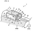
- the antenna structure 1 contains a surface-mounted antenna 2, a board-side control electrode 4 disposed on a mounting board 3 (a circuit board of a communication apparatus), a switch circuit 5, and a ground conductor 6.
- the surface-mounted antenna 2 is a ⁇ /4 transmission line type and is formed by a dielectric or magnetic base member 7, a radiating electrode 8, a ground electrode 9, a feeding electrode 10, and an antenna-side control electrode 11.
- the ground electrode 9 is disposed on a bottom surface 7b of the base member 7, and the radiating electrode 8 is arranged to extend from a side surface 7f to a top surface 7a.
- a first end of the radiating electrode 8 communicates and connects with the ground electrode 9, thus defining a ground end.
- a second end of the radiating electrode 8 defines an open end 8a. A portion of the open end 8a extends from the top surface 7a to the side surface 7d of the base member 7.
- a first end of the antenna-side control electrode 11 opposes the extended portion of the open end 8a with a gap therebetween.
- a capacitance is generated between the open end 8a of the radiating electrode 8 and the antenna-side control electrode 11.
- a second end of the antenna-side control electrode 11 is arranged such that it wraps around the side surface 7d to the bottom surface 7b of the base member 7.
- the second end of the antenna-side control electrode 11 opposes the ground electrode 9 with a gap therebetween.
- the antenna-side control electrode 11 electrically floats.
- the feeding electrode 10 is arranged to extend from the bottom surface 7b through the side surface 7d to the top surface 7a of the base member 7.
- a top end of the feeding electrode 10 opposes the open end 8a of the radiating electrode 8 with a gap therebetween.
- a second end of the feeding electrode 10 opposes the ground electrode 9 with a gap therebetween.
- a region in which the surface-mounted antenna 2 is mounted is a groundless portion in which the ground conductor 6 is not provided.
- the board-side control electrode 4, which electrically floats, and the switch circuit 5 are disposed on the groundless portion.
- a signal supply source 12 is disposed on the mounting board 3.
- a feeding wiring pattern 13 which is electrically connected with the signal supply source 12 is provided on the groundless portion.
- the surface-mounted antenna 2 is mounted on the groundless portion of the mounting board 3 so that the antenna-side control electrode 11 of the surface-mounted antenna 2 is electrically connected with the board-side control electrode 4 of the mounting board 3, so that the board-side control electrode 4 and the antenna-side control electrode 11 electrically float, and such that the feeding electrode 10 of the surface-mounted antenna 2 is electrically connected with the feeding wiring pattern 13 of the mounting board 3.
- Fig. 10B shows an equivalent circuit diagram of the antenna structure 1.
- L denotes the inductance of the radiating electrode 8
- R1 denotes the radiation resistance of the radiating electrode 8
- R2 denotes the internal resistance of the radiating electrode 8
- C1 denotes the capacitance between the open end 8a of the radiating electrode 8 and the antenna-side control electrode 11
- C2 denotes the capacitance between the open end 8a of the radiating electrode 8 and the feeding electrode
- C3 denotes the capacitance between the radiating electrode 8 and the ground.
- the capacitance C1 between the open end 8a of the radiating electrode 8 and the board-side control electrode 4 influences the resonant frequency of the radiating electrode 8.
- the switch circuit 5 is switched off, the capacitance C1 does not influence the resonant frequency of the radiating electrode 8. Accordingly, the influence of the capacitance C1 on the radiating electrode 8 varies according to whether or not the switch circuit 5 is switched on or off, and hence the resonant frequency of the radiating electrode 8 varies.
- the resonant frequency of the radiating electrode 8 can be easily changed by switching the switch circuit 5 on or off without changing the size and the shape of the radiating electrode 8 of the surface-mounted antenna 2 or the size of the base member 7.
- the structure of the switch circuit 5 is complex, and the switch circuit 5 is expensive. Thus, the antenna structure 1 is not commercially feasible.
- preferred embodiments of the present invention provide an antenna structure which has a simple configuration and which is capable of easily changing the resonant frequency of a radiating electrode without changing a surface-mounted antenna.
- preferred embodiments of the present invention provide a communication apparatus including such a novel antenna structure.
- an antenna structure includes a surface-mounted antenna including a radiating electrode disposed on a base member, the surface-mounted antenna being a ⁇ /4 transmission line type, a first end of the radiating electrode being a ground end and a second end of the radiating electrode being an open end, a mounting board on which the surface-mounted antenna is mounted, an antenna-side control electrode disposed on the base member of the surface-mounted antenna, the antenna-side control electrode having a capacitance generated between itself and the open end of the radiating electrode, a ground conductor disposed on the mounting board and which functions as ground, a board-side control electrode disposed on the mounting board, which is electrically connected with the antenna-side control electrode, and which electrically floats, and a resonant frequency adjuster having at least one of an inductance and a capacitance.
- the board-side control electrode is electrically connected with the ground conductor through the resonant frequency adjuster.
- the resonant frequency adjuster may include at least one of or a combination of at least two of a chip inductor component, a chip capacitor component, an inductor pattern, and a capacitor pattern.
- an antenna structure includes a surface-mounted antenna including a radiating electrode disposed on a base member, the surface-mounted antenna being a ⁇ /4 transmission line type, a first end of the radiating electrode being a ground end and a second end of the radiating electrode being an open end, a mounting board, on which the surface-mounted antenna is mounted, an antenna-side control electrode disposed on the base member of the surface-mounted antenna, the antenna-side control electrode having a capacitance that is generated between itself and the open end of the radiating electrode, a ground conductor disposed on the mounting board and which functions as ground, a board-side control electrode disposed on the mounting board, which is electrically connected with the antenna-side control electrode, and which electrically floats, and a resonant frequency adjuster including a solder bridge connecting the board-side control electrode and the ground conductor or a strip line.
- the board-side control electrode is electrically connected with the ground conductor at high frequencies through the resonant frequency adjuster.
- an antenna structure includes a surface-mounted antenna including a radiating electrode disposed on a base member, the surface-mounted antenna being a ⁇ /4 transmission line type, a first end of the radiating electrode being a ground end and a second end of the radiating electrode being an open end, a mounting board on which the surface-mounted antenna is mounted, an antenna-side control electrode disposed on the base member of the surface-mounted antenna, the antenna-side control electrode having a capacitance that is generated between itself and the open end of the radiating electrode, a ground conductor disposed on the mounting board and which functions as ground, a board-side control electrode disposed on the mounting board, which is electrically connected with the antenna-side control electrode and which electrically floats, a resonant frequency adjuster including a varicap diode, the board-side control electrode being electrically connected with the ground conductor at high frequencies through the resonant frequency adjuster, and a connection section connecting to a voltage supply source for applying a voltage to the
- a plurality of antenna-side control electrodes may be disposed on the base member of the surface-mounted antenna.
- Board-side control electrodes corresponding to the antenna-side control electrodes may be disposed on the mounting board.
- the board-side control electrodes may be electrically connected with the ground conductor at high frequencies through separate resonant frequency adjusters.
- a communication apparatus includes an antenna structure according to preferred embodiments of the present invention described above.
- the open end of the radiating electrode is connected at high frequencies to the ground conductor (ground) through the capacitance between the open end of the radiating electrode and the antenna-side control electrode, the antenna-side control electrode, the board-side control electrode, and the resonant frequency adjuster.
- the resonant frequency adjuster is preferably disposed on the mounting board.
- the resonant frequency adjuster may be defined by and include a chip inductor component, a chip capacitor component, an inductor pattern, a capacitor pattern, a solder bridge, a strip line, a varicap diode, or other suitable element. Since the configuration of such a component is much simpler than a switch circuit illustrated in a proposed example, the antenna structure can be simplified.
- an antenna structure is preferably constructed by mounting a ⁇ /4 transmission line type surface-mounted antenna on a mounting board.
- the impedance between an open end of a radiating electrode and ground is changed by a resonant frequency adjuster on the mounting board, thereby changing the resonant frequency of the radiating electrode. Accordingly, the resonant frequency of the radiating electrode can be easily changed without changing the surface-mounted antenna.
- the need to change the resonant frequency of the radiating electrode arises, the need can be immediately satisfied without devoting a large amount of time and labor to design the antenna structure.
- An increase in cost of the antenna structure due to the design is therefore minimized, and hence the antenna can be provided at a low cost. Since the configuration of the resonant frequency adjuster can be simplified, complications in the design, manufacture and performance of the antenna structure are reliably prevented.
- the cost of the communication apparatus can be reduced since the antenna structure is simple and the cost of the antenna is reduced.
- a plurality of antenna-side control electrodes is disposed on the surface-mounted antenna.
- Board-side control electrodes corresponding to the antenna-side control electrodes are disposed on the mounting board.
- the board-side control electrodes are electrically connected with a ground conductor at high frequencies through separate resonant frequency adjusters. The impedance between the open end of the radiating electrode and the ground can be finely adjusted by each resonant frequency adjuster. Accordingly, it becomes even easier to adjust the resonant frequency of the radiating electrode.
- Fig. 1 schematically shows an antenna structure, which is a feature of a communication apparatus according to a first preferred embodiment of the present invention.
- the communication apparatus can have various configurations.
- the configuration of the communication apparatus excluding the antenna structure which is described below, can have any configuration.
- a description of the communication apparatus excluding the antenna structure is omitted.
- An antenna structure 1 of the first preferred embodiment has a feature in that a board-side control electrode 4 on a mounting board 3 and a ground conductor 6 are electrically connected with each other at high frequencies through a resonant frequency adjuster 15.
- the remaining configuration is substantially similar to that of a proposed example shown in Fig. 10A.
- the same reference numerals are assigned to elements corresponding to those of the proposed example, and descriptions of the common elements are omitted.
- the resonant frequency adjuster 15 has at least one of an inductance and a capacitance.
- the equivalent circuit of the antenna structure 1 of the first preferred embodiment is shown in a circuit diagram of Fig. 2.
- a surface-mounted antenna 2 is a ⁇ /4 transmission line type, and the equivalent circuit of the surface-mounted antenna 2 is similar to that of the proposed example shown in Fig. 10B.
- a capacitance C1 between an open end 8a of a radiating electrode 8 and an antenna-side control electrode 11 is grounded through the inductance or capacitance of the resonant frequency adjuster 15.
- the capacitance C1 and an impedance due to the inductance or the capacitance of the resonant frequency adjuster 15 are provided between the open end 8a of the radiating electrode 8 and the ground.
- the impedance between the open end 8a of the radiating electrode 8 and the ground is changed.
- the resonant frequency of the radiating electrode 8 changes.
- the resonant frequency adjuster 15 has a capacitance, as shown by a graph of Fig. 3, as the capacitance increases, the more the resonant frequency of the radiating electrode 8 decreases.
- the resonant frequency adjuster 15 has an inductance, as the inductance increases, the resonant frequency of the radiating electrode 8 increases slightly.
- the resonant frequency adjuster 15 which has at least one of the inductance and the capacitance, can have various configurations. Although the resonant frequency adjusting device 15 can have any of these configurations, a few specific configurations will be now described.
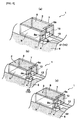
- Fig. 4A shows an example of the resonant frequency adjuster 15 including a chip component 17, such as a chip capacitor component or a chip inductor component.
- the chip component 17 has a predetermined constant, such as a capacitance of about 1 pF or a capacitance of about 2 pF.
- the resonant frequency adjuster 15 includes a chip component 18.
- the chip component 18 is arranged such that the inductance or the capacitance (high frequency impedance) thereof can be changed continuously or stepwisely.
- the chip component 18 includes a varicap or a trimmer capacitor.
- the resonant frequency of the radiating electrode 8 can be easily changed without using a plurality of types of chip components having different constants by simply changing the high frequency impedance of the chip component 18.
- the capacitance can be continuously changed.
- the resonant frequency of the radiating electrode 8 can be continuously changed. It becomes even easier to adjust the resonant frequency to a desired resonant frequency.
- the resonant frequency adjuster 15 includes a circuit pattern 20 which has at least one of a capacitor pattern and an inductor pattern.
- the capacitance or the inductance can be changed.
- the resonant frequency of the radiating electrode 8 can be changed.
- the resonant frequency adjuster 15, which includes the circuit pattern 20 can be disposed on the mounting board 3 together with the ground conductor 6 and a feeding wiring pattern 13 using film formation technology.
- the circuit pattern 20 functioning as the resonant frequency adjuster 15 can have various shapes.
- the shape shown in Fig. 5 is only an example, and the shape of the circuit pattern 20 is not limited to that shown in Fig. 5.
- the resonant frequency adjuster 15 which has at least one of the capacitance and the inductance.
- the configuration of the resonant frequency adjuster 15 is not limited to those shown in Figs. 4A, 4B, and 5.
- the resonant frequency adjuster 15 may preferably include a combination of at least two of the chip component 17, the chip component 18, and the circuit pattern 20.
- the resonant frequency adjuster 15 for changing the resonant frequency of the radiating electrode 8 by changing the impendence between the open end 8a of the radiating electrode 8 and the ground is provided on the mounting board 3.
- the resonant frequency of the radiating electrode 8 can be changed without changing the size of a base member 7 of the surface-mounted antenna 2 or without changing the shape of the radiating electrode 8.
- the need to change the resonant frequency can be immediately satisfied without devoting a large amount of time and labor to design the antenna structure 1.
- the cost of the antenna structure 1 is greatly reduced.
- the configuration of the resonant frequency adjuster 15 is simplified.
- the configuration of the antenna structure 1 can be simplified.
- the resonant frequency adjuster 15 is disposed between the board-side control electrode 4 and the ground conductor 6. Unlike the first preferred embodiment, the resonant frequency adjuster 15 of the second preferred embodiment changes the resonant frequency of the radiating electrode 8 by providing a capacitance between the board-side control electrode 4 and the ground conductor 6 or by directly electrically connecting the board-control electrode 4 with the ground conductor 6.
- the configuration excluding the resonant frequency adjuster 15 is substantially similar to that of the first preferred embodiment.
- the same reference numerals are given to elements corresponding to those of the first preferred embodiment, and descriptions of the common elements are omitted.
- the resonant frequency adjuster 15 can have configurations shown in Figs. 6A to 6C.
- the board-side control electrode 4 and the ground conductor 6 have protrusions 4a and 6a, respectively, at opposing portions thereof.
- the protrusions 4a and 6a define a capacitor pattern.
- a solder bridge 21 is arranged to extend across the protrusions 4a and 6a.
- the solder bridge 21 is arranged to directly electrically connect the board-side control electrode 4 with the ground conductor 6. Second, without providing the solder bridge 21, the capacitance of the capacitor pattern defined by the protrusions 4a and 6a of the board-side control electrode 4 and the ground conductor 6 is provided.
- the resonant frequency adjuster 15 includes a capacitor 23 that is formed by cutting off a strip line 22 shown in Fig. 6C.
- the strip line 22 can directly electrically connect the board-side control electrode 4 with the ground conductor 6, and the strip line 22 can be cut off to form the capacitance of the capacitor 23, thereby changing the resonant frequency of the radiating electrode 8.
- the amount of the strip line 22 cut off can be changed to change the capacitance of the capacitor 23, thereby changing the resonant frequency of the radiating electrode 8.
- the impedance between the open end 8a of the radiating electrode 8 and the ground can be changed by the resonant frequency adjuster 15 on the mounting board 3.
- the resonant frequency of the radiating electrode 8 can be easily changed without changing the surface-mounted antenna 2.
- the configuration of the resonant frequency adjuster 15 is simple, and complication of the antenna structure 1 is prevented.
- the surface-mounted antenna 2 has a plurality of antenna-side control electrodes 11 (11a and 11b), which preferably includes two in an example shown in Fig. 7A.
- the mounting board 3 has board-side control electrodes 4 (4a and 4b) corresponding to the antenna-side control electrodes 11 (11a and 11b).
- the board-side control electrodes 4a and 4b are connected at high frequencies to the ground conductor 6 through separate resonant frequency adjusters 15 (15a and 15b).
- the resonant frequency adjusters 15a and 15b each have the configuration illustrated in the first preferred embodiment or the preferred second embodiment.
- the equivalent circuit of the antenna structure 1 of the third preferred embodiment is shown in a circuit diagram of Fig. 7B.
- the impedance between the open end 8a of the radiating electrode 8 and the ground is changed by changing the capacitance or the inductance of each resonant frequency adjuster 15, by providing the solder bridge 21, or by cutting off the strip line 22.
- the resonant frequency of the radiating electrode 8 can be changed.
- the resonant frequency of the radiating electrode 8 can be easily changed without changing the surface-mounted antenna 2. Since a plurality of resonant frequency adjusters 15 is provided, the resonant frequency of the radiating electrode 8 can be finely adjusted.
- the present invention is not limited to the foregoing preferred embodiments and can be implemented in various other embodiments.
- the radiating electrode 8 is preferably strip-shaped in the foregoing preferred embodiments, the shape of the radiating electrode 8 is not limited to a strip.
- the shape of the radiating electrode 8 can be meandering or another suitable shape.
- the radiating electrode 8 is disposed on the surface of the base member 7, the location at which the radiating electrode 8 is provided can be appropriately determined.
- the radiating electrode 8 can be set in the interior of the base member 7. The location at which the radiating electrode 8 is provided is not limited to specific locations.
- only one base-side control electrode 4 is provided on a high-frequency-signal conduction path extending from the antenna-side control electrode 11 to the ground conductor 6.
- a plurality of board-side control electrodes 4 (4a to 4c) can be provided on the high-frequency-signal conduction path.
- the adjacent board-side control electrodes 4 are electrically connected with each other at high frequencies through the resonant frequency adjuster 15 similar to those shown in the foregoing preferred embodiments. Accordingly, the number of the resonant frequency adjusters 15 increases, and hence the resonant frequency of the radiating electrode 8 can be finely adjusted in a simple manner.
- the resonant frequency adjuster 15 may preferably include a varicap diode.
- a connection section X for connecting to a voltage supply source Vc for applying a voltage to the varicap diode is provided.
- the resonant frequency of the radiating electrode 8 can be changed.
- Fig. 9 shows an example of a return loss characteristic indicating the relationship between the voltage applied to the varicap diode and the resonant frequency of the radiating electrode 8. The example of the return loss characteristic is obtained when the antenna structure 1 is constructed as shown in Fig. 8A and when the equivalent circuit of the antenna structure 1 is such as that shown in Fig. 8B.
- a resonant frequency adjuster 15a shown in Fig. 8A has a capacitance Ca.
- a resonant frequency adjuster 15b is a varicap diode.
- a resonant frequency adjuster 15c has an inductance Lc.
- a resonant frequency adjuster 15d has a capacitance Cd.
- the board-side control electrode 4c has a connection section X for connecting to the voltage supply source Vc for applying a voltage to the varicap diode.
- solid line A indicates a return loss characteristic when a voltage of 1 V is applied to the varicap diode
- dotted line B indicates a return loss characteristic when a voltage of 2 V is applied to the varicap diode
- dotted and dashed line C indicates a return loss characteristic when a voltage of 3 v is applied to the varicap diode.
- two board-side control electrodes 4 and two antenna-side control electrodes 11 are preferably provided.
- the number of the board-side control electrodes 4 and the number of the antenna-side control electrodes 11 can be three or greater and the number thereof is not limited.
Landscapes
- Engineering & Computer Science (AREA)
- Microelectronics & Electronic Packaging (AREA)
- Computer Networks & Wireless Communication (AREA)
- Support Of Aerials (AREA)
- Waveguide Aerials (AREA)
- Details Of Aerials (AREA)
Abstract
Description
Claims (11)
- An antenna structure (1) comprising:a surface-mounted antenna (2) including a base member (7) and a radiating electrode (8) disposed on said base member (7), the surface-mounted antenna (2) being a λ/4 transmission line type, a first end of the radiating electrode (8) being a ground end and a second end of the radiating electrode being an open end;a mounting board (3) on which the surface-mounted antenna (2) is mounted;an antenna-side control electrode (11) disposed on the base member (7) of the surface-mounted antenna (2), the antenna-side control electrode (11) having a capacitance between itself and the open end (8a) of the radiating electrode (8);a ground conductor (6) disposed on the mounting board (3) and defining a ground;a board-side control electrode (4) disposed on the mounting board (3), which is electrically connected with the antenna-side control electrode (11), and which electrically floats; anda resonant frequency adjusting member (15) having at least one of an inductance and a capacitance, the board-side control electrode (4) being electrically connected with the ground conductor (6) through the resonant frequency adjusting member (15).
- An antenna structure (1) according to claim 1, wherein the resonant frequency adjusting member (15) includes at least one of a chip inductor component (17,18), a chip capacitor component (17,18), an inductor pattern (20), and a capacitor pattern (20).
- An antenna structure (1) according to claim 1, wherein the resonant frequency adjusting member (15) includes a combination of at least two of a chip inductor component (17,18), a chip capacitor component (17,18), an inductor pattern (20), and a capacitor pattern (20).
- An antenna structure (1) according to one of claims 1 to 3, wherein the capacitance between the open end (8a) of the radiating electrode (8) and the antenna-side control electrode (11) is grounded through the at least one of the inductance and capacitance of the resonant frequency adjusting member (15).
- An antenna structure (1) according to one of claims 1 to 4, wherein the capacitance of the antenna side control electrode (11) and an impedance due to the at least one of the inductance and the capacitance of the resonant frequency adjusting member (15) are provided between the open end (8a) of the radiating electrode (8) and the ground.
- An antenna structure (1) comprising:a surface-mounted antenna including a base member (7) and a radiating electrode (8) disposed on said base member (7), the surface-mounted antenna being a λ/4 transmission line type, a first end of the radiating electrode (8) being a ground end and a second end (8a) of the radiating electrode (8) being an open end;a mounting board (3) on which the surface-mounted antenna (2) is mounted;an antenna-side control electrode (11) disposed on the base member (7) of the surface-mounted antenna (2), the antenna-side control electrode (11) having a capacitance between itself and the open end (8a) of the radiating electrode (8);a ground conductor (6) disposed on the mounting board (3) and defining a ground;a board-side control electrode (4) disposed on the mounting board (3), which is electrically connected with the antenna-side control electrode (11), and which electrically floats; anda resonant frequency adjusting member (15) including a solder bridge (21) connecting the board-side control electrode (4) and one of the ground conductor (6) or a strip line (22), the board-side control electrode (4) being electrically connected with the ground conductor (6) at high frequencies through the resonant frequency adjusting member (15).
- An antenna structure (1) according to claim 6, wherein the board-side control electrode (4) and the ground conductor (6) have protrusions and the protrusions define a capacitor pattern (20).
- An antenna structure (1) according to claim 7, wherein the solder bridge (11) is arranged to extend across the protrusions.
- An antenna structure (1) comprising:a surface-mounted antenna (2) including a base member (7) and a radiating electrode (8) disposed on said base member (7), the surface-mounted antenna (2) being a λ/4 transmission line type, a first end of the radiating electrode(8) being a ground end and a second end (8a) of the radiating electrode (8) being an open end;a mounting board (3) on which the surface-mounted antenna (2) is mounted;an antenna-side control electrode (11) disposed on the base member (7) of the surface-mounted antenna (2), the antenna-side control electrode (11) having a capacitance between itself and the open end (8a) of the radiating electrode (8);a ground conductor (6) disposed on the mounting board (3) and defining a ground;a board-side control electrode (4) disposed on the mounting board (3), which is electrically connected with the antenna-side control electrode (11), and which electrically floats;a resonant frequency adjusting member (15) including a varicap diode (15b), the board-side control electrode (4) being electrically connected with the ground conductor (6) at high frequencies through the resonant frequency adjusting member (15); anda connection section connecting (x) to a voltage supply source (Vc) for applying a voltage to the varicap diode (15).
- An antenna structure (1) according to any of the preceding cliams, wherein a plurality of antenna-side control electrodes (11a, 11b) are disposed on the base member (7) of the surface-mounted antenna (2);board-side control electrodes (4a, 4b) corresponding to the antenna-side control electrodes (11a, 11b) are disposed on the mounting board (3); andthe board-side control electrodes (4a,4b) are electrically connected with the ground conductor (6) at high frequencies through separate resonant frequency adjusting members (15a,15b).
- A communication apparatus comprising an antenna structure as set forth in any of the preceding claims.
Priority Applications (1)
| Application Number | Priority Date | Filing Date | Title |
|---|---|---|---|
| EP04013179A EP1453139A1 (en) | 2001-05-08 | 2002-04-25 | Method for adjusting the resonant frequency of an antenna structure |
Applications Claiming Priority (2)
| Application Number | Priority Date | Filing Date | Title |
|---|---|---|---|
| JP2001137571 | 2001-05-08 | ||
| JP2001137571A JP2002335117A (en) | 2001-05-08 | 2001-05-08 | Antenna structure and communication device equipped therewith |
Related Child Applications (1)
| Application Number | Title | Priority Date | Filing Date |
|---|---|---|---|
| EP04013179A Division EP1453139A1 (en) | 2001-05-08 | 2002-04-25 | Method for adjusting the resonant frequency of an antenna structure |
Publications (2)
| Publication Number | Publication Date |
|---|---|
| EP1256998A2 true EP1256998A2 (en) | 2002-11-13 |
| EP1256998A3 EP1256998A3 (en) | 2004-01-07 |
Family
ID=18984664
Family Applications (2)
| Application Number | Title | Priority Date | Filing Date |
|---|---|---|---|
| EP04013179A Withdrawn EP1453139A1 (en) | 2001-05-08 | 2002-04-25 | Method for adjusting the resonant frequency of an antenna structure |
| EP02009490A Withdrawn EP1256998A3 (en) | 2001-05-08 | 2002-04-25 | Antenna structure and communication apparatus including the same |
Family Applications Before (1)
| Application Number | Title | Priority Date | Filing Date |
|---|---|---|---|
| EP04013179A Withdrawn EP1453139A1 (en) | 2001-05-08 | 2002-04-25 | Method for adjusting the resonant frequency of an antenna structure |
Country Status (4)
| Country | Link |
|---|---|
| US (1) | US6614398B2 (en) |
| EP (2) | EP1453139A1 (en) |
| JP (1) | JP2002335117A (en) |
| CN (1) | CN1386031A (en) |
Cited By (5)
| Publication number | Priority date | Publication date | Assignee | Title |
|---|---|---|---|---|
| EP1482592A1 (en) * | 2003-05-29 | 2004-12-01 | Sony Corporation | A surface mount antenna, and an antenna element mounting method |
| WO2005011055A1 (en) * | 2003-07-24 | 2005-02-03 | Koninklijke Philips Electronics N.V. | Tuning improvements in “inverted-l” planar antennas |
| WO2006114771A1 (en) * | 2005-04-27 | 2006-11-02 | Nxp B.V. | Radio device having antenna arrangement suited for operating over a plurality of bands. |
| EP1734659A1 (en) * | 2005-06-07 | 2006-12-20 | Hitachi, Ltd. | Antenna with controllable resonance frequency for wireless communication |
| CN113015315A (en) * | 2021-02-22 | 2021-06-22 | 深圳拓邦股份有限公司 | Circuit board capable of improving wiring overcurrent capacity and manufacturing method thereof |
Families Citing this family (80)
| Publication number | Priority date | Publication date | Assignee | Title |
|---|---|---|---|---|
| GB2383471A (en) * | 2001-12-19 | 2003-06-25 | Harada Ind | High-bandwidth multi-band antenna |
| JP2003198410A (en) * | 2001-12-27 | 2003-07-11 | Matsushita Electric Ind Co Ltd | Antenna for communication terminal equipment |
| KR100533624B1 (en) * | 2002-04-16 | 2005-12-06 | 삼성전기주식회사 | Multi band chip antenna with dual feeding port, and mobile communication apparatus using the same |
| KR100616509B1 (en) * | 2002-05-31 | 2006-08-29 | 삼성전기주식회사 | Broadband chip antenna |
| AU2003281402A1 (en) * | 2002-07-05 | 2004-01-23 | Taiyo Yuden Co., Ldt. | Dielectric antenna, antenna-mounted substrate, and mobile communication machine having them therein |
| JP3794360B2 (en) * | 2002-08-23 | 2006-07-05 | 株式会社村田製作所 | Antenna structure and communication device having the same |
| JP3739740B2 (en) * | 2002-11-28 | 2006-01-25 | 京セラ株式会社 | Surface mount antenna and antenna device |
| JP4192782B2 (en) * | 2003-07-10 | 2008-12-10 | Toto株式会社 | High frequency sensor and antenna device |
| JP4458780B2 (en) * | 2003-07-11 | 2010-04-28 | シチズン電子株式会社 | Antenna device for radio clock |
| JP4263972B2 (en) * | 2003-09-11 | 2009-05-13 | 京セラ株式会社 | Surface mount antenna, antenna device, and wireless communication device |
| JP2005109636A (en) | 2003-09-29 | 2005-04-21 | Matsushita Electric Ind Co Ltd | Portable radio |
| EP1978595B1 (en) * | 2003-12-25 | 2011-03-23 | Mitsubishi Materials Corporation | Antenna device and communication apparatus |
| JP4192781B2 (en) * | 2003-12-26 | 2008-12-10 | Toto株式会社 | ANTENNA DEVICE AND HIGH FREQUENCY SENSOR |
| US20110215985A1 (en) * | 2004-06-10 | 2011-09-08 | Raysat Antenna Systems, L.L.C. | Applications for Low Profile Two Way Satellite Antenna System |
| JP2006314005A (en) * | 2005-05-09 | 2006-11-16 | Nippon Antenna Co Ltd | Built-in antenna |
| CN101171721B (en) * | 2005-05-11 | 2013-01-23 | 株式会社村田制作所 | Antenna structure, and radio communication device having the structure |
| GB2439863C (en) * | 2005-05-13 | 2009-04-08 | Murata Manufacturing Co | Antenna structure and wireless communication device including the same |
| FI20055420A0 (en) | 2005-07-25 | 2005-07-25 | Lk Products Oy | Adjustable multi-band antenna |
| FI119009B (en) | 2005-10-03 | 2008-06-13 | Pulse Finland Oy | Multiple-band antenna |
| FI118782B (en) | 2005-10-14 | 2008-03-14 | Pulse Finland Oy | Adjustable antenna |
| US8618990B2 (en) | 2011-04-13 | 2013-12-31 | Pulse Finland Oy | Wideband antenna and methods |
| EP2048739A4 (en) * | 2006-07-28 | 2009-08-05 | Murata Manufacturing Co | Antenna device and radio communication device |
| JPWO2008035526A1 (en) * | 2006-09-20 | 2010-01-28 | 株式会社村田製作所 | Antenna structure and radio communication apparatus using the same |
| KR100799875B1 (en) * | 2006-11-22 | 2008-01-30 | 삼성전기주식회사 | Chip antenna and mobile terminal including the same |
| US7345638B1 (en) * | 2006-12-18 | 2008-03-18 | Motorola Inc | Communications assembly and antenna radiator assembly |
| DE112008000578B4 (en) * | 2007-03-23 | 2014-05-22 | Murata Mfg. Co., Ltd. | Antenna and radio communication device |
| FI20075269A0 (en) | 2007-04-19 | 2007-04-19 | Pulse Finland Oy | Method and arrangement for antenna matching |
| KR100867507B1 (en) * | 2007-07-12 | 2008-11-07 | 삼성전기주식회사 | Chip antenna |
| JP4991451B2 (en) * | 2007-08-29 | 2012-08-01 | 京セラ株式会社 | Antenna, method for adjusting resonance frequency thereof, and communication apparatus using the same |
| FI120427B (en) | 2007-08-30 | 2009-10-15 | Pulse Finland Oy | Adjustable multiband antenna |
| JP4941202B2 (en) * | 2007-09-26 | 2012-05-30 | Tdk株式会社 | Antenna device and characteristic adjustment method thereof |
| JP4924327B2 (en) * | 2007-09-26 | 2012-04-25 | Tdk株式会社 | Antenna device and characteristic adjustment method thereof |
| CN101836329B (en) * | 2007-10-26 | 2012-12-19 | Tdk株式会社 | Antenna device and wireless communication equipment using the same |
| JP5018488B2 (en) * | 2008-01-15 | 2012-09-05 | Tdk株式会社 | Antenna module |
| JP4784636B2 (en) * | 2008-10-28 | 2011-10-05 | Tdk株式会社 | Surface mount antenna, antenna device using the same, and radio communication device |
| JP4788791B2 (en) * | 2009-02-27 | 2011-10-05 | Tdk株式会社 | Antenna device |
| JP5251610B2 (en) * | 2009-03-03 | 2013-07-31 | Tdk株式会社 | ANTENNA DEVICE AND ANTENNA ELEMENT USED FOR THE SAME |
| JP5403059B2 (en) * | 2009-08-27 | 2014-01-29 | 株式会社村田製作所 | Flexible substrate antenna and antenna device |
| FI20096134A0 (en) | 2009-11-03 | 2009-11-03 | Pulse Finland Oy | Adjustable antenna |
| JP2011109568A (en) * | 2009-11-20 | 2011-06-02 | Tdk Corp | Antenna device |
| FI20096251A0 (en) | 2009-11-27 | 2009-11-27 | Pulse Finland Oy | MIMO antenna |
| JP5120367B2 (en) * | 2009-12-09 | 2013-01-16 | Tdk株式会社 | Antenna device |
| US8847833B2 (en) | 2009-12-29 | 2014-09-30 | Pulse Finland Oy | Loop resonator apparatus and methods for enhanced field control |
| FI20105158A7 (en) | 2010-02-18 | 2011-08-19 | Pulse Finland Oy | ANTENNA EQUIPPED WITH SHELL RADIATOR |
| US9406998B2 (en) | 2010-04-21 | 2016-08-02 | Pulse Finland Oy | Distributed multiband antenna and methods |
| WO2012039210A1 (en) * | 2010-09-22 | 2012-03-29 | アルプス電気株式会社 | Electronic device |
| FI20115072A0 (en) | 2011-01-25 | 2011-01-25 | Pulse Finland Oy | Multi-resonance antenna, antenna module and radio unit |
| US8648752B2 (en) | 2011-02-11 | 2014-02-11 | Pulse Finland Oy | Chassis-excited antenna apparatus and methods |
| US9673507B2 (en) | 2011-02-11 | 2017-06-06 | Pulse Finland Oy | Chassis-excited antenna apparatus and methods |
| US8866689B2 (en) | 2011-07-07 | 2014-10-21 | Pulse Finland Oy | Multi-band antenna and methods for long term evolution wireless system |
| US9450291B2 (en) | 2011-07-25 | 2016-09-20 | Pulse Finland Oy | Multiband slot loop antenna apparatus and methods |
| JP2013078027A (en) * | 2011-09-30 | 2013-04-25 | Tdk Corp | Patch antenna |
| US9123990B2 (en) | 2011-10-07 | 2015-09-01 | Pulse Finland Oy | Multi-feed antenna apparatus and methods |
| US9531058B2 (en) | 2011-12-20 | 2016-12-27 | Pulse Finland Oy | Loosely-coupled radio antenna apparatus and methods |
| US9484619B2 (en) | 2011-12-21 | 2016-11-01 | Pulse Finland Oy | Switchable diversity antenna apparatus and methods |
| JP5545303B2 (en) * | 2012-01-16 | 2014-07-09 | Tdk株式会社 | Antenna device |
| US8988296B2 (en) | 2012-04-04 | 2015-03-24 | Pulse Finland Oy | Compact polarized antenna and methods |
| TW201345050A (en) * | 2012-04-27 | 2013-11-01 | Univ Nat Taiwan Science Tech | Dual band antenna with circular polarization |
| KR101905769B1 (en) * | 2012-06-29 | 2018-12-05 | 엘지이노텍 주식회사 | Antenna and the method for manufacturing the same |
| TWI532259B (en) * | 2012-08-27 | 2016-05-01 | 鴻海精密工業股份有限公司 | Broadband antenna element |
| US9979078B2 (en) | 2012-10-25 | 2018-05-22 | Pulse Finland Oy | Modular cell antenna apparatus and methods |
| US10069209B2 (en) | 2012-11-06 | 2018-09-04 | Pulse Finland Oy | Capacitively coupled antenna apparatus and methods |
| US10079428B2 (en) | 2013-03-11 | 2018-09-18 | Pulse Finland Oy | Coupled antenna structure and methods |
| US9647338B2 (en) | 2013-03-11 | 2017-05-09 | Pulse Finland Oy | Coupled antenna structure and methods |
| US9634383B2 (en) | 2013-06-26 | 2017-04-25 | Pulse Finland Oy | Galvanically separated non-interacting antenna sector apparatus and methods |
| JP6145388B2 (en) * | 2013-10-30 | 2017-06-14 | 日本電産サンキョー株式会社 | Contactless communication module and card reader |
| TWM475708U (en) * | 2013-11-14 | 2014-04-01 | Unictron Tech Corporation | Multi-frequency antenna device |
| US9680212B2 (en) | 2013-11-20 | 2017-06-13 | Pulse Finland Oy | Capacitive grounding methods and apparatus for mobile devices |
| US9590308B2 (en) | 2013-12-03 | 2017-03-07 | Pulse Electronics, Inc. | Reduced surface area antenna apparatus and mobile communications devices incorporating the same |
| US9350081B2 (en) | 2014-01-14 | 2016-05-24 | Pulse Finland Oy | Switchable multi-radiator high band antenna apparatus |
| US9948002B2 (en) | 2014-08-26 | 2018-04-17 | Pulse Finland Oy | Antenna apparatus with an integrated proximity sensor and methods |
| US9973228B2 (en) | 2014-08-26 | 2018-05-15 | Pulse Finland Oy | Antenna apparatus with an integrated proximity sensor and methods |
| US9722308B2 (en) | 2014-08-28 | 2017-08-01 | Pulse Finland Oy | Low passive intermodulation distributed antenna system for multiple-input multiple-output systems and methods of use |
| US10320068B2 (en) * | 2014-12-22 | 2019-06-11 | Huawei Technologies Co., Ltd. | Antenna and terminal |
| US9906260B2 (en) | 2015-07-30 | 2018-02-27 | Pulse Finland Oy | Sensor-based closed loop antenna swapping apparatus and methods |
| CN111183554B (en) * | 2017-10-03 | 2021-09-17 | 株式会社村田制作所 | Antenna module and method for inspecting antenna module |
| US10877612B2 (en) * | 2018-02-14 | 2020-12-29 | Continental Automotive Systems, Inc. | Capacitive touch/proximity sensor with integrated ultra-high frequency antenna |
| KR102728514B1 (en) * | 2018-11-27 | 2024-11-12 | 삼성전자주식회사 | Living body information detecting apparatus |
| JP7702776B2 (en) * | 2020-03-03 | 2025-07-04 | 日東電工株式会社 | Wiring Circuit Board |
| US20230369771A1 (en) * | 2022-05-10 | 2023-11-16 | Te Connectivity Solutions Gmbh | Antenna assembly for electrical device |
Family Cites Families (11)
| Publication number | Priority date | Publication date | Assignee | Title |
|---|---|---|---|---|
| JP3216588B2 (en) * | 1996-11-21 | 2001-10-09 | 株式会社村田製作所 | Antenna device |
| JP3307248B2 (en) | 1996-12-09 | 2002-07-24 | 株式会社村田製作所 | Surface mounted antenna and surface mounted antenna device |
| JP3279205B2 (en) * | 1996-12-10 | 2002-04-30 | 株式会社村田製作所 | Surface mount antenna and communication equipment |
| FI113212B (en) * | 1997-07-08 | 2004-03-15 | Nokia Corp | Dual resonant antenna design for multiple frequency ranges |
| JPH11136025A (en) * | 1997-08-26 | 1999-05-21 | Murata Mfg Co Ltd | Frequency switching type surface mounting antenna, antenna device using the antenna and communication unit using the antenna device |
| JP3663888B2 (en) * | 1998-03-02 | 2005-06-22 | 株式会社村田製作所 | Surface mount antenna and communication device equipped with the same |
| JP3246440B2 (en) * | 1998-04-28 | 2002-01-15 | 株式会社村田製作所 | Antenna device and communication device using the same |
| EP1014487A1 (en) * | 1998-12-23 | 2000-06-28 | Sony International (Europe) GmbH | Patch antenna and method for tuning a patch antenna |
| JP2001053543A (en) * | 1999-08-12 | 2001-02-23 | Sony Corp | Antenna device |
| CN1141756C (en) * | 1999-09-30 | 2004-03-10 | 株式会社村田制作所 | Surface-mount antenna and communication device with surface-mount antenna |
| JP3646782B2 (en) * | 1999-12-14 | 2005-05-11 | 株式会社村田製作所 | ANTENNA DEVICE AND COMMUNICATION DEVICE USING THE SAME |
-
2001
- 2001-05-08 JP JP2001137571A patent/JP2002335117A/en active Pending
-
2002
- 2002-04-15 US US10/121,733 patent/US6614398B2/en not_active Expired - Lifetime
- 2002-04-25 EP EP04013179A patent/EP1453139A1/en not_active Withdrawn
- 2002-04-25 EP EP02009490A patent/EP1256998A3/en not_active Withdrawn
- 2002-05-08 CN CN02119312A patent/CN1386031A/en active Pending
Cited By (13)
| Publication number | Priority date | Publication date | Assignee | Title |
|---|---|---|---|---|
| US7034752B2 (en) | 2003-05-29 | 2006-04-25 | Sony Corporation | Surface mount antenna, and an antenna element mounting method |
| EP1482592A1 (en) * | 2003-05-29 | 2004-12-01 | Sony Corporation | A surface mount antenna, and an antenna element mounting method |
| US7843397B2 (en) | 2003-07-24 | 2010-11-30 | Epcos Ag | Tuning improvements in “inverted-L” planar antennas |
| WO2005011055A1 (en) * | 2003-07-24 | 2005-02-03 | Koninklijke Philips Electronics N.V. | Tuning improvements in “inverted-l” planar antennas |
| KR101143731B1 (en) * | 2003-07-24 | 2012-05-09 | 에프코스 아게 | Tuning improvements in ?inverted-l? planar antennas |
| US7990319B2 (en) | 2005-04-27 | 2011-08-02 | Epcos Ag | Radio device having antenna arrangement suited for operating over a plurality of bands |
| WO2006114771A1 (en) * | 2005-04-27 | 2006-11-02 | Nxp B.V. | Radio device having antenna arrangement suited for operating over a plurality of bands. |
| US7714787B2 (en) | 2005-06-07 | 2010-05-11 | Hitachi, Ltd. | Antenna, and wireless module, wireless unit and wireless apparatus having the antenna |
| US7817094B2 (en) | 2005-06-07 | 2010-10-19 | Hitachi, Ltd. | Antenna, and wireless module, wireless unit and wireless apparatus having the antenna |
| EP1852979A3 (en) * | 2005-06-07 | 2007-11-21 | Hitachi, Ltd. | Wireless unit having an antenna with controllable resonance frequency |
| EP1734659A1 (en) * | 2005-06-07 | 2006-12-20 | Hitachi, Ltd. | Antenna with controllable resonance frequency for wireless communication |
| CN113015315A (en) * | 2021-02-22 | 2021-06-22 | 深圳拓邦股份有限公司 | Circuit board capable of improving wiring overcurrent capacity and manufacturing method thereof |
| CN113015315B (en) * | 2021-02-22 | 2022-07-19 | 深圳拓邦股份有限公司 | Circuit board capable of improving wiring overcurrent capacity and manufacturing method thereof |
Also Published As
| Publication number | Publication date |
|---|---|
| US6614398B2 (en) | 2003-09-02 |
| EP1256998A3 (en) | 2004-01-07 |
| CN1386031A (en) | 2002-12-18 |
| US20020167448A1 (en) | 2002-11-14 |
| JP2002335117A (en) | 2002-11-22 |
| EP1453139A1 (en) | 2004-09-01 |
Similar Documents
| Publication | Publication Date | Title |
|---|---|---|
| US6614398B2 (en) | Antenna structure and communication apparatus including the same | |
| JP3684285B2 (en) | Tunable slot antenna | |
| US7119749B2 (en) | Antenna and radio communication apparatus | |
| US5959582A (en) | Surface mount type antenna and communication apparatus | |
| US5861854A (en) | Surface-mount antenna and a communication apparatus using the same | |
| US6600449B2 (en) | Antenna apparatus | |
| EP1102348B1 (en) | Surface mounting antenna and communication apparatus using the same antenna | |
| EP2226891B1 (en) | Antenna device and antenna element used therefor | |
| US7916086B2 (en) | Antenna component and methods | |
| EP2043196B1 (en) | Wireless communication apparatus | |
| EP0993070A1 (en) | Inverted-F antenna with switched impedance | |
| US8242970B2 (en) | Antenna apparatus | |
| US20040233109A1 (en) | Mobile communication device | |
| US20040085245A1 (en) | Surface mount antenna, antenna device using the same, and communication device | |
| EP1014487A1 (en) | Patch antenna and method for tuning a patch antenna | |
| JP2001284954A (en) | Surface mount antenna, frequency control and setting method for dual resonance therefor and communication equipment provided with surface mount antenna | |
| US7808435B2 (en) | Antenna structure and wireless communication apparatus including same | |
| JP2003158419A (en) | Inverted f antenna, and its feeding method and its antenna adjusting method | |
| US20240333320A1 (en) | Multi-Band Antenna for use with Limited Size Ground Planes | |
| JPH10173425A (en) | Surface mount antenna and antenna device and communication equipment | |
| JP4645603B2 (en) | Antenna structure and wireless communication apparatus including the same | |
| JPH1032413A (en) | Surface mounted antenna | |
| KR101926549B1 (en) | Antenna apparatus | |
| JP2002151930A (en) | Antenna structure and radio equipment provided with it | |
| KR101284128B1 (en) | Broadband combination meanderline and patch antenna |
Legal Events
| Date | Code | Title | Description |
|---|---|---|---|
| PUAI | Public reference made under article 153(3) epc to a published international application that has entered the european phase |
Free format text: ORIGINAL CODE: 0009012 |
|
| 17P | Request for examination filed |
Effective date: 20020425 |
|
| AK | Designated contracting states |
Kind code of ref document: A2 Designated state(s): AT BE CH CY DE DK ES FI FR GB GR IE IT LI LU MC NL PT SE TR |
|
| AX | Request for extension of the european patent |
Free format text: AL;LT;LV;MK;RO;SI |
|
| PUAL | Search report despatched |
Free format text: ORIGINAL CODE: 0009013 |
|
| AK | Designated contracting states |
Kind code of ref document: A3 Designated state(s): AT BE CH CY DE DK ES FI FR GB GR IE IT LI LU MC NL PT SE TR |
|
| AX | Request for extension of the european patent |
Extension state: AL LT LV MK RO SI |
|
| RIC1 | Information provided on ipc code assigned before grant |
Ipc: 7H 01Q 9/04 B Ipc: 7H 01Q 5/00 B Ipc: 7H 01Q 1/38 B Ipc: 7H 01Q 1/24 A |
|
| 17Q | First examination report despatched |
Effective date: 20040305 |
|
| AKX | Designation fees paid |
Designated state(s): DE FR GB |
|
| STAA | Information on the status of an ep patent application or granted ep patent |
Free format text: STATUS: THE APPLICATION HAS BEEN WITHDRAWN |
|
| 18W | Application withdrawn |
Effective date: 20041209 |