EP1256977A1 - Method and apparatus for producing polysilicon film, semiconductor device, and method of manufacture thereof - Google Patents
Method and apparatus for producing polysilicon film, semiconductor device, and method of manufacture thereof Download PDFInfo
- Publication number
- EP1256977A1 EP1256977A1 EP00964741A EP00964741A EP1256977A1 EP 1256977 A1 EP1256977 A1 EP 1256977A1 EP 00964741 A EP00964741 A EP 00964741A EP 00964741 A EP00964741 A EP 00964741A EP 1256977 A1 EP1256977 A1 EP 1256977A1
- Authority
- EP
- European Patent Office
- Prior art keywords
- laser
- silicon film
- polycrystal
- amorphous silicon
- irradiation
- Prior art date
- Legal status (The legal status is an assumption and is not a legal conclusion. Google has not performed a legal analysis and makes no representation as to the accuracy of the status listed.)
- Granted
Links
Images




Classifications
-
- G—PHYSICS
- G02—OPTICS
- G02F—OPTICAL DEVICES OR ARRANGEMENTS FOR THE CONTROL OF LIGHT BY MODIFICATION OF THE OPTICAL PROPERTIES OF THE MEDIA OF THE ELEMENTS INVOLVED THEREIN; NON-LINEAR OPTICS; FREQUENCY-CHANGING OF LIGHT; OPTICAL LOGIC ELEMENTS; OPTICAL ANALOGUE/DIGITAL CONVERTERS
- G02F1/00—Devices or arrangements for the control of the intensity, colour, phase, polarisation or direction of light arriving from an independent light source, e.g. switching, gating or modulating; Non-linear optics
- G02F1/01—Devices or arrangements for the control of the intensity, colour, phase, polarisation or direction of light arriving from an independent light source, e.g. switching, gating or modulating; Non-linear optics for the control of the intensity, phase, polarisation or colour
- G02F1/13—Devices or arrangements for the control of the intensity, colour, phase, polarisation or direction of light arriving from an independent light source, e.g. switching, gating or modulating; Non-linear optics for the control of the intensity, phase, polarisation or colour based on liquid crystals, e.g. single liquid crystal display cells
-
- C—CHEMISTRY; METALLURGY
- C23—COATING METALLIC MATERIAL; COATING MATERIAL WITH METALLIC MATERIAL; CHEMICAL SURFACE TREATMENT; DIFFUSION TREATMENT OF METALLIC MATERIAL; COATING BY VACUUM EVAPORATION, BY SPUTTERING, BY ION IMPLANTATION OR BY CHEMICAL VAPOUR DEPOSITION, IN GENERAL; INHIBITING CORROSION OF METALLIC MATERIAL OR INCRUSTATION IN GENERAL
- C23C—COATING METALLIC MATERIAL; COATING MATERIAL WITH METALLIC MATERIAL; SURFACE TREATMENT OF METALLIC MATERIAL BY DIFFUSION INTO THE SURFACE, BY CHEMICAL CONVERSION OR SUBSTITUTION; COATING BY VACUUM EVAPORATION, BY SPUTTERING, BY ION IMPLANTATION OR BY CHEMICAL VAPOUR DEPOSITION, IN GENERAL
- C23C14/00—Coating by vacuum evaporation, by sputtering or by ion implantation of the coating forming material
- C23C14/58—After-treatment
- C23C14/5806—Thermal treatment
- C23C14/5813—Thermal treatment using lasers
-
- B—PERFORMING OPERATIONS; TRANSPORTING
- B23—MACHINE TOOLS; METAL-WORKING NOT OTHERWISE PROVIDED FOR
- B23K—SOLDERING OR UNSOLDERING; WELDING; CLADDING OR PLATING BY SOLDERING OR WELDING; CUTTING BY APPLYING HEAT LOCALLY, e.g. FLAME CUTTING; WORKING BY LASER BEAM
- B23K26/00—Working by laser beam, e.g. welding, cutting or boring
- B23K26/02—Positioning or observing the workpiece, e.g. with respect to the point of impact; Aligning, aiming or focusing the laser beam
- B23K26/06—Shaping the laser beam, e.g. by masks or multi-focusing
- B23K26/0604—Shaping the laser beam, e.g. by masks or multi-focusing by a combination of beams
-
- B—PERFORMING OPERATIONS; TRANSPORTING
- B23—MACHINE TOOLS; METAL-WORKING NOT OTHERWISE PROVIDED FOR
- B23K—SOLDERING OR UNSOLDERING; WELDING; CLADDING OR PLATING BY SOLDERING OR WELDING; CUTTING BY APPLYING HEAT LOCALLY, e.g. FLAME CUTTING; WORKING BY LASER BEAM
- B23K26/00—Working by laser beam, e.g. welding, cutting or boring
- B23K26/02—Positioning or observing the workpiece, e.g. with respect to the point of impact; Aligning, aiming or focusing the laser beam
- B23K26/06—Shaping the laser beam, e.g. by masks or multi-focusing
- B23K26/073—Shaping the laser spot
- B23K26/0738—Shaping the laser spot into a linear shape
-
- B—PERFORMING OPERATIONS; TRANSPORTING
- B23—MACHINE TOOLS; METAL-WORKING NOT OTHERWISE PROVIDED FOR
- B23K—SOLDERING OR UNSOLDERING; WELDING; CLADDING OR PLATING BY SOLDERING OR WELDING; CUTTING BY APPLYING HEAT LOCALLY, e.g. FLAME CUTTING; WORKING BY LASER BEAM
- B23K26/00—Working by laser beam, e.g. welding, cutting or boring
- B23K26/08—Devices involving relative movement between laser beam and workpiece
- B23K26/083—Devices involving movement of the workpiece in at least one axial direction
- B23K26/0838—Devices involving movement of the workpiece in at least one axial direction by using an endless conveyor belt
-
- B—PERFORMING OPERATIONS; TRANSPORTING
- B23—MACHINE TOOLS; METAL-WORKING NOT OTHERWISE PROVIDED FOR
- B23K—SOLDERING OR UNSOLDERING; WELDING; CLADDING OR PLATING BY SOLDERING OR WELDING; CUTTING BY APPLYING HEAT LOCALLY, e.g. FLAME CUTTING; WORKING BY LASER BEAM
- B23K26/00—Working by laser beam, e.g. welding, cutting or boring
- B23K26/352—Working by laser beam, e.g. welding, cutting or boring for surface treatment
-
- H—ELECTRICITY
- H10—SEMICONDUCTOR DEVICES; ELECTRIC SOLID-STATE DEVICES NOT OTHERWISE PROVIDED FOR
- H10D—INORGANIC ELECTRIC SEMICONDUCTOR DEVICES
- H10D30/00—Field-effect transistors [FET]
- H10D30/01—Manufacture or treatment
- H10D30/021—Manufacture or treatment of FETs having insulated gates [IGFET]
- H10D30/031—Manufacture or treatment of FETs having insulated gates [IGFET] of thin-film transistors [TFT]
- H10D30/0312—Manufacture or treatment of FETs having insulated gates [IGFET] of thin-film transistors [TFT] characterised by the gate electrodes
- H10D30/0314—Manufacture or treatment of FETs having insulated gates [IGFET] of thin-film transistors [TFT] characterised by the gate electrodes of lateral top-gate TFTs comprising only a single gate
-
- H—ELECTRICITY
- H10—SEMICONDUCTOR DEVICES; ELECTRIC SOLID-STATE DEVICES NOT OTHERWISE PROVIDED FOR
- H10D—INORGANIC ELECTRIC SEMICONDUCTOR DEVICES
- H10D30/00—Field-effect transistors [FET]
- H10D30/01—Manufacture or treatment
- H10D30/021—Manufacture or treatment of FETs having insulated gates [IGFET]
- H10D30/031—Manufacture or treatment of FETs having insulated gates [IGFET] of thin-film transistors [TFT]
- H10D30/0321—Manufacture or treatment of FETs having insulated gates [IGFET] of thin-film transistors [TFT] comprising silicon, e.g. amorphous silicon or polysilicon
-
- H—ELECTRICITY
- H10—SEMICONDUCTOR DEVICES; ELECTRIC SOLID-STATE DEVICES NOT OTHERWISE PROVIDED FOR
- H10P—GENERIC PROCESSES OR APPARATUS FOR THE MANUFACTURE OR TREATMENT OF DEVICES COVERED BY CLASS H10
- H10P14/00—Formation of materials, e.g. in the shape of layers or pillars
- H10P14/20—Formation of materials, e.g. in the shape of layers or pillars of semiconductor materials
- H10P14/34—Deposited materials, e.g. layers
- H10P14/3402—Deposited materials, e.g. layers characterised by the chemical composition
- H10P14/3404—Deposited materials, e.g. layers characterised by the chemical composition being Group IVA materials
- H10P14/3411—Silicon, silicon germanium or germanium
-
- H—ELECTRICITY
- H10—SEMICONDUCTOR DEVICES; ELECTRIC SOLID-STATE DEVICES NOT OTHERWISE PROVIDED FOR
- H10P—GENERIC PROCESSES OR APPARATUS FOR THE MANUFACTURE OR TREATMENT OF DEVICES COVERED BY CLASS H10
- H10P14/00—Formation of materials, e.g. in the shape of layers or pillars
- H10P14/20—Formation of materials, e.g. in the shape of layers or pillars of semiconductor materials
- H10P14/38—Formation of materials, e.g. in the shape of layers or pillars of semiconductor materials characterised by treatments done after the formation of the materials
- H10P14/3802—Crystallisation or recrystallisation of non-monocrystalline semiconductor materials, e.g. regrowth
- H10P14/3808—Crystallisation or recrystallisation of non-monocrystalline semiconductor materials, e.g. regrowth using laser beams
- H10P14/381—Beam shaping, e.g. using a mask
-
- H—ELECTRICITY
- H10—SEMICONDUCTOR DEVICES; ELECTRIC SOLID-STATE DEVICES NOT OTHERWISE PROVIDED FOR
- H10P—GENERIC PROCESSES OR APPARATUS FOR THE MANUFACTURE OR TREATMENT OF DEVICES COVERED BY CLASS H10
- H10P14/00—Formation of materials, e.g. in the shape of layers or pillars
- H10P14/20—Formation of materials, e.g. in the shape of layers or pillars of semiconductor materials
- H10P14/38—Formation of materials, e.g. in the shape of layers or pillars of semiconductor materials characterised by treatments done after the formation of the materials
- H10P14/3802—Crystallisation or recrystallisation of non-monocrystalline semiconductor materials, e.g. regrowth
- H10P14/382—Scanning of a beam
-
- B—PERFORMING OPERATIONS; TRANSPORTING
- B23—MACHINE TOOLS; METAL-WORKING NOT OTHERWISE PROVIDED FOR
- B23K—SOLDERING OR UNSOLDERING; WELDING; CLADDING OR PLATING BY SOLDERING OR WELDING; CUTTING BY APPLYING HEAT LOCALLY, e.g. FLAME CUTTING; WORKING BY LASER BEAM
- B23K2101/00—Articles made by soldering, welding or cutting
- B23K2101/36—Electric or electronic devices
- B23K2101/40—Semiconductor devices
-
- B—PERFORMING OPERATIONS; TRANSPORTING
- B23—MACHINE TOOLS; METAL-WORKING NOT OTHERWISE PROVIDED FOR
- B23K—SOLDERING OR UNSOLDERING; WELDING; CLADDING OR PLATING BY SOLDERING OR WELDING; CUTTING BY APPLYING HEAT LOCALLY, e.g. FLAME CUTTING; WORKING BY LASER BEAM
- B23K2103/00—Materials to be soldered, welded or cut
- B23K2103/50—Inorganic materials other than metals or composite materials
- B23K2103/52—Ceramics
-
- Y—GENERAL TAGGING OF NEW TECHNOLOGICAL DEVELOPMENTS; GENERAL TAGGING OF CROSS-SECTIONAL TECHNOLOGIES SPANNING OVER SEVERAL SECTIONS OF THE IPC; TECHNICAL SUBJECTS COVERED BY FORMER USPC CROSS-REFERENCE ART COLLECTIONS [XRACs] AND DIGESTS
- Y10—TECHNICAL SUBJECTS COVERED BY FORMER USPC
- Y10S—TECHNICAL SUBJECTS COVERED BY FORMER USPC CROSS-REFERENCE ART COLLECTIONS [XRACs] AND DIGESTS
- Y10S438/00—Semiconductor device manufacturing: process
- Y10S438/969—Simultaneous formation of monocrystalline and polycrystalline regions
Definitions
- an excimer laser (KrF (wavelength: 248 nm)) irradiates an amorphous silicon film 33 in the direction shown by arrow 335. Thereby, the portion irradiated by the excimer laser melts. After that, as the temperature becomes lower, the melted silicon is crystallized so as to form a polycrystal silicon film 334.
- the step of forming a first polycrystal portion preferably includes the irradiation of the amorphous silicon film with a first laser of which the wavelength is not less than 390 nm and not more than 640 nm from a first laser light source.
- the step of forming a second polycrystal portion includes the irradiation of the amorphous silicon film with a second laser of which the wavelength is not less than 390 nm and not more than 640 nm from a second laser light source.
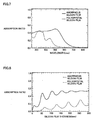
- the wavelength of the laser is not more than 640 nm, the absorption ratio in the amorphous silicon film becomes 10%, or greater. As a result, it becomes easy for the amorphous silicon to absorb the heat from the laser so that the amorphous silicon can be easily polycrystallized.
Landscapes
- Physics & Mathematics (AREA)
- Optics & Photonics (AREA)
- Engineering & Computer Science (AREA)
- Mechanical Engineering (AREA)
- Plasma & Fusion (AREA)
- Chemical & Material Sciences (AREA)
- Materials Engineering (AREA)
- Chemical Kinetics & Catalysis (AREA)
- Thermal Sciences (AREA)
- Metallurgy (AREA)
- Organic Chemistry (AREA)
- Nonlinear Science (AREA)
- Crystallography & Structural Chemistry (AREA)
- General Physics & Mathematics (AREA)
- Recrystallisation Techniques (AREA)
- Thin Film Transistor (AREA)
- Liquid Crystal (AREA)
Abstract
Description
Claims (13)
- A process for a polycrystal silicon film comprising the steps of:forming an amorphous silicon film (33) having a first region (33a) and a second region (33b) that contacts this first region (33a) on a substrate (31);forming a first polycrystal portion (34a) by irradiating the first region (33a) of said amorphous silicon film (33) with a laser (35) of which the wavelength is not less than 390 nm and not more than 640 nm; andforming a second polycrystal portion (34b) that contacts said first polycrystal portion (34a) by irradiating the second region (33b) of said amorphous silicon film (33) and a portion of said first polycrystal portion (34a) that contacts said second region (33b) with said laser (35) of which the wavelength is not less than 390 nm and not more than 640 nm.
- The process for a polycrystal silicon film according to claim 1, wherein said step of forming a first polycrystal portion (34a) includes the formation of said first polycrystal portion (34a) that extends in one direction by scanning the laser (35) on said amorphous silicon film (33) and said step of forming a second polycrystal portion (34b) includes the formation of said second polycrystal portion (34b) that extends along said first polycrystal portion (34a) by scanning said laser (35) in the direction in which said first polycrystal portion (34a) extends.
- The process for a polycrystal silicon film according to claim 1,
wherein said step of forming a first polycrystal portion (34a) includes irradiating said amorphous silicon film (33) with a first laser (35a) of which the wavelength is not less than 390 nm and not more than 640 nm from a first laser light source (120a) and
wherein said step of forming a second polycrystal portion (34b) includes irradiating said amorphous silicon film (33) with a second laser (35b) of which the wavelength is not less than 390 nm and not more than 640 nm from a second laser light source (120b). - The process for a polycrystal silicon film according to claim 1, wherein said laser (35) includes at least one type selected from a group consisting of the second harmonics of an Nd:YAG laser, the second harmonics of an Nd:YVO4 laser, the second harmonics of an Nd:YLF laser, the second harmonics of an Nd:glass laser, the second harmonics of a Yb:YAG laser, the second harmonics of a Yb:glass laser, an Ar ion laser, the second harmonics of a Ti:sapphire laser and a Dye laser.
- The process for a polycrystal silicon film according to claim 3, including a laser irradiation from said second laser light source (120b) after a predetermined period of time has elapsed after a laser irradiation from said first laser light source (120a).
- A production unit for a polycrystal silicon film comprising:an oscillation means (120) for oscillating a laser (35) of which the wavelength is not less than 390 nm and not more than 640 nm;an irradiation means (110) for irradiating an amorphous silicon film (33) formed on a substrate (31) with the laser (35) oscillated from said oscillation means (120);a shifting means (130) for shifting the substrate (31) relative to said irradiation means (110); anda control means (140) for controlling the shifting means (130) to allow the laser (35) to scan said amorphous silicon film (33) so that a first polycrystal portion (34a) is formed by irradiating a portion of said amorphous silicon film (33) with a laser of which the wavelength is not less than 390 nm and not more than 640 nm and so that a second polycrystal portion (34b) that contacts said first polycrystal portion (34a) is formed by irradiating a portion of said amorphous silicon film (33) that overlaps said first polycrystal portion (34a) with said laser (35) of which the wavelength is not less than 390 nm and not more than 640 nm.
- The production unit for a polycrystal silicon film according to claim 6,
wherein said irradiation means includes a first irradiation means (210a) and a second irradiation means (210b);
wherein the amorphous silicon film (33) is irradiated with a portion of the laser oscillated from said oscillation means (420) via said first irradiation means (210a); and
wherein the amorphous silicon film (33) is irradiated with another portion of the laser oscillated from said oscillation means (420) via said second irradiation means (210b). - The production unit for a polycrystal silicon film according to claim 6, wherein the control means (140) controls said first and second irradiation means (210a, 210b), the oscillation means (120) as well as the shifting means (130) so that said second irradiation means (210b) carries out an irradiation by a laser (35b) after a predetermined period of time has elapsed since said first irradiation means (210a) carries out an irradiation by a laser (35a).
- The production unit for a polycrystal silicon film according to claim 6,
wherein said irradiation means includes a first irradiation means (110a) and a second irradiation means (110b) and said oscillation means includes a first oscillation means (120a) and a second oscillation means (120b);
wherein the amorphous silicon film (33) is irradiated with a laser (35a) oscillated from said first oscillation means (120a) via said first irradiation means (110a); and
wherein the amorphous silicon film (33) is irradiated with a laser (35b) oscillated from said second oscillation means (120b) via said second irradiation means (110b). - The production unit for a polycrystal silicon film according to claim 9, wherein the control means (140) controls said first and second irradiation means (110a, 110b), said first and second oscillation means (120a, 120b) as well as the shifting means (130) so that said second irradiation means (110b) carries out an irradiation by a laser (35b) after a predetermined period of time has elapsed since said first irradiation means (110a) carries out an irradiation by a laser (35a).
- The production unit for a polycrystal silicon film according to claim 6, wherein said oscillation means (120) oscillates a laser that includes at least one type selected from a group consisting of the second harmonics of an Nd:YAG laser, the second harmonics of an Nd:YVO4 laser, the second harmonics of an Nd:YLF laser, the second harmonics of an Nd:glass laser, the second harmonics of a Yb:YAG laser, the second harmonics of a Yb:glass laser, an Ar ion laser, the second harmonics of a Ti:sapphire laser and a Dye laser.
- A process for a semiconductor device, comprising the steps of:wherein said step of forming a polycrystal silicon film (34) includes the step of forming a first polycrystal portion (34a) by irradiating the first region (33a) of said amorphous silicon film (33) with a laser (35) of which the wavelength is not less than 390 nm and not more than 640 nm and the step of forming a second polycrystal portion (34b) that contacts said first polycrystal portion (34a) by irradiating the second region (33b) of said amorphous silicon film (33) and a portion of said first polycrystal portion (34a) that contacts said second region (33b) with said laser (35) of which the wavelength is not less than 390 nm and not more than 640 nm.forming an amorphous silicon film (33) having a first region (33a) and a second region (33b) that contacts this first region (33a) on a substrate (31); andforming a polycrystal silicon film (34) by irradiating said amorphous silicon film (33) with a laser (35),
- A semiconductor device wherein a polycrystal silicon film (34) according to claim 12 is used for active regions (39a, 39b).
Applications Claiming Priority (1)
| Application Number | Priority Date | Filing Date | Title |
|---|---|---|---|
| PCT/JP2000/007010 WO2002031871A1 (en) | 2000-10-06 | 2000-10-06 | Method and apparatus for producing polysilicon film, semiconductor device, and method of manufacture thereof |
Publications (3)
| Publication Number | Publication Date |
|---|---|
| EP1256977A1 true EP1256977A1 (en) | 2002-11-13 |
| EP1256977A4 EP1256977A4 (en) | 2008-05-28 |
| EP1256977B1 EP1256977B1 (en) | 2012-02-29 |
Family
ID=11736572
Family Applications (1)
| Application Number | Title | Priority Date | Filing Date |
|---|---|---|---|
| EP00964741A Expired - Lifetime EP1256977B1 (en) | 2000-10-06 | 2000-10-06 | Method and apparatus for producing a polycrystalline silicon film |
Country Status (7)
| Country | Link |
|---|---|
| US (1) | US6884699B1 (en) |
| EP (1) | EP1256977B1 (en) |
| JP (1) | JP4216068B2 (en) |
| KR (1) | KR100473245B1 (en) |
| CN (1) | CN100355026C (en) |
| TW (1) | TW564465B (en) |
| WO (1) | WO2002031871A1 (en) |
Cited By (4)
| Publication number | Priority date | Publication date | Assignee | Title |
|---|---|---|---|---|
| US6717105B1 (en) | 2000-11-02 | 2004-04-06 | Mitsubishi Denki Kabushiki Kaisha | Laser annealing optical system and laser annealing apparatus using the same |
| US7097709B2 (en) | 2002-11-27 | 2006-08-29 | Mitsubishi Denki Kabushiki Kaisha | Laser annealing apparatus |
| US7553778B2 (en) | 2005-02-17 | 2009-06-30 | Mitsubishi Denki Kabushiki Kaisha | Method for producing a semiconductor device including crystallizing an amphorous semiconductor film |
| CN101311344B (en) * | 2008-02-27 | 2010-08-04 | 中国科学院上海光学精密机械研究所 | Preparation and detection device of polysilicon thin film with controllable grain size |
Families Citing this family (29)
| Publication number | Priority date | Publication date | Assignee | Title |
|---|---|---|---|---|
| US6555449B1 (en) | 1996-05-28 | 2003-04-29 | Trustees Of Columbia University In The City Of New York | Methods for producing uniform large-grained and grain boundary location manipulated polycrystalline thin film semiconductors using sequential lateral solidfication |
| JP5244274B2 (en) * | 2000-04-28 | 2013-07-24 | 株式会社半導体エネルギー研究所 | Method for manufacturing semiconductor device |
| US6746942B2 (en) * | 2000-09-05 | 2004-06-08 | Sony Corporation | Semiconductor thin film and method of fabricating semiconductor thin film, apparatus for fabricating single crystal semiconductor thin film, and method of fabricating single crystal thin film, single crystal thin film substrate, and semiconductor device |
| JP4668508B2 (en) * | 2002-05-17 | 2011-04-13 | シャープ株式会社 | Semiconductor crystallization method |
| US6977775B2 (en) * | 2002-05-17 | 2005-12-20 | Sharp Kabushiki Kaisha | Method and apparatus for crystallizing semiconductor with laser beams |
| AU2003272222A1 (en) | 2002-08-19 | 2004-03-03 | The Trustees Of Columbia University In The City Of New York | Process and system for laser crystallization processing of film regions on a substrate to minimize edge areas, and structure of such film regions |
| TWI331803B (en) | 2002-08-19 | 2010-10-11 | Univ Columbia | A single-shot semiconductor processing system and method having various irradiation patterns |
| JP2004128421A (en) * | 2002-10-07 | 2004-04-22 | Semiconductor Energy Lab Co Ltd | Laser irradiation method, laser irradiation apparatus, and manufacturing method of semiconductor device |
| US7332431B2 (en) * | 2002-10-17 | 2008-02-19 | Semiconductor Energy Laboratory Co., Ltd. | Method of manufacturing semiconductor device |
| DE602004020538D1 (en) * | 2003-02-28 | 2009-05-28 | Semiconductor Energy Lab | Method and device for laser irradiation, and method for the production of semiconductors. |
| JP4373115B2 (en) * | 2003-04-04 | 2009-11-25 | 株式会社半導体エネルギー研究所 | Method for manufacturing semiconductor device |
| TWI351713B (en) | 2003-09-16 | 2011-11-01 | Univ Columbia | Method and system for providing a single-scan, con |
| WO2005029551A2 (en) | 2003-09-16 | 2005-03-31 | The Trustees Of Columbia University In The City Of New York | Processes and systems for laser crystallization processing of film regions on a substrate utilizing a line-type beam, and structures of such film regions |
| WO2005029546A2 (en) | 2003-09-16 | 2005-03-31 | The Trustees Of Columbia University In The City Of New York | Method and system for providing a continuous motion sequential lateral solidification for reducing or eliminating artifacts, and a mask for facilitating such artifact reduction/elimination |
| JP2005167084A (en) * | 2003-12-04 | 2005-06-23 | Fujitsu Ltd | Laser crystallization apparatus and laser crystallization method |
| JP4660103B2 (en) * | 2004-03-09 | 2011-03-30 | 三菱電機株式会社 | Laser heat treatment method |
| US7310131B2 (en) * | 2005-08-02 | 2007-12-18 | Asml Netherlands B.V. | Lithographic apparatus and device manufacturing method |
| KR100739631B1 (en) * | 2006-01-16 | 2007-07-16 | 삼성전자주식회사 | Formation method of thin film with single crystal structure |
| KR100740124B1 (en) * | 2006-10-13 | 2007-07-16 | 삼성에스디아이 주식회사 | Polycrystalline Silicon Thin Film Transistor and Manufacturing Method Thereof |
| JP2008211093A (en) * | 2007-02-27 | 2008-09-11 | Sumitomo Heavy Ind Ltd | Laser annealing method or laser annealing device |
| JP2008270540A (en) * | 2007-04-20 | 2008-11-06 | Sony Corp | Semiconductor device manufacturing method and display device |
| WO2008156284A1 (en) * | 2007-06-18 | 2008-12-24 | Cowindst Co., Ltd. | Method of repairing flat pannel display |
| WO2008156286A1 (en) * | 2007-06-18 | 2008-12-24 | Cowindst Co., Ltd. | Method of repairing flat pannel display |
| WO2008156280A1 (en) * | 2007-06-18 | 2008-12-24 | Cowindst Co., Ltd. | Method of repairing flat pannel display |
| US9646831B2 (en) | 2009-11-03 | 2017-05-09 | The Trustees Of Columbia University In The City Of New York | Advanced excimer laser annealing for thin films |
| JP5670862B2 (en) * | 2011-11-02 | 2015-02-18 | トーカロ株式会社 | Method for forming densified layer in thermal spray coating |
| CN104395033B (en) * | 2012-07-04 | 2017-06-23 | 法国圣戈班玻璃厂 | Apparatus and method for laser processing of large area substrates using at least two bridges |
| FR3040319B1 (en) * | 2015-08-25 | 2017-11-24 | Saint Gobain | MODULAR LASER APPARATUS |
| JP7820804B2 (en) * | 2022-03-09 | 2026-02-26 | 株式会社ブイ・テクノロジー | Laser annealing apparatus and laser annealing method |
Family Cites Families (17)
| Publication number | Priority date | Publication date | Assignee | Title |
|---|---|---|---|---|
| US4915772A (en) * | 1986-10-01 | 1990-04-10 | Corning Incorporated | Capping layer for recrystallization process |
| JPH01162376A (en) * | 1987-12-18 | 1989-06-26 | Fujitsu Ltd | Manufacture of semiconductor device |
| US5366926A (en) * | 1993-06-07 | 1994-11-22 | Xerox Corporation | Low temperature process for laser dehydrogenation and crystallization of amorphous silicon |
| JP3195157B2 (en) * | 1994-03-28 | 2001-08-06 | シャープ株式会社 | Semiconductor device manufacturing method and its manufacturing apparatus |
| TW303526B (en) * | 1994-12-27 | 1997-04-21 | Matsushita Electric Industrial Co Ltd | |
| TW305063B (en) * | 1995-02-02 | 1997-05-11 | Handotai Energy Kenkyusho Kk | |
| US6190949B1 (en) * | 1996-05-22 | 2001-02-20 | Sony Corporation | Silicon thin film, group of silicon single crystal grains and formation process thereof, and semiconductor device, flash memory cell and fabrication process thereof |
| DE19825635C1 (en) * | 1998-06-09 | 1999-12-09 | Inst Physikalische Hochtech Ev | Method of producing polycrystalline silicon thin films for microelectronic components, especially thin film transistors on glass substrates |
| KR100430231B1 (en) * | 1998-10-02 | 2004-07-19 | 엘지.필립스 엘시디 주식회사 | Laser Annealing Equipment |
| US6573161B1 (en) * | 1999-03-05 | 2003-06-03 | Seiko Epson Corporation | Thin film semiconductor device fabrication process |
| TW445545B (en) | 1999-03-10 | 2001-07-11 | Mitsubishi Electric Corp | Laser heat treatment method, laser heat treatment apparatus and semiconductor device |
| JP2000260731A (en) * | 1999-03-10 | 2000-09-22 | Mitsubishi Electric Corp | Laser heat treatment method, laser heat treatment apparatus, and semiconductor device |
| JP2000269133A (en) * | 1999-03-16 | 2000-09-29 | Seiko Epson Corp | Method for manufacturing thin film semiconductor device |
| KR100284808B1 (en) * | 1999-03-31 | 2001-03-15 | 구본준 | Method for Crystalline and Activation for a Semiconductor layer Using Laser Annealing |
| JP3562389B2 (en) | 1999-06-25 | 2004-09-08 | 三菱電機株式会社 | Laser heat treatment equipment |
| JP2001023899A (en) * | 1999-07-13 | 2001-01-26 | Hitachi Ltd | Semiconductor thin film, liquid crystal display device using the semiconductor thin film, and method of manufacturing the same |
| US6607971B1 (en) * | 2002-04-30 | 2003-08-19 | Sharp Laboratories Of America, Inc. | Method for extending a laser annealing pulse |
-
2000
- 2000-10-06 CN CNB008167761A patent/CN100355026C/en not_active Expired - Lifetime
- 2000-10-06 US US10/148,562 patent/US6884699B1/en not_active Expired - Lifetime
- 2000-10-06 WO PCT/JP2000/007010 patent/WO2002031871A1/en not_active Ceased
- 2000-10-06 JP JP2002535163A patent/JP4216068B2/en not_active Expired - Lifetime
- 2000-10-06 KR KR10-2002-7007169A patent/KR100473245B1/en not_active Expired - Lifetime
- 2000-10-06 EP EP00964741A patent/EP1256977B1/en not_active Expired - Lifetime
- 2000-10-18 TW TW089121775A patent/TW564465B/en not_active IP Right Cessation
Cited By (4)
| Publication number | Priority date | Publication date | Assignee | Title |
|---|---|---|---|---|
| US6717105B1 (en) | 2000-11-02 | 2004-04-06 | Mitsubishi Denki Kabushiki Kaisha | Laser annealing optical system and laser annealing apparatus using the same |
| US7097709B2 (en) | 2002-11-27 | 2006-08-29 | Mitsubishi Denki Kabushiki Kaisha | Laser annealing apparatus |
| US7553778B2 (en) | 2005-02-17 | 2009-06-30 | Mitsubishi Denki Kabushiki Kaisha | Method for producing a semiconductor device including crystallizing an amphorous semiconductor film |
| CN101311344B (en) * | 2008-02-27 | 2010-08-04 | 中国科学院上海光学精密机械研究所 | Preparation and detection device of polysilicon thin film with controllable grain size |
Also Published As
| Publication number | Publication date |
|---|---|
| EP1256977A4 (en) | 2008-05-28 |
| JPWO2002031871A1 (en) | 2004-02-26 |
| KR100473245B1 (en) | 2005-03-10 |
| CN100355026C (en) | 2007-12-12 |
| KR20020064330A (en) | 2002-08-07 |
| TW564465B (en) | 2003-12-01 |
| WO2002031871A1 (en) | 2002-04-18 |
| EP1256977B1 (en) | 2012-02-29 |
| JP4216068B2 (en) | 2009-01-28 |
| US6884699B1 (en) | 2005-04-26 |
| CN1408122A (en) | 2003-04-02 |
Similar Documents
| Publication | Publication Date | Title |
|---|---|---|
| EP1256977B1 (en) | Method and apparatus for producing a polycrystalline silicon film | |
| US6509212B1 (en) | Method for laser-processing semiconductor device | |
| US6861328B2 (en) | Semiconductor device, manufacturing method therefor, and semiconductor manufacturing apparatus | |
| US6919533B2 (en) | Method for manufacturing a display device including irradiating overlapping regions | |
| US8715412B2 (en) | Laser-irradiated thin films having variable thickness | |
| US7115903B2 (en) | Semiconductor device and semiconductor device producing system | |
| JP4567984B2 (en) | Flat panel display manufacturing equipment | |
| EP1912252A1 (en) | Polysilicon thin film transistor and method of fabricating the same | |
| JPH07249592A (en) | Laser treatment method of semiconductor device | |
| US6723590B1 (en) | Method for laser-processing semiconductor device | |
| US20030148566A1 (en) | Production method for flat panel display | |
| JP4169073B2 (en) | Thin film semiconductor device and method for manufacturing thin film semiconductor device | |
| JP3528577B2 (en) | Semiconductor device manufacturing method and annealing apparatus | |
| JP2006210789A (en) | Method for manufacturing semiconductor crystal thin film, its manufacturing apparatus, photomask and semiconductor device | |
| KR20030082618A (en) | A method for crystallizing of an amorphous Si | |
| JP2001144303A (en) | Active matrix display device and manufacturing method for the same | |
| WO2007108157A1 (en) | Process for producing thin-film transistor, laser crystallization apparatus and semiconductor device | |
| JP2001156296A (en) | Method of driving active matrix display device |
Legal Events
| Date | Code | Title | Description |
|---|---|---|---|
| PUAI | Public reference made under article 153(3) epc to a published international application that has entered the european phase |
Free format text: ORIGINAL CODE: 0009012 |
|
| 17P | Request for examination filed |
Effective date: 20020704 |
|
| AK | Designated contracting states |
Kind code of ref document: A1 Designated state(s): AT BE CH CY DE DK ES FI FR GB GR IE IT LI LU MC NL PT SE |
|
| RBV | Designated contracting states (corrected) |
Designated state(s): AT BE CH CY DE FR GB LI NL |
|
| RAP1 | Party data changed (applicant data changed or rights of an application transferred) |
Owner name: SEIKO EPSON CORPORATION Owner name: MITSUBISHI DENKI KABUSHIKI KAISHA |
|
| A4 | Supplementary search report drawn up and despatched |
Effective date: 20080502 |
|
| RIC1 | Information provided on ipc code assigned before grant |
Ipc: H01L 21/20 20060101AFI20020419BHEP Ipc: C23C 16/24 20060101ALI20080423BHEP Ipc: B23K 26/00 20060101ALI20080423BHEP |
|
| 17Q | First examination report despatched |
Effective date: 20080829 |
|
| REG | Reference to a national code |
Ref country code: DE Ref legal event code: R079 Ref document number: 60046968 Country of ref document: DE Free format text: PREVIOUS MAIN CLASS: H01L0021200000 Ipc: H01L0021020000 |
|
| GRAP | Despatch of communication of intention to grant a patent |
Free format text: ORIGINAL CODE: EPIDOSNIGR1 |
|
| RIC1 | Information provided on ipc code assigned before grant |
Ipc: H01L 21/02 20060101AFI20110722BHEP |
|
| RTI1 | Title (correction) |
Free format text: METHOD AND APPARATUS FOR PRODUCING A POLYCRYSTALLINE SILICON FILM |
|
| RBV | Designated contracting states (corrected) |
Designated state(s): DE FR GB NL |
|
| GRAS | Grant fee paid |
Free format text: ORIGINAL CODE: EPIDOSNIGR3 |
|
| GRAA | (expected) grant |
Free format text: ORIGINAL CODE: 0009210 |
|
| AK | Designated contracting states |
Kind code of ref document: B1 Designated state(s): DE FR GB NL |
|
| REG | Reference to a national code |
Ref country code: GB Ref legal event code: FG4D |
|
| RIN1 | Information on inventor provided before grant (corrected) |
Inventor name: OKAMOTO, TATSUKI,MITSUBISHI DENKI KABUSHIKI K. Inventor name: MIYASAKA, MITSUTOSHI,SEIKO EPSON CORPORATION Inventor name: TOKIOKA, HIDETADA,MITSUBISHI DENKI KABUSHIKI K. Inventor name: OGAWA, TETSUYA,MITSUBISHI DENKI KABUSHIKI KAISHA Inventor name: NISHIMAE, JUNICHI,MITSUBISHI DENKI KABUSHIKI K. Inventor name: SATO, YUKIO,MITSUBISHI DENKI KABUSHIKI KAISHA Inventor name: JIROKU, HIROAKI,SEIKO EPSON CORPORATION Inventor name: INOUE, MITSUO,MITSUBISHI DENKI KABUSHIKI KAISHA |
|
| REG | Reference to a national code |
Ref country code: DE Ref legal event code: R096 Ref document number: 60046968 Country of ref document: DE Effective date: 20120426 |
|
| REG | Reference to a national code |
Ref country code: NL Ref legal event code: T3 |
|
| PLBE | No opposition filed within time limit |
Free format text: ORIGINAL CODE: 0009261 |
|
| STAA | Information on the status of an ep patent application or granted ep patent |
Free format text: STATUS: NO OPPOSITION FILED WITHIN TIME LIMIT |
|
| 26N | No opposition filed |
Effective date: 20121130 |
|
| REG | Reference to a national code |
Ref country code: DE Ref legal event code: R097 Ref document number: 60046968 Country of ref document: DE Effective date: 20121130 |
|
| REG | Reference to a national code |
Ref country code: FR Ref legal event code: PLFP Year of fee payment: 17 |
|
| REG | Reference to a national code |
Ref country code: FR Ref legal event code: PLFP Year of fee payment: 18 |
|
| REG | Reference to a national code |
Ref country code: FR Ref legal event code: PLFP Year of fee payment: 19 |
|
| PGFP | Annual fee paid to national office [announced via postgrant information from national office to epo] |
Ref country code: NL Payment date: 20190912 Year of fee payment: 20 Ref country code: FR Payment date: 20190913 Year of fee payment: 20 |
|
| PGFP | Annual fee paid to national office [announced via postgrant information from national office to epo] |
Ref country code: DE Payment date: 20190924 Year of fee payment: 20 |
|
| PGFP | Annual fee paid to national office [announced via postgrant information from national office to epo] |
Ref country code: GB Payment date: 20191003 Year of fee payment: 20 |
|
| REG | Reference to a national code |
Ref country code: DE Ref legal event code: R071 Ref document number: 60046968 Country of ref document: DE |
|
| REG | Reference to a national code |
Ref country code: NL Ref legal event code: MK Effective date: 20201005 |
|
| REG | Reference to a national code |
Ref country code: GB Ref legal event code: PE20 Expiry date: 20201005 |
|
| PG25 | Lapsed in a contracting state [announced via postgrant information from national office to epo] |
Ref country code: GB Free format text: LAPSE BECAUSE OF EXPIRATION OF PROTECTION Effective date: 20201005 |