EP1256976A2 - Method for producing semiconductor device - Google Patents
Method for producing semiconductor device Download PDFInfo
- Publication number
- EP1256976A2 EP1256976A2 EP02009958A EP02009958A EP1256976A2 EP 1256976 A2 EP1256976 A2 EP 1256976A2 EP 02009958 A EP02009958 A EP 02009958A EP 02009958 A EP02009958 A EP 02009958A EP 1256976 A2 EP1256976 A2 EP 1256976A2
- Authority
- EP
- European Patent Office
- Prior art keywords
- thin film
- semiconductor device
- producing
- dielectric thin
- dielectric
- Prior art date
- Legal status (The legal status is an assumption and is not a legal conclusion. Google has not performed a legal analysis and makes no representation as to the accuracy of the status listed.)
- Withdrawn
Links
Images




Classifications
-
- H—ELECTRICITY
- H10—SEMICONDUCTOR DEVICES; ELECTRIC SOLID-STATE DEVICES NOT OTHERWISE PROVIDED FOR
- H10D—INORGANIC ELECTRIC SEMICONDUCTOR DEVICES
- H10D84/00—Integrated devices formed in or on semiconductor substrates that comprise only semiconducting layers, e.g. on Si wafers or on GaAs-on-Si wafers
- H10D84/80—Integrated devices formed in or on semiconductor substrates that comprise only semiconducting layers, e.g. on Si wafers or on GaAs-on-Si wafers characterised by the integration of at least one component covered by groups H10D12/00 or H10D30/00, e.g. integration of IGFETs
-
- H—ELECTRICITY
- H10—SEMICONDUCTOR DEVICES; ELECTRIC SOLID-STATE DEVICES NOT OTHERWISE PROVIDED FOR
- H10D—INORGANIC ELECTRIC SEMICONDUCTOR DEVICES
- H10D1/00—Resistors, capacitors or inductors
- H10D1/60—Capacitors
- H10D1/68—Capacitors having no potential barriers
- H10D1/682—Capacitors having no potential barriers having dielectrics comprising perovskite structures
-
- H—ELECTRICITY
- H10—SEMICONDUCTOR DEVICES; ELECTRIC SOLID-STATE DEVICES NOT OTHERWISE PROVIDED FOR
- H10P—GENERIC PROCESSES OR APPARATUS FOR THE MANUFACTURE OR TREATMENT OF DEVICES COVERED BY CLASS H10
- H10P14/00—Formation of materials, e.g. in the shape of layers or pillars
- H10P14/60—Formation of materials, e.g. in the shape of layers or pillars of insulating materials
- H10P14/65—Formation of materials, e.g. in the shape of layers or pillars of insulating materials characterised by treatments performed before or after the formation of the materials
- H10P14/6516—Formation of materials, e.g. in the shape of layers or pillars of insulating materials characterised by treatments performed before or after the formation of the materials of treatments performed after formation of the materials
- H10P14/6536—Formation of materials, e.g. in the shape of layers or pillars of insulating materials characterised by treatments performed before or after the formation of the materials of treatments performed after formation of the materials by exposure to radiation, e.g. visible light
- H10P14/6542—Formation of materials, e.g. in the shape of layers or pillars of insulating materials characterised by treatments performed before or after the formation of the materials of treatments performed after formation of the materials by exposure to radiation, e.g. visible light by using coherent radiation, e.g. using a laser
-
- H—ELECTRICITY
- H10—SEMICONDUCTOR DEVICES; ELECTRIC SOLID-STATE DEVICES NOT OTHERWISE PROVIDED FOR
- H10P—GENERIC PROCESSES OR APPARATUS FOR THE MANUFACTURE OR TREATMENT OF DEVICES COVERED BY CLASS H10
- H10P14/00—Formation of materials, e.g. in the shape of layers or pillars
- H10P14/60—Formation of materials, e.g. in the shape of layers or pillars of insulating materials
- H10P14/65—Formation of materials, e.g. in the shape of layers or pillars of insulating materials characterised by treatments performed before or after the formation of the materials
- H10P14/6516—Formation of materials, e.g. in the shape of layers or pillars of insulating materials characterised by treatments performed before or after the formation of the materials of treatments performed after formation of the materials
- H10P14/6544—Formation of materials, e.g. in the shape of layers or pillars of insulating materials characterised by treatments performed before or after the formation of the materials of treatments performed after formation of the materials to change the morphology of the insulating materials, e.g. transformation of an amorphous layer into a crystalline layer
-
- H—ELECTRICITY
- H10—SEMICONDUCTOR DEVICES; ELECTRIC SOLID-STATE DEVICES NOT OTHERWISE PROVIDED FOR
- H10P—GENERIC PROCESSES OR APPARATUS FOR THE MANUFACTURE OR TREATMENT OF DEVICES COVERED BY CLASS H10
- H10P14/00—Formation of materials, e.g. in the shape of layers or pillars
- H10P14/60—Formation of materials, e.g. in the shape of layers or pillars of insulating materials
- H10P14/69—Inorganic materials
- H10P14/692—Inorganic materials composed of oxides, glassy oxides or oxide-based glasses
- H10P14/6938—Inorganic materials composed of oxides, glassy oxides or oxide-based glasses the material containing at least one metal element, e.g. metal oxides, metal oxynitrides or metal oxycarbides
- H10P14/69398—Inorganic materials composed of oxides, glassy oxides or oxide-based glasses the material containing at least one metal element, e.g. metal oxides, metal oxynitrides or metal oxycarbides the material having a perovskite structure, e.g. BaTiO3
-
- H—ELECTRICITY
- H10—SEMICONDUCTOR DEVICES; ELECTRIC SOLID-STATE DEVICES NOT OTHERWISE PROVIDED FOR
- H10P—GENERIC PROCESSES OR APPARATUS FOR THE MANUFACTURE OR TREATMENT OF DEVICES COVERED BY CLASS H10
- H10P95/00—Generic processes or apparatus for manufacture or treatments not covered by the other groups of this subclass
- H10P95/06—Planarisation of inorganic insulating materials
Definitions
- This invention relates to a method for producing a semiconductor device having a dielectric capacitor. More particularly, it relates to a method for producing a semiconductor device that can operate at a low supply voltage.
- ferroelectric memory or the DRAM there is provided a switching transistor and information is stored in a capacitor which is connected to one diffusion layer of the switching transistor and composes a memory cell.
- a ferroelectric capacitor provided in a ferroelectric memory in which a ferroelectric thin film, such as PZT (PbZr x Ti 1-x O 3 ), PLZT (Pb 1- y La y Zr x Ti 1-x O 3 ), SBT (SrBi 2 Ta 2 O 9 ) or the like, is used as a capacitor insulating film, is capable of storing the non-volatile information based on polarization of the ferroelectric material.
- a ferroelectric thin film such as PZT (PbZr x Ti 1-x O 3 ), PLZT (Pb 1- y La y Zr x Ti 1-x O 3 ), SBT (SrBi 2 Ta 2 O 9 ) or the like, is used as a capacitor insulating film, is capable of storing the non-volatile information based on polarization of the ferroelectric material.
- a high dielectric constant capacitor provided in a DRAM in which a high dielectric constant thin film, such as BST (Ba x Sr 1-x Ti o ) or the like, is used as a capacitor insulating film, can be reduced in effective film thickness with increase in capacity.
- a high dielectric constant thin film such as BST (Ba x Sr 1-x Ti o ) or the like
- a conventional ferroelectric memory includes a ferroelectric capacitor, which is made up of a lower electrode 13, a ferroelectric thin film 14 and an upper electrode 15, formed in this order, as shown in Fig. 10, above a switching transistor (not shown), via inter-layer insulating film(not shown).
- the lower electrode is connected to one of the diffusion layers of the switching transistor via a plug filled into the contact hole which is formed in the inter-layer insulating film.
- the ferroelectric thin film is formed on the lower electrode by a film-deposition method, such as a sputtering method, a sol/gel method or a CVD method, and is made to have the perovskite crystal structure on annealing at a preset temperature.
- the dielectric thin film, thus formed has a polycrystalline structure and there is roughness present on the thin film surface.
- the thickness of the ferroelectric thin film For maintaining a capacitor in keeping pace with miniaturization and high density of the memory cell, it is meritorious to reduce the thickness of the ferroelectric thin film.
- an optimum ferroelectric characteristic such as a polarization inversion characteristic
- the crystal grain size be not less than approximately 50 nm, and hence there inevitably exist surface roughness of a size close to the crystal grain size on the surface of the ferroelectric thin film. Consequently, there is raised a problem that, if the film thickness is reduced, the concentration of electric filed (leakage current) tends to be produced in a film thickness thin portion in the recess in the film surface.
- This concentration of the electric field deteriorates insulating properties of the ferroelectric thin film or the polarization inversion characteristic and hence obstructs reduction in film thickness of the ferroelectric film to render the realization of the low voltage operation impossible.
- planarization of the roughness on the ferroelectric thin film surface for the realization of the low voltage operation.
- this planarization is to be achieved by re-flow processing, this approach is not desirable because there is some possibility that an electrode or metal wiring located below the thin film tend to be damaged by high temperature in the re-flow processing.
- JP Patent Kokai JP-A-2000-81642 there has been disclosed a technology in which a hydrogen-containing amorphous semiconductor film is irradiated with a laser a plural number of times to form a crystalline semiconductor presenting surface roughness to a lesser extent and also having larger crystal grain size. That is, the laser irradiation is carried out in order to convert the amorphous silicon to polycrystalline silicon.
- this technology may suffice for silicon, it cannot be applied for the case with the ferroelectric material of the perovskite structure.
- Another object of the present invention is to provide a method for producing a semiconductor device employing a dielectric capacitor which realizes the low voltage operation.
- a further object of the present invention is to provide a method for producing a dielectric capacitor which doe not damage metal wiring layer and the like.
- a further object of the present invention of the present invention is to provide a method for producing a semiconductor device employing the dielectric capacitor having a satisfactory transistor characteristic.
- a method for producing a semiconductor device having a dielectric capacitor comprising: a first step of forming a lower electrode(13); a second step of forming a polycrystalline dielectric thin film (14) having roughness on its surface on the lower electrode; a third step of rapidly heating a surface layer portion of a predetermined film thickness in the dielectric thin film to melting and quenching the portion to flatten out the surface of the thin film; and a fourth step of forming an upper electrode(15) on the dielectric thin film.
- the maximum height of the surface roughness of the dielectric thin film, formed in the second step is preferably not less than 50 nm. It is because a capacitor may then be formed in which the dielectric thin film has a crystal grain size not larger than 50 nm and which exhibits an optimum polarization hysteresis characteristic.
- the thickness to the apex of the maximum projection from the bottom surface of the lower electrode of the dielectric thin film formed by the second step is preferably not less than 200 nm, because the crystal grain size of a constant value can then be maintained even after flattening out processing.
- the aspect ratio of crystal grains of the dielectric thin film, formed by the above-described second step is preferably not larger than 200 nm, because this guarantees a certain constant crystal grain size even after flattening processing.
- a method for producing a semiconductor device having a dielectric capacitor comprising: a first step of forming a lower electrode; a second step of forming, on the lower electrode, a polycrystalline dielectric thin film containing crystals of a preset grain size; a third step of forming a processed film obtained on amorphizing or crystallizing a surface layer portion of a preset film thickness in the dielectric thin film, in such a manner as to maintain the crystal grain size of a lower surface portion thereof at such a value as to retain a desired characteristic of the dielectric material; and a fourth step of forming an upper electrode on the dielectric thin film. It is because crystallization or amorphizing of the crystals is thought to be among the characteristics proper to the dielectric material of he perovskite crystal structure.
- the desired characteristic of the dielectric is a polarization hysteresis characteristic.
- a fifth step of etching the surface layer portion, rapidly heated and subsequently quenched, or amorphized, or crystallized, to a flat surface is preferably provided between the third and fourth steps. It is because this demonstrates desirable properties inherently owned by a dielectric material.
- a sixth step of annealing the surface layer portion of the as-etched dielectric thin film is preferably provided because this repairs damages done on etching to the dielectric thin film surface.
- a plane surface on the polycrystalline dielectric thin film is preferably exposed by the above fifth step because this demonstrates optimum properties inherently owned by the dielectric material.
- the dielectric thin film in the second step preferably has a crystal grain size not less than 50 nm because this achieves optimum dielectric characteristics.
- the dielectric thin film in the second step is preferably formed at a temperature not higher than 500°C by chemical vapor deposition because this does not damage e.g., the metal wiring layers.
- the third and sixth steps are desirably carried out by irradiating the dielectric thin film with excimer laser, which excimer laser is preferably XeCl excimer laser. It is because this makes amorphous or crystallize the surface layer portion to a grain size smaller than the crystal grain size, with a preset film thickness, as well as to planarize the surface.
- the energy density of the excimer laser in the aforementioned sixth step is desirably lower than that in the third step.
- the energy density of the excimer laser in the aforementioned third step is desirably 160 to 200 mJ/cm 2
- that in the aforementioned sixth step is desirably 140 to 160 mJ/cm 2 . It is because this flattens the thin film surface and suppresses the film thickness of the polycrystalline or amorphous layer of a small grain size while lessening the deterioration of polarization hysteresis characteristics.
- the dielectric thin film is preferably formed of a dielectric material of the perovskite crystal structure, more preferably a ferroelectric material or a high dielectric constant material, and most preferably PZT.
- the etching is preferably plasma etching because it is superior in its machining accuracy.
- a step of selectively forming at least one metal wiring layer is preferably provided before forming the dielectric capacitor. It is because no damage is done to the metal wiring even if the metal wiring is formed below the capacitor according to the present invention.
- a method for producing the semiconductor device includes, the following steps,
- the dielectric thin film surface is planarized to prevent leak current and is made possible to demonstrate various characteristics proper to the dielectric material, such as a polarization hysteresis characteristic.
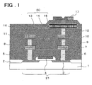
- Fig. 1 is a partial schematic cross-sectional view of the structure of a semiconductor device according to a first embodiment of the present invention.
- Fig.2 is a partial circuit diagram of a semiconductor device according to the first embodiment of the present invention.
- a memory cell 22 includes a switching transistor 21 and a dielectric capacitor 20.
- a switching transistor 21 has a gate connected to a word line 23, while having one of a source and a drain connected to a bit line 25 and having the other of the source and the drain connected via a capacitor 20 to a plate line 24.
- this semiconductor device includes an MOS type switching transistor 21 on a silicon substrate 1, while including a dielectric capacitor 20 on the switching transistor 21 via inter-layer insulating films 5, 8 and 11.
- the first metal wirings 7 are electrically connected through a pair of plugs 6 to a diffusion layer 3 of the switching transistor.
- One of the first metal wirings 7 is used as a wiring interconnecting the dielectric capacitor 20 and the switching transistor 21, while the other first wiring 7 is used as a bit line 25 of Fig.2.
- first vias 9, formed e.g., of tungsten are electrically connected through a second via 9 to a lower electrode 13.
- a multi-layer metal wiring structure comprised of the first metal wirings 7 and the second metal wirings 10.
- the dielectric capacitor 20 is made up by the lower electrode 13, a thin dielectric film 14 and an upper electrode 15, in this order.
- the lower electrode 13 and the diffusion layer 3 are electrically interconnected through the plug 6, a first metal wiring 7, a first via 9, a second metal wiring 10 and a second via 12.
- metals weaker in affinity with oxygen such as Pt, Pd, Ir, Rh, Ir, Rh, Os, Au, Ag, Ru, and the like or electrically conductive oxide films such as PtO x , PdO x , IrO x , RhO x , OsO x , AuO x , AgO x , RuO x , and the like are used, in order to prevent deterioration of spontaneous polarization of a ferroelectric material due to oxygen deficiency.
- barrier layer formed of an electrically conductive nitride film, such as TiN, between the lower electrode 13 and the second via 12, in order to prevent inter-reaction and inter-diffusion between Pt of the lower electrode 13 and tungsten of the second via 12.
- the dielectric thin film 14 is made up of a ferroelectric thin film such as BaTiO 3 , PbTiO 3 , PZT, PLZT, SBT and the like, or of a high-dielectric constant material, such as BST and the like.
- a fourth inter-layer insulating film 16 On the dielectric capacitor 20 is formed a fourth inter-layer insulating film 16 and a third metal wiring 17 is selectively formed within and over a contact hole provided in the fourth inter-layer insulating film 16.
- a third metal wiring 17 is used as a plate wiring 24 in Fig.2.
- the structure of the memory cell 22 of the first embodiment lying below the lower electrode 13 is the same as the LSI not having a capacitor. Consequently, the structure can be prepared by a routine production process same as production process of a pre-existing logic circuit.
- Figs. 3A to 3E and Figs. 4E and 4F are cross-sectional views schematically showing the manufacture process of the semiconductor device according to the first embodiment of the present invention.
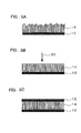
- Figs. 5A to 5C are cross-sectional views schematically showing the manufacture process of the dielectric capacitor according to the first embodiment of the present invention.
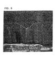
- Fig.6 is a photo, taken by an electron microscope, of the cross-section of an as-formed dielectric thin film of a semiconductor device according to the first embodiment of the present invention
- Fig. 7 is a photo, taken by an electron microscope, of the dielectric thin film of the semiconductor device of the first embodiment of the present invention, following laser irradiation,
- an MOS transistor such as a memory cell unit or a logic circuit unit, is formed on a silicon substrate 1, by a routine LSI manufacture process, as shown in Fig. 3A. That is, an oxide film 2 is selectively formed to delimit a device forming area by this oxide film 2. A gate electrode 4 and the diffusion layer 3 are then formed. The first inter-layer insulating film 5 then is formed on the silicon substrate 1. The so formed first inter-layer insulating film 5 is planarized by the CMP method or by a re-flow method.
- the first metal wirings 7 and the plugs 6 interconnecting the first metal wirings 7 and the diffusion layers 3 then are formed.
- the forming method there are a method consisting in forming the plugs 6 by tungsten plugs and subsequently depositing and processing the first metal wirings 7, and a dualdamasin method consisting in processing the first inter-layer insulating films 5 to the shape of the plugs 6 and the first metal wirings 7, burring a metal, then removing excess metal to form the plugs 6 and the first metal wirings 7 simultaneously.
- the plugs 6 are bored by etching, and the barrier metal, such as Ti or TiN, is then formed by contact injection and activation. Tungsten is then formed on the entire wafer surface by the CVD method. Then, surface tungsten is removed by the CMP method or an etch back to form tungsten plugs. The tungsten plugs my also be formed by selective growth of tungsten.
- the first metal wirings 7 then are selectively formed on the plug
- the first metal wirings 7 are formed by a composite layer, made up by a barrier metal, such as Ti or TiN, an alloy layer, mainly composed of Al or Cu, and an anti-reflection film of, for example, TiN, and are deposited as by a sputtering method or a CVD method followed by etching.
- a barrier metal such as Ti or TiN
- an alloy layer mainly composed of Al or Cu
- the second inter-layer insulating film 8 is formed and after planarization of the film 8, a pair of first vias 9 and second metal wirings 10 are then formed on the first metal wirings 7.
- the first vias 9 and the second metal wirings 10 are formed by a method similar to that for the plugs 6 and the first metal wirings 7.
- a third inter-layer insulating film 11 then is formed, as shown in Fig.3D, and a second via 12 is formed e.g., with a tungsten plug on the second metal wirings 10, as in the case of the plug 6.
- surface tungsten is preferably removed by a CMP method. It is because the dielectric capacitor may then be subsequently formed on a completely planarized surface.
- Annealing is then carried out in a hydrogen-containing atmosphere.
- the annealing temperature is preferably not lower than 300°C and not higher than 500°C. The reason is that the annealing temperature not higher than 300°C has only poor effect in improving transistor characteristics, while the annealing temperature not lower than 500°C tends to break the metal wirings 7, and 10.
- a dielectric capacitor then is formed on the third inter-layer insulating film 11 for connection to the second via 12.
- the dielectric capacitor is formed by the following processes.
- the lower electrode 13 formed of a noble metal, such as Pt, Ir, Ru or the like, or an electrically conductive oxide, such as IrO 2 , RuO 2 or the like, is formed on the third inter-layer insulating film 11, by a sputtering method or the like.
- a noble metal such as Pt, Ir, Ru or the like
- an electrically conductive oxide such as IrO 2 , RuO 2 or the like
- a barrier film formed of, for example, TiN, is formed below the layer of this noble metal or the electrically conductive oxide, in order to prevent inter-reaction and inter-diffusion between tungsten of the second via 12 and Pt of the lower electrode 13.
- the dielectric thin film 14 made up of such as Pb(Zr, Ti)O 3 (PZT), (Ba, Sr)TiO 3 (BST), SrTiO 3 (ST) or the like is formed on the lower electrode 13, by a CVD method or the like.
- the thin PZT film In forming the thin PZT film, heating at a temperature exceeding 600°C is required in order to obtain optimum PZT thin films by a routine sol/gel method or by a sputtering method. Such high temperature tends to cause breaking of the metal wiring or a high electrical resistance and hence is not applicable to the present structure. It is therefore desirable to perform film deposition at a lower temperature of the order of 450°C, as in the CVD method.
- the PZT thin film of a satisfactory crystal state, with the crystal grain size of the order of 50 nm or larger, may be formed by the CVD method in a temperature range of from 350°C to 500°C.
- the ST thin film may be formed at 450°C by the ECR-CVD method, as discussed in, for example, International Electron Devices Meeting Technical Digest) 1994, pp.831.
- the thickness of the PZT film from the bottom surface of the lower electrode to the apex of the maximum projection is preferably not less than 200 nm. That is, the sum of 50 nm which is the necessary smallest possible grain size of PZT, the depth of 100 nm affected by the energy of the XeCl excimer laser energy which acts on the PZT, and the maximum height of the surface roughness of 50 nm, is 200 nm.
- the photo taken by an electron microscope of the cross-section of the PZT thin film is shown in Fig.6.
- the maximum height R max according to JIS B 0601 distance from the bottom of the maximum recess to the apex of the maximum projection of the surface roughness of the PZT thin film is not less than 50 nm, with the projection being of an edge shape.
- the PZT crystal grain is a columnar crystal with the aspect ratio not less than 2.5. The pronounced surface roughness is produced on crystal grain growth to not less than 50 nm sufficient to display the polarization hysteresis characteristic of PZT.
- the upper electrode is formed as the PZT thin film surface presents this kind of surface roughness, the distance between the upper and lower electrodes is decreased in the recessed part so that electric field concentration tends to be produced to lower the insulating properties or to deteriorate a polarization inversion characteristic. For this reason, the planarization process of the surface of the dielectric thin film as described below is performed.
- the depth to which the energy reaches is meritoriously constant and is on the order of 100 nm from the surface.
- the result is that the surface layer portion in which the crystal is of the micro-crystal size or which has been amorphized may be formed to an approximately uniform film thickness.
- the energy density of the XeCl excimer laser where the surface of the PZT thin film 14 commences to be dissolved is 160 to 200 mJ/cm 2 as measured in atmosphere or under a reduced pressure.
- Fig.7 The photo of the cross-section of the PZT thin film, taken with an electron microscope, is shown in Fig.7, from which it may be seen that the film surface has been planarized to such an extent that the pre-irradiation surface shown in Fig.6 is only a poor comparison.
- the depth the energy reaches in the case of the KrF excimer laser is on the order of 50 m from the surface.
- the upper electrode 15 is formed by a method similar to the method as used for the lower electrode 13.
- the lower electrode 13, the dielectric thin film 14 and the upper electrode 15 are processed by etching.
- the dielectric capacitor as shown in Fig.4E is completed.
- a fourth inter-layer insulating film 16 is then formed on the third inter-layer insulating film 11 and on the dielectric capacitor and a contact hole then is formed in an upper portion of the capacitor. Then, as shown in Fig. 4(F), a third metal wiring 17, which serves as a plate line, is formed similarly to the first and second metal wirings 7 and 10.
- the third metal wiring 17 is used only as the plate line 24, while it is not used in other logic circuits. Consequently, there is no device change in the logic circuit unit caused by forming a memory cell array unit employing the dielectric capacitor.
- a passivation film not shown, formed of, for example, SiON.
- FIGS. 8A to 8D are schematic cross-sectional views showing the method for producing a dielectric capacitor of a semiconductor device according to the second embodiment of the present invention.
- a PZT thin film 14 is formed by the CVD method on the lower electrode 13 as in the first embodiment, and an excimer laser 30 is applied on the surface of the PZT thin film 14 as in the first embodiment, the vicinity of the thin film affected by laser irradiation (to a depth of approximately 10 nm) is turned into a
- etching gases HBr/Ar/CF 4 is used, with the flow velocity being 20/8/30 sccm, with the gas pressure being 0.532 Pa (4mTorr), an etching rate being 2 nm/sec. So, the thickness of approximately 50 nm is etched in 25 sec.
- the dielectric capacitor to demonstrate a polarization hysteresis characteristic proper to PZT.
- the PZT thin film surface may be slightly damaged by the etching, the maximum height of surface roughness of the thin film at this time is a few nm, thus being smaller than undulations on the thin film surface prior to the laser irradiation, which are approximately 70 nm, so that electric field concentration is advantageously less liable to occur than with a thin film not subjected to laser illumination.
- the dielectric thin film inherently has outstanding surface roughness such that it is not planarized significantly.
- the upper electrode 15 may be formed on the PZT thin film, as in the first embodiment.
- FIGS. 9A to 9E are schematic cross-sectional views showing a method for producing a dielectric capacitor of a semiconductor device of the third embodiment of the present invention.
- the surface of the PZT thin film 14 is irradiated with the excimer laser 30 as indicated in the first embodiment, and the polycrystalline to amorphous portion of the small crystal grain size on the surface layer portion of the PZT thin film 14 is plasma-etched 31, as indicated in the second embodiment, it may be an occurrence that the thin film surface is damaged to produce defects, which in turn may cause electric field concentration. It is therefore preferable to anneal the damaged portion by further irradiation of an excimer laser 32. This annealing eliminates defects present on the PZT thin film surface to provide a planarized surface to evade the electric field concentration.
- the size of the undulations (see Fig.9C) caused on the PZT film surface by the etching is smaller than the undulations (see Fig.9A) on the PZT thin film prior to the first irradiation of the excimer laser 30, it is possible to realize a film thickness smaller than the film thickness of the surface layer portion of the PZT thin film micro-crystallized or amorphized by the irradiation of the first excimer laser 30.
- a dielectric thin film, having a surface planarized is produced, so that electric field concentration is prohibited to contribute to the miniaturization and high density of the memory cell.
- ferroelectric capacitor capable of performing a low voltage operation can be produced.
- the main usage of this ferroelectric capacitor is the ferroelectric memory for low voltage operation, a low voltage operation (from 3V to 2.5V and thence to 1.8V) may be realized in other deices exploiting a ferromagnetic material.
- the electric field concentration may be eliminated by planarizing surface roughness innate to the polycrystalline film by laser processing.
- the dielectric thin film is formed and surface processing is achieved at a lower temperature, it is possible to provide a high quality product not having damages in its metal layer.
Landscapes
- Semiconductor Memories (AREA)
- Semiconductor Integrated Circuits (AREA)
- Ceramic Capacitors (AREA)
Abstract
Description
Fig.6 is a photo, taken by an electron microscope, of the cross-section of an as-formed dielectric thin film of a semiconductor device according to the first embodiment of the present invention, Fig. 7 is a photo, taken by an electron microscope, of the dielectric thin film of the semiconductor device of the first embodiment of the present invention, following laser irradiation,
Claims (21)
- A method for producing a semiconductor device having at least a dielectric capacitor, said method comprising:a first step of forming a lower electrode;a second step of forming a polycrystalline dielectric thin film on said lower electrode, said polycrystalline dielectric thin film having surface roughness;a third step of heating rapidly a surface layer portion of said dielectric thin film of a predetermined film thickness to melting and quenching said portion to planarize the surface of said thin film; anda fourth step of forming an upper electrode on said dielectric thin film.
- The method for producing the semiconductor device as defined in claim 1, characterized in that the maximum height of surface roughness of the dielectric thin film formed by said second step is not less than 50 nm.
- The method for producing the semiconductor device as defined in claim 1, characterized in that the thickness of the dielectric thin film formed by said second step as from a bottom surface facing towards the lower electrode to an apex of the maximum projection is not less than 200 nm.
- The method for producing the semiconductor device as defined in claim 1, characterized in that an aspect ratio of a crystal grain of the dielectric thin film formed by said second step is not less than, 2.5.
- A method for producing a semiconductor device having at least a dielectric capacitor, said method comprising:a first step of forming a lower electrode;a second step of forming, on said lower electrode, a polycrystalline dielectric thin film containing crystals of a preset grain size;a third step of forming a processed film obtained on amorphizing or micro-crystallizing a surface layer portion of a preset film thickness of said dielectric thin film, in such a manner as to maintain the crystal grain size of a lower surface portion of said surface layer portion in said dielectric thin film at such a value as to retain a desired characteristic of the dielectric material; anda fourth step of forming an upper electrode on said dielectric thin film.
- The method for producing a semiconductor device as defined in claim 5, characterized in that the desired characteristic of said dielectric material is a polarization hysteresis characteristic.
- The method for producing a semiconductor device as defined in any one of claims 1 to 6, characterized in that said method further comprisesa fifth step intermediate between said third and fourth steps, said fifth step being a step of etching said surface layer portion, rapidly heated and quenched, or amorphized or micro-crystallized, to a planar state.
- The method for producing a semiconductor device as defined in claim 7, characterized in that said method further comprisessixth step being a step of annealing the surface layer portion of the as-etched dielectric thin film.a sixth step intermediate between said fifth and fourth steps, said
- The method for producing a semiconductor device as defined in claim 7 or 8, characterized in that the planar surface of the polycrystalline dielectric thin film is exposed by said fifth step.
- The method for producing a semiconductor device as defined in any one of claims 1 to 9, characterized in that the dielectric thin film in said fourth step includes at least a crystal of crystal grain size not less than 50 nm.
- The method for producing a semiconductor device as defined in any one of claims 1 to 10, characterized in that the dielectric thin film in said second step is formed at a temperature not higher than 500°C by chemical vapor deposition.
- The method for producing a semiconductor device as defined in any one of claims 1 to 11, characterized in that said third and sixth steps are carried out as an excimer laser is applied on said dielectric thin film surface.
- The method for producing a semiconductor device as defined in claim 12, characterized in that the excimer laser is a XeCl excimer laser.
- The method for producing a semiconductor device as defined in claim 12 or 13, characterized in that the energy density of the excimer laser in said sixth step is lower than that in said third step.
- The method for producing a semiconductor device as defined in any one of claims 12 to 14, characterized in that the energy density of the excimer laser in said third step is 160 to 200 mJ/cm2.
- The method for producing a semiconductor device as defined in any one of claims 12 to 15, characterized in that the energy density of the excimer laser in said sixth step is 140 to 160 mJ/cm2.
- The method for producing a semiconductor device as defined in any one of claims 1 to 16, characterized in that said dielectric thin film formed in said second step is made up of a dielectric material of a perovskite crystal structure.
- The method for producing a semiconductor device as defined in any one of claims 1 to 17, characterized in that said dielectric thin film formed in said second step is made up of a ferroelectric material or a high dielectric constant material.
- The method for producing a semiconductor device as defined in any one of claims 7 to 18, characterized in that said etching is a plasma etching.
- The method for producing a semiconductor device as defined in any one of claims 1 to 19, characterized in that said method further comprises a step of selectively forming at least a first layer metal wiring prior to forming said dielectric capacitor.
- The method for producing a semiconductor device as defined in any one of claims 1 to 9, characterized in that in the second step, the surface roughness on crystal grain growth in of said polycrystalline dielectric thin film is of a value not less than a predetermined size sufficient to display a polarization hysteresis characteristic of said dielectric thin film.
Applications Claiming Priority (2)
| Application Number | Priority Date | Filing Date | Title |
|---|---|---|---|
| JP2001137456A JP4626925B2 (en) | 2001-05-08 | 2001-05-08 | Manufacturing method of semiconductor device |
| JP2001137456 | 2001-05-08 |
Publications (2)
| Publication Number | Publication Date |
|---|---|
| EP1256976A2 true EP1256976A2 (en) | 2002-11-13 |
| EP1256976A3 EP1256976A3 (en) | 2004-11-10 |
Family
ID=18984561
Family Applications (1)
| Application Number | Title | Priority Date | Filing Date |
|---|---|---|---|
| EP02009958A Withdrawn EP1256976A3 (en) | 2001-05-08 | 2002-05-03 | Method for producing semiconductor device |
Country Status (6)
| Country | Link |
|---|---|
| US (1) | US20020168831A1 (en) |
| EP (1) | EP1256976A3 (en) |
| JP (1) | JP4626925B2 (en) |
| KR (1) | KR20020085843A (en) |
| CN (1) | CN1384541A (en) |
| TW (1) | TW541688B (en) |
Families Citing this family (11)
| Publication number | Priority date | Publication date | Assignee | Title |
|---|---|---|---|---|
| US6916722B2 (en) * | 2002-12-02 | 2005-07-12 | Taiwan Semiconductor Manufacturing Co., Ltd. | Method to fabricate high reliable metal capacitor within copper back-end process |
| US7251346B2 (en) | 2002-11-19 | 2007-07-31 | Honda Motor Co., Ltd. | Moving object detection device, moving object detection method, and moving object detection program |
| US6955997B1 (en) * | 2003-05-16 | 2005-10-18 | Advanced Micro Devices, Inc. | Laser thermal annealing method for forming semiconductor low-k dielectric layer |
| JP3910209B2 (en) * | 2004-03-05 | 2007-04-25 | 松下電器産業株式会社 | Piezoelectric element, inkjet head, angular velocity sensor, manufacturing method thereof, and inkjet recording apparatus |
| JP2005340424A (en) * | 2004-05-26 | 2005-12-08 | Nec Electronics Corp | Semiconductor device and method for manufacturing the same |
| JP4904671B2 (en) | 2004-06-24 | 2012-03-28 | 日本電気株式会社 | SEMICONDUCTOR DEVICE, ITS MANUFACTURING METHOD, AND ELECTRONIC DEVICE |
| JP2006190809A (en) | 2005-01-06 | 2006-07-20 | Fujitsu Ltd | Manufacturing method of semiconductor device |
| KR101035611B1 (en) * | 2008-06-18 | 2011-05-19 | 주식회사 동부하이텍 | MOS transistor and its manufacturing method |
| KR101303853B1 (en) * | 2011-02-01 | 2013-09-04 | 한국과학기술연구원 | Method for formation ferroelectrics thin film and method for manufacturing device of planar structure |
| JP5561300B2 (en) * | 2012-03-26 | 2014-07-30 | 富士通セミコンダクター株式会社 | Manufacturing method of semiconductor device |
| JP2016072502A (en) * | 2014-09-30 | 2016-05-09 | 富士通セミコンダクター株式会社 | Semiconductor device and manufacturing method thereof |
Family Cites Families (11)
| Publication number | Priority date | Publication date | Assignee | Title |
|---|---|---|---|---|
| US5310990A (en) * | 1991-06-03 | 1994-05-10 | The United Stated Of America As Represented By The Secretary Of The Navy | Method of laser processing ferroelectric materials |
| JP3206105B2 (en) * | 1992-06-09 | 2001-09-04 | セイコーエプソン株式会社 | Method for manufacturing dielectric element and semiconductor memory device |
| JP3683972B2 (en) * | 1995-03-22 | 2005-08-17 | 三菱電機株式会社 | Semiconductor device |
| JP2000223666A (en) * | 1999-01-28 | 2000-08-11 | Sharp Corp | Method for manufacturing semiconductor memory device |
| JP2000031411A (en) * | 1998-07-09 | 2000-01-28 | Oki Electric Ind Co Ltd | Manufacturing method of ferroelectric thin film |
| JP3489093B2 (en) * | 1998-12-02 | 2004-01-19 | 富士通株式会社 | Method for manufacturing polycrystalline insulating film |
| KR100308190B1 (en) * | 1999-01-20 | 2001-09-26 | 윤종용 | Method of removing pyrochlore caused during a ferroelectric crystalline dielectric film process |
| JP2002164514A (en) * | 2000-11-24 | 2002-06-07 | Nec Corp | Method for manufacturing semiconductor device |
| JP2002280380A (en) * | 2001-03-19 | 2002-09-27 | Japan Science & Technology Corp | Semiconductor device film forming method |
| JP2002314045A (en) * | 2001-04-11 | 2002-10-25 | Seiko Epson Corp | Method of forming ferroelectric thin film, ferroelectric memory, and method of manufacturing ferroelectric memory |
| JP2002329844A (en) * | 2001-05-01 | 2002-11-15 | Hitachi Ltd | Thin film multilayer wiring circuit board and method of manufacturing the same |
-
2001
- 2001-05-08 JP JP2001137456A patent/JP4626925B2/en not_active Expired - Fee Related
-
2002
- 2002-04-29 US US10/135,026 patent/US20020168831A1/en not_active Abandoned
- 2002-05-03 EP EP02009958A patent/EP1256976A3/en not_active Withdrawn
- 2002-05-07 KR KR1020020025120A patent/KR20020085843A/en not_active Ceased
- 2002-05-07 TW TW091109537A patent/TW541688B/en active
- 2002-05-08 CN CN02119113A patent/CN1384541A/en active Pending
Also Published As
| Publication number | Publication date |
|---|---|
| JP4626925B2 (en) | 2011-02-09 |
| EP1256976A3 (en) | 2004-11-10 |
| KR20020085843A (en) | 2002-11-16 |
| TW541688B (en) | 2003-07-11 |
| JP2002334970A (en) | 2002-11-22 |
| CN1384541A (en) | 2002-12-11 |
| US20020168831A1 (en) | 2002-11-14 |
Similar Documents
| Publication | Publication Date | Title |
|---|---|---|
| US7927889B2 (en) | Method for manufacturing ferroelectric memory device and ferroelectric memory device | |
| US6635497B2 (en) | Methods of preventing reduction of IrOx during PZT formation by metalorganic chemical vapor deposition or other processing | |
| EP0860868A2 (en) | Method for treating a dielectric used in semiconductor devices and DRAM memory cells obtaineed | |
| US6674633B2 (en) | Process for producing a strontium ruthenium oxide protective layer on a top electrode | |
| US20020117700A1 (en) | Amorphous iridium oxide barrier layer and electrodes in ferroelectric capacitors | |
| US6528328B1 (en) | Methods of preventing reduction of irox during PZT formation by metalorganic chemical vapor deposition or other processing | |
| JP4884104B2 (en) | Semiconductor device including capacitor and manufacturing method thereof | |
| JP4827653B2 (en) | Semiconductor device and manufacturing method thereof | |
| KR20090007812A (en) | Ferroelectric capacitor, method for manufacturing same, and method for manufacturing semiconductor device including same | |
| EP1256976A2 (en) | Method for producing semiconductor device | |
| KR19980018204A (en) | Manufacturing method of semiconductor integrated circuit device | |
| KR100353804B1 (en) | A method for forming ferroelectric capacitor in semiconductor device | |
| US7473565B2 (en) | Semiconductor device and method of manufacturing the same | |
| US20050255663A1 (en) | Semiconductor device and method of manufacturing the same | |
| US6238934B1 (en) | Method for fabricating ferroelectric capacitor with improved interface surface characteristic | |
| JP4579236B2 (en) | Manufacturing method of semiconductor device | |
| JP4289843B2 (en) | Capacitor manufacturing method for semiconductor device | |
| US7601585B2 (en) | Method of manufacturing a ferroelectric semiconductor device utilizing an oxide reduction film | |
| JP5007723B2 (en) | Semiconductor device including capacitor and manufacturing method thereof | |
| JP4167792B2 (en) | Semiconductor device and manufacturing method thereof | |
| JP2011129719A (en) | Semiconductor device, and method of manufacturing the same | |
| KR20050009400A (en) | Method for manufacturing ferroelectric memory device | |
| US20070122917A1 (en) | Forming method of ferroelectric capacitor and manufacturing method of semiconductor device | |
| KR20080019980A (en) | Method of manufacturing semiconductor device including ferroelectric capacitor | |
| KR20040001891A (en) | Method for fabricating capacitor in semiconductor device |
Legal Events
| Date | Code | Title | Description |
|---|---|---|---|
| PUAI | Public reference made under article 153(3) epc to a published international application that has entered the european phase |
Free format text: ORIGINAL CODE: 0009012 |
|
| AK | Designated contracting states |
Kind code of ref document: A2 Designated state(s): AT BE CH CY DE DK ES FI FR GB GR IE IT LI LU MC NL PT SE TR |
|
| AX | Request for extension of the european patent |
Free format text: AL;LT;LV;MK;RO;SI |
|
| RAP1 | Party data changed (applicant data changed or rights of an application transferred) |
Owner name: NEC ELECTRONICS CORPORATION |
|
| PUAL | Search report despatched |
Free format text: ORIGINAL CODE: 0009013 |
|
| AK | Designated contracting states |
Kind code of ref document: A3 Designated state(s): AT BE CH CY DE DK ES FI FR GB GR IE IT LI LU MC NL PT SE TR |
|
| AX | Request for extension of the european patent |
Extension state: AL LT LV MK RO SI |
|
| 17P | Request for examination filed |
Effective date: 20041102 |
|
| 17Q | First examination report despatched |
Effective date: 20050202 |
|
| STAA | Information on the status of an ep patent application or granted ep patent |
Free format text: STATUS: THE APPLICATION HAS BEEN WITHDRAWN |
|
| 18W | Application withdrawn |
Effective date: 20050520 |