EP1253508A2 - Peripheriegerät - Google Patents
Peripheriegerät Download PDFInfo
- Publication number
- EP1253508A2 EP1253508A2 EP02008962A EP02008962A EP1253508A2 EP 1253508 A2 EP1253508 A2 EP 1253508A2 EP 02008962 A EP02008962 A EP 02008962A EP 02008962 A EP02008962 A EP 02008962A EP 1253508 A2 EP1253508 A2 EP 1253508A2
- Authority
- EP
- European Patent Office
- Prior art keywords
- circuit section
- main circuit
- main
- peripheral device
- state
- Prior art date
- Legal status (The legal status is an assumption and is not a legal conclusion. Google has not performed a legal analysis and makes no representation as to the accuracy of the status listed.)
- Withdrawn
Links
Images


Classifications
-
- G—PHYSICS
- G06—COMPUTING OR CALCULATING; COUNTING
- G06F—ELECTRIC DIGITAL DATA PROCESSING
- G06F1/00—Details not covered by groups G06F3/00 - G06F13/00 and G06F21/00
- G06F1/26—Power supply means, e.g. regulation thereof
- G06F1/266—Arrangements to supply power to external peripherals either directly from the computer or under computer control, e.g. supply of power through the communication port, computer controlled power-strips
-
- G—PHYSICS
- G06—COMPUTING OR CALCULATING; COUNTING
- G06F—ELECTRIC DIGITAL DATA PROCESSING
- G06F3/00—Input arrangements for transferring data to be processed into a form capable of being handled by the computer; Output arrangements for transferring data from processing unit to output unit, e.g. interface arrangements
- G06F3/06—Digital input from, or digital output to, record carriers, e.g. RAID, emulated record carriers or networked record carriers
- G06F3/0601—Interfaces specially adapted for storage systems
- G06F3/0668—Interfaces specially adapted for storage systems adopting a particular infrastructure
- G06F3/0671—In-line storage system
- G06F3/0673—Single storage device
Definitions
- the present invention relates to a peripheral device which is connected to a main device, such as a personal computer.
- USB Universal Serial Bus
- IEEE1394 interface systems used for the connection of peripheral devices.
- Parallel communication ports based on the Centronics standard and PCI buses are other interfaces for connecting peripheral devices.
- Some interfaces include a power feed line for supplying a predetermined, relatively small amount of electric power to a peripheral device connected to the interface.
- a USB interface for example, it is possible to supply up to 5V-500mA of electric power to each peripheral device.
- An external PC card reader unit which is one type of peripheral device, receives electric power through the power feeding line of a printer interface via a printer cable.
- a disadvantage of this power supply method is that it cannot supply sufficient power as necessary for those peripheral devices which consume a relatively large amount of power. If it is desired to activate a particular type of peripheral device, such as a flow/pressure sensor incorporating a sensor amplifier, which requires a relatively large electric current during detection in response to an instruction from a personal computer but consumes no power at other times, a storage battery may be provided in the peripheral device. Normally, the storage battery is charged with electric current supplied through the power feeding line of the interface, and supplies electric power during detection.
- a peripheral device includes a charging/discharging means for accumulating electric power received via a power feed line of an interface connected to the main device, a detecting means for detecting the state of charge of the charging/discharging means, and an interface controlling means for transmitting a signal indicative of an inoperative state to the main device via the interface when the value of the detected state of charge is below a reference value.
- a peripheral device includes a main circuit section, a charging/discharging means for accumulating electric power received via a power feedline of an interface connected to the main device and supplying the accumulated electric power to the main circuit section, a detecting means for detecting the state of charge of the charging/discharging means, and an interface controlling means for determining whether or not the main circuit section is operative based on the state of charge and, when it is determined that the main circuit section is not operative, transmitting to the main device via the interface a signal indicative of an inoperative state .
- the peripheral device detects the state of charge of the charging/discharging means and determines whether the detected charged state is sufficient for the operation of the main circuit section. If the charged state is insufficient for the operation of the main circuit section, the peripheral device transmits a signal indicative of inoperative state to the main device, such as a personal computer. The main device can receive the signal indicative of inoperative state from the peripheral device to properly recognize the state of the peripheral device.
- the peripheral device determines, in response to the input of the start-up instruction signal, whether the state of charge at that time is sufficient for operating the main circuit section, and communicates the results of the determination to the main circuit section. If affirmative, the electric power accumulated in the charging/discharging means is supplied to the main circuit section.
- the main circuit section operates in accordance with a control signal from the main device. If, however, an inoperative state is determined, no power is supplied from the charging/discharging means.
- the peripheral device receives electric power from an external power source in addition to the power feed line of the interface.
- the main circuit section can operate independently of the charged state of the charging/discharging means, and the peripheral device does not transmit a signal indicative of inoperative state to the main device even if the charged state is low.
- any signals indicating abnormal operation of the peripheral device are included in the signal indicative of inoperative state according to the present invention. Examples of such signals are a not ready" signal and an "error message" signal.
- signals indicating inoperative state may exist according to the function of the peripheral device. For instance, if the peripheral device is an optical disk drive, such as a CD drive or a DVD drive, a signal indicating that no optical disk is present can serve as a signal indicating an inoperative state, irrespective of whether or not an optical disk is actually present .
- a peripheral device is connected to a main device, such as a personal computer, via an interface, such as a USB, IEEE1394, or PCI interface.
- the peripheral device of the present invention may be a CD-R, a scanner, a measuring device, or the like.
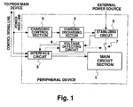
- Fig. 1 is a block diagram illustrating mainly the interface section of the peripheral device according to one embodiment of the present invention.
- the peripheral device includes a main circuit section 1, a charging/discharging section 2, a stabilizing circuit 3, a voltage detecting circuit 4, an interface circuit 5, a charging control section 6, and a power supply switch 7.
- a power feed line and a control signal line come from the main device, such as a personal computer.
- the control signal line is connected to the interface circuit 5, while the power feed line is connected to both the interface circuit 5 and the charging control section 6.
- the main circuit section 1 serves to implement a main function of the peripheral device and operates using electric power supplied from the stabilizing circuit 3 via the power supply switch 7.
- the charging/discharging section 2 may be, for example, a storage battery or a large capacity condenser.
- the charging control section 6 receives electric power from the main device through the power feeding line and charges the charging/discharging section 2.
- the stabilizing circuit 3 supplies electric power fed from the charging/discharging section 2 to the main circuit section via the power supply switch 7.
- the stabilizing circuit 3 stabilizes the output voltage of the charging/discharging section 2, so that a predetermined voltage value is applied to the main circuit section 1 serving as a load, regardless of how the main circuit section 1 operates. If an external power source is provided, the stabilizing circuit 3 receives electric power from the external power source and supplies power to the main circuit section 1 via the power supply switch 7.
- the voltage detecting circuit 4 determines whether the voltage value of the charging/discharging section 2 has reached a predetermined voltage value (i.e., whether the main circuit section 1 is operative), and outputs a signal indicative of the result of determination to the interface circuit 5. Also, the voltage detecting circuit 4 detects the presence or absence of the external power source connected to the stabilizing circuit 3 and, when the external power source is detected, outputs a signal indicating that the main circuit section 1 is operative to the interface circuit 5, regardless of the voltage value of the charging/discharging section 2.
- the interface circuit 5 operates using electric power supplied through the power feed line.
- the interface circuit 5 serves to supply the main circuit section 1 with the control signal received from the main device via the control signal line.
- the interface circuit 5 receives a signal indicating of whether or not the main circuit section 1 is operative from the voltage detecting circuit 4.
- the interface circuit 5 turns on the power supply switch 7 to supply electric power to the main circuit section 1, while supplying the main circuit section 1 with the control signal received via the control signal line.
- the interface circuit 5 turns off the power supply switch 7 to stop feeding electric power to the main circuit section 1.
- the interface circuit 5 transmits a signal indicative of the inoperative state to the main device via the control signal line.
- the signal indicates that the device is not ready. More specifically, the signal indicates that no recording medium is inserted, or that an impossible measurement result value or error information in accordance with a certain protocol predetermined for the main device has been detected.
- a signal indicating that no medium is present is sent when the state of charge (e.g., an output voltage value) of the charging/discharging section 2 is insufficient to operate the main circuit section 1.
- the state of charge e.g., an output voltage value
- a printer for example, even when the printing sheets are already fed, error information indicating "no paper" may be sent.
- a measurement result value an impossible measurement value which exceeds a predetermined value is output in a driver software installed in the main device or the personal computer.
- the interface circuit 5 can send the error information according to the definition, it is possible for the main device to recognize whether or not the peripheral device is ready, regardless of the type of peripheral device.
- the voltage detecting circuit 4 may determine whether or not the main circuit section 1 is operative in response to a request from the interface circuit 5. In such a case, when the control signal is received from the main device, the interface circuit 5 requests the voltage detecting circuit 4 to determine whether or not the main circuit section 1 is operative, and then receives a signal indicative of the result of the determination.
- the peripheral device of this embodiment will be described in detail below using two examples in which an external power source for the peripheral device is not connected. First, operation of the peripheral device when the external power scurce is not connected thereto will be described. At such times, the peripheral device of this embodiment only receives electric power from the main device, such as a personal computer, via the power feed line of the interface cable. Using the electric power supplied through the power feedline, the charging control section 6 charges the charging/discharging section 2.
- the interface circuit 5 requests the voltage detecting circuit 4 to determine whether or not the main circuit section 1 is operative.
- the voltage detecting circuit 4 detects the state of charge, e.g., an output voltage value, of the charging/discharging section 2 and, when it determines that the charged state is sufficient for operating the main circuit section 1, sends a signal indicative of the operative state (shown as an OK signal in the figure) to the interface circuit 5.
- whether or not the main circuit section 1 is operative is determined by comparing the output voltage value with a reference value, and, when the measure value exceeds the reference value, it is determined that the device is in an operative state.
- the interface circuit 5 turns on the power supply switch 7.
- the charging/discharging section 2 supplies electric power to the stabilizing circuit 3 which, in turn, supplies the received electric power to the main circuit section 1 after stabilization.
- the interface circuit 5 outputs the control signal received from the main device to the main circuit section 1. As a result, the main circuit section 1 operates normally. It should be noted that when data is communicated to and from the main device during the operation of the main circuit section 1, the interface circuit 5 mediates the data communication.
- the interface circuit 5 when the interface circuit 5 receives the control signal from the main device and requests the voltage detecting circuit 4 to determine whether or not the main circuit section 1 is operative, the interface circuit 5 turns off the power supply switch 7 if it is determined that the charged state of the charging/discharging section 2 is insufficient for the operation of the main circuit section 1 (shown as an NG signal in the figure). Also, the interface circuit 5 reports the inoperative state of the main circuit section 1 to the main device in response to the control signal. In this manner, the main device can judge whether or not the main circuit section 1 is operative. Here, it should be noted that the interface circuit 5 does not supply any control signal to the main circuit section 1.
- the peripheral device of this example receives electric power from the main device or the personal computer via the power feed line of the interface cable.
- the charging control section 6 uses the electric power supplied through the power feeding line to charge the charging/discharging section 2.
- the interface circuit 5 when a control signal is received from the main device, the interface circuit 5 requests the voltage detecting circuit 4 to determine whether or not the main circuit section 1 is operative. In response to this request, the voltage detecting circuit 4 detects that the external power source is connected to the stabilizing circuit 3 and sends to the interface circuit 5 a signal indicating that the main circuit section 1 is operative. Then, the interface circuit turns on the power supply switch 7. The stabilizing circuit 3 stabilizes electric power supplied from the external power source and supplies it to the main circuit section 1. The interface circuit 5 also transfers the control signal received from the main device to the main circuit section 1. As a result, the main circuit section 1 operates normally. It should be noted that if data is communicated to and from the main device during the operation of the main circuit section 1, the interface circuit 5 mediates the data communication.
- the peripheral device charges the internal charging/discharging section 2 with electric power supplied from the main device via the interface cable and, when a start-up instruction is received from the main device, detects the state of charge of the charging/discharging section 2.
- the peripheral device operates the main circuit section 1 if it is operative, or if the main circuit section 1 is inoperative, sends to the main device a signal (i.e., an error signal) indicative of inoperative state of the main circuit section.
- the main circuit section 1 is operated in response to the start-up instruction from the main device, irrespective of the state of charge of the charging/discharging section 2.
- the interface circuit 5 which operates using electric power supplied from the main device, can transmit the error signal to the main device when the charging/discharging section 2 is insufficiently charged.
- the main device can recognize the abnormal condition of the peripheral device based on the error signal, enabling proper control of the device.
- the voltage detecting circuit 4 may regularly detect the charged state of the charging/discharging section 2 and output a signal to the interface circuit 5 to indicate when the main circuit section 1 switches from the inoperative state to the operative state. In response to such a signal, the interface circuit 5 reports the operative state to the main device. In this manner, the main device can properly control the peripheral device of this embodiment based on the state of the peripheral device.
- the power supply switch 7 may not be provided.
- An example of such a configuration is shown in Fig. 4.
- the interface circuit 5 instead of using the signal for turning on/off the power supply switch 7, the interface circuit 5 outputs an instruction to enter or exist the sleep mode. Effects and advantages will be similar to those of the above-described examples of the embodiment.
- the voltage detecting circuit 4 detects the charged state of the charging/discharging section 2 and, when it is determined that the main circuit section 1 is inoperative, outputs an NG signal to the interface circuit 5.
- the interface circuit 5 sends the error signal to the main device via the control signal line, while sending a signal ordering the main circuit section 1 to shift to sleep mode.
- the voltage detecting circuit 4 outputs an OK signal to the interface circuit 5.
- the interface circuit 5, in turn, sends a resume signal to the main circuit section 1 so that it can awaken from the sleep mode and resume the operation mode.
- the voltage detecting circuit 4 detects the state of charge of the charging/discharging section 2 and determines the operation capability of the main circuit section 1 based on the detected state of charge
- the voltage detecting circuit 4 may detect only an output voltage of the charging/discharging section 2 and send the output voltage value to the interface circuit 5 so that the interface circuit 5 can determine whether or not the main circuit section 1 is operative. It is possible to fabricate both the voltage detecting circuit 4 and the interface circuit 5 as a single IC circuit.
- the present invention provides a peripheral device which reliably reports errors to a main device. When a control signal is received from the main device, an interface circuit requests a voltage detecting circuit to determine whether or not a main circuit section is operative.
- the voltage detecting circuit determines the capability of operation of the main circuit section based on the state of charge of a charging/discharging section, and outputs the results to the interface circuit. If determined to be operative, the interface circuit turns on a power supply switch to operate the main circuit section, while outputting the control signal received from the main device to the main circuit section. If inoperative, the interface circuit transmits to the main device a signal informing it of the inoperative state.
Landscapes
- Engineering & Computer Science (AREA)
- General Engineering & Computer Science (AREA)
- Theoretical Computer Science (AREA)
- Computer Hardware Design (AREA)
- Physics & Mathematics (AREA)
- General Physics & Mathematics (AREA)
- Power Sources (AREA)
- Direct Current Feeding And Distribution (AREA)
Applications Claiming Priority (2)
| Application Number | Priority Date | Filing Date | Title |
|---|---|---|---|
| JP2001126632A JP2002323941A (ja) | 2001-04-24 | 2001-04-24 | 周辺装置 |
| JP2001126632 | 2001-04-24 |
Publications (2)
| Publication Number | Publication Date |
|---|---|
| EP1253508A2 true EP1253508A2 (de) | 2002-10-30 |
| EP1253508A3 EP1253508A3 (de) | 2005-06-22 |
Family
ID=18975635
Family Applications (1)
| Application Number | Title | Priority Date | Filing Date |
|---|---|---|---|
| EP02008962A Withdrawn EP1253508A3 (de) | 2001-04-24 | 2002-04-22 | Peripheriegerät |
Country Status (3)
| Country | Link |
|---|---|
| US (1) | US20020157039A1 (de) |
| EP (1) | EP1253508A3 (de) |
| JP (1) | JP2002323941A (de) |
Cited By (1)
| Publication number | Priority date | Publication date | Assignee | Title |
|---|---|---|---|---|
| CN105531157A (zh) * | 2013-09-11 | 2016-04-27 | 株式会社电装 | 车载装置、车载通信系统 |
Families Citing this family (5)
| Publication number | Priority date | Publication date | Assignee | Title |
|---|---|---|---|---|
| US7212067B2 (en) * | 2003-08-01 | 2007-05-01 | Sandisk Corporation | Voltage regulator with bypass for multi-voltage storage system |
| US7164561B2 (en) * | 2004-02-13 | 2007-01-16 | Sandisk Corporation | Voltage regulator using protected low voltage devices |
| US7391193B2 (en) * | 2005-01-25 | 2008-06-24 | Sandisk Corporation | Voltage regulator with bypass mode |
| JP2007156605A (ja) * | 2005-12-01 | 2007-06-21 | I-O Data Device Inc | 外付け周辺装置及びインタフェースケーブル |
| US8037331B2 (en) * | 2008-04-28 | 2011-10-11 | Dell Products L.P. | Energy efficient method to wake host system for charging battery powered portable devices via bus powered external i/o ports |
Family Cites Families (14)
| Publication number | Priority date | Publication date | Assignee | Title |
|---|---|---|---|---|
| US4689698A (en) * | 1983-07-11 | 1987-08-25 | Brother Kogyo Kabushiki Kaisha | Disk drive control for inhibiting operation upon battery voltage drop |
| WO1997003473A1 (fr) * | 1995-07-10 | 1997-01-30 | International Business Machines Corporation | Dispositif de boitier pour bloc batterie et bloc batterie |
| US5675813A (en) * | 1995-10-26 | 1997-10-07 | Microsoft Corporation | System and method for power control in a universal serial bus |
| US5969529A (en) * | 1996-03-14 | 1999-10-19 | Sharp Kabushiki Kaisha | Electronic apparatus having battery power source |
| US6138178A (en) * | 1997-01-29 | 2000-10-24 | Fuji Photo Film Co., Ltd. | Controlled device storing multiple drivers that judges and downloads a particular driver corresponding to a controller's operating system having an identical or greater version number |
| JP4400937B2 (ja) * | 1997-09-29 | 2010-01-20 | 株式会社ルネサステクノロジ | Usbデバイス |
| JP2000029544A (ja) * | 1998-07-09 | 2000-01-28 | Canon Inc | 電源制御装置、usb装置、及び電源制御方法 |
| US6715071B2 (en) * | 1998-06-26 | 2004-03-30 | Canon Kabushiki Kaisha | System having devices connected via communication lines |
| JP2000020175A (ja) * | 1998-06-26 | 2000-01-21 | Toshiba Corp | 電子機器 |
| US6357011B2 (en) * | 1998-07-15 | 2002-03-12 | Gateway, Inc. | Bus-powered computer peripheral with supplement battery power to overcome bus-power limit |
| DE19944053C2 (de) * | 1999-09-14 | 2001-08-02 | Infineon Technologies Ag | Vorrichtung und Verfahren zur Stromversorgung von Rechner-Zusatzgeräten über das Bussystem des Rechners |
| US6665801B1 (en) * | 2000-01-27 | 2003-12-16 | Symbol Technologies, Inc. | Method and apparatus for charging a self powered USB device at different charge rates according to the charge level of a rechargeable element on the device |
| JP4450962B2 (ja) * | 2000-08-21 | 2010-04-14 | オリンパス株式会社 | プリンタ装置 |
| US6465987B1 (en) * | 2000-10-17 | 2002-10-15 | Hewlett-Packard Company | Power source of peripheral devices |
-
2001
- 2001-04-24 JP JP2001126632A patent/JP2002323941A/ja active Pending
-
2002
- 2002-04-12 US US10/120,555 patent/US20020157039A1/en not_active Abandoned
- 2002-04-22 EP EP02008962A patent/EP1253508A3/de not_active Withdrawn
Cited By (2)
| Publication number | Priority date | Publication date | Assignee | Title |
|---|---|---|---|---|
| CN105531157A (zh) * | 2013-09-11 | 2016-04-27 | 株式会社电装 | 车载装置、车载通信系统 |
| CN105531157B (zh) * | 2013-09-11 | 2017-07-28 | 株式会社电装 | 车载装置、车载通信系统 |
Also Published As
| Publication number | Publication date |
|---|---|
| EP1253508A3 (de) | 2005-06-22 |
| US20020157039A1 (en) | 2002-10-24 |
| JP2002323941A (ja) | 2002-11-08 |
Similar Documents
| Publication | Publication Date | Title |
|---|---|---|
| US7653772B2 (en) | Control system, electronic device and image forming apparatus | |
| US7283262B2 (en) | Image forming apparatus and power control method | |
| CN102006385B (zh) | 图像形成设备 | |
| US7631200B2 (en) | Host apparatus, device, and method for controlling communication system | |
| US6895196B2 (en) | Image forming apparatus having reduced power consumption mode and control method therefor | |
| US8549337B2 (en) | Memory card control device and method for controlling the same | |
| US11755089B2 (en) | Information processing apparatus, electric power transfer system, control method of information processing apparatus, and non-transitory computer-readable storage medium | |
| JPH10164668A (ja) | データ通信システム及びデータ通信装置並びにデータ通信制御プログラムを記録した記録媒体 | |
| EP1253508A2 (de) | Peripheriegerät | |
| US10158771B2 (en) | Information processing apparatus that transfers diagnosis information on a unit to another unit through a communication line for CPU to CPU communication, method of controlling an information processing apparatus, and storage medium | |
| US11750015B2 (en) | Information processing apparatus, control method of information processing apparatus, and non-transitory computer-readable storage medium | |
| JP2001337752A (ja) | ホスト装置の周辺デバイス | |
| US6286107B1 (en) | Method and apparatus for signal interfacing capable of infallibly notifying a status of an apparatus | |
| JP2003316558A (ja) | 印刷装置の制御方法、印刷装置の制御プログラム、印刷装置の制御プログラムを記録した記録媒体、及び印刷システム | |
| JP3739581B2 (ja) | インタフェイス装置 | |
| JP2004029893A (ja) | 記録装置 | |
| US20070070387A1 (en) | Image forming apparatus, additional apparatus connectable to image forming apparatus, image forming system, and control method thereof | |
| JP2004094821A (ja) | 記録装置 | |
| JP3346289B2 (ja) | 電力供給システムおよび電力供給方法 | |
| KR101545317B1 (ko) | 차량 운행정보 전송용 스마트 태블릿의 전원 제어 장치 및 그 방법 | |
| US20040085308A1 (en) | Apparatus and method for controlling power of monitor | |
| JP3576387B2 (ja) | 半導体回路および同回路を備えた移動体識別装置 | |
| JP2007160679A (ja) | インクジェットプリンタおよび画像形成装置と制御方法 | |
| JPH0542217B2 (de) | ||
| JP2004363920A (ja) | 画像形成システム |
Legal Events
| Date | Code | Title | Description |
|---|---|---|---|
| PUAI | Public reference made under article 153(3) epc to a published international application that has entered the european phase |
Free format text: ORIGINAL CODE: 0009012 |
|
| AK | Designated contracting states |
Kind code of ref document: A2 Designated state(s): AT BE CH CY DE DK ES FI FR GB GR IE IT LI LU MC NL PT SE TR |
|
| AX | Request for extension of the european patent |
Free format text: AL;LT;LV;MK;RO;SI |
|
| PUAL | Search report despatched |
Free format text: ORIGINAL CODE: 0009013 |
|
| AK | Designated contracting states |
Kind code of ref document: A3 Designated state(s): AT BE CH CY DE DK ES FI FR GB GR IE IT LI LU MC NL PT SE TR |
|
| AX | Request for extension of the european patent |
Extension state: AL LT LV MK RO SI |
|
| RIC1 | Information provided on ipc code assigned before grant |
Ipc: 7G 06F 1/32 B Ipc: 7G 06F 1/26 A |
|
| AKX | Designation fees paid | ||
| STAA | Information on the status of an ep patent application or granted ep patent |
Free format text: STATUS: THE APPLICATION IS DEEMED TO BE WITHDRAWN |
|
| 18D | Application deemed to be withdrawn |
Effective date: 20051223 |
|
| REG | Reference to a national code |
Ref country code: DE Ref legal event code: 8566 |