EP1248503A1 - Multilayer printed wiring board and method of manufacturing the same - Google Patents
Multilayer printed wiring board and method of manufacturing the same Download PDFInfo
- Publication number
- EP1248503A1 EP1248503A1 EP00987672A EP00987672A EP1248503A1 EP 1248503 A1 EP1248503 A1 EP 1248503A1 EP 00987672 A EP00987672 A EP 00987672A EP 00987672 A EP00987672 A EP 00987672A EP 1248503 A1 EP1248503 A1 EP 1248503A1
- Authority
- EP
- European Patent Office
- Prior art keywords
- copper
- wiring board
- multilayer printed
- printed wiring
- etching
- Prior art date
- Legal status (The legal status is an assumption and is not a legal conclusion. Google has not performed a legal analysis and makes no representation as to the accuracy of the status listed.)
- Withdrawn
Links
- 238000004519 manufacturing process Methods 0.000 title claims abstract description 54
- RYGMFSIKBFXOCR-UHFFFAOYSA-N Copper Chemical compound [Cu] RYGMFSIKBFXOCR-UHFFFAOYSA-N 0.000 claims abstract description 125
- 238000005530 etching Methods 0.000 claims abstract description 92
- 239000010949 copper Substances 0.000 claims abstract description 82
- 229910052802 copper Inorganic materials 0.000 claims abstract description 77
- PXHVJJICTQNCMI-UHFFFAOYSA-N Nickel Chemical compound [Ni] PXHVJJICTQNCMI-UHFFFAOYSA-N 0.000 claims abstract description 72
- 238000005253 cladding Methods 0.000 claims abstract description 59
- 239000011889 copper foil Substances 0.000 claims abstract description 49
- 239000004020 conductor Substances 0.000 claims abstract description 39
- 239000000463 material Substances 0.000 claims description 67
- 229910052759 nickel Inorganic materials 0.000 claims description 30
- 239000011347 resin Substances 0.000 claims description 29
- 229920005989 resin Polymers 0.000 claims description 29
- 239000011248 coating agent Substances 0.000 claims description 24
- 238000000576 coating method Methods 0.000 claims description 24
- 238000007747 plating Methods 0.000 claims description 20
- BQCADISMDOOEFD-UHFFFAOYSA-N Silver Chemical compound [Ag] BQCADISMDOOEFD-UHFFFAOYSA-N 0.000 claims description 18
- 229910052709 silver Inorganic materials 0.000 claims description 11
- 239000004332 silver Substances 0.000 claims description 11
- 238000000034 method Methods 0.000 claims description 7
- 239000010410 layer Substances 0.000 description 68
- 239000000243 solution Substances 0.000 description 12
- 239000007864 aqueous solution Substances 0.000 description 6
- 229920002120 photoresistant polymer Polymers 0.000 description 5
- 239000003822 epoxy resin Substances 0.000 description 4
- 239000011888 foil Substances 0.000 description 4
- 229920000647 polyepoxide Polymers 0.000 description 4
- 229920001721 polyimide Polymers 0.000 description 4
- 239000009719 polyimide resin Substances 0.000 description 4
- 230000004913 activation Effects 0.000 description 3
- 238000007598 dipping method Methods 0.000 description 3
- 239000011229 interlayer Substances 0.000 description 3
- 238000010030 laminating Methods 0.000 description 3
- 239000004065 semiconductor Substances 0.000 description 3
- 238000000992 sputter etching Methods 0.000 description 3
- MHAJPDPJQMAIIY-UHFFFAOYSA-N Hydrogen peroxide Chemical compound OO MHAJPDPJQMAIIY-UHFFFAOYSA-N 0.000 description 2
- QAOWNCQODCNURD-UHFFFAOYSA-N Sulfuric acid Chemical compound OS(O)(=O)=O QAOWNCQODCNURD-UHFFFAOYSA-N 0.000 description 2
- 238000007772 electroless plating Methods 0.000 description 2
- 230000002708 enhancing effect Effects 0.000 description 2
- VCJMYUPGQJHHFU-UHFFFAOYSA-N iron(3+);trinitrate Chemical compound [Fe+3].[O-][N+]([O-])=O.[O-][N+]([O-])=O.[O-][N+]([O-])=O VCJMYUPGQJHHFU-UHFFFAOYSA-N 0.000 description 2
- 238000005507 spraying Methods 0.000 description 2
- QGZKDVFQNNGYKY-UHFFFAOYSA-O Ammonium Chemical compound [NH4+] QGZKDVFQNNGYKY-UHFFFAOYSA-O 0.000 description 1
- 238000005520 cutting process Methods 0.000 description 1
- 238000005516 engineering process Methods 0.000 description 1
- 239000001257 hydrogen Substances 0.000 description 1
- 229910052739 hydrogen Inorganic materials 0.000 description 1
- 125000004435 hydrogen atom Chemical class [H]* 0.000 description 1
- 239000011261 inert gas Substances 0.000 description 1
- 230000010354 integration Effects 0.000 description 1
- 238000003475 lamination Methods 0.000 description 1
- 239000002184 metal Substances 0.000 description 1
- 229910052751 metal Inorganic materials 0.000 description 1
- 150000004968 peroxymonosulfuric acids Chemical class 0.000 description 1
- 238000005498 polishing Methods 0.000 description 1
- 239000002994 raw material Substances 0.000 description 1
- 238000005096 rolling process Methods 0.000 description 1
- 230000008054 signal transmission Effects 0.000 description 1
- 239000002344 surface layer Substances 0.000 description 1
Images




Classifications
-
- H—ELECTRICITY
- H05—ELECTRIC TECHNIQUES NOT OTHERWISE PROVIDED FOR
- H05K—PRINTED CIRCUITS; CASINGS OR CONSTRUCTIONAL DETAILS OF ELECTRIC APPARATUS; MANUFACTURE OF ASSEMBLAGES OF ELECTRICAL COMPONENTS
- H05K3/00—Apparatus or processes for manufacturing printed circuits
- H05K3/46—Manufacturing multilayer circuits
-
- H—ELECTRICITY
- H05—ELECTRIC TECHNIQUES NOT OTHERWISE PROVIDED FOR
- H05K—PRINTED CIRCUITS; CASINGS OR CONSTRUCTIONAL DETAILS OF ELECTRIC APPARATUS; MANUFACTURE OF ASSEMBLAGES OF ELECTRICAL COMPONENTS
- H05K1/00—Printed circuits
- H05K1/02—Details
- H05K1/0213—Electrical arrangements not otherwise provided for
- H05K1/0216—Reduction of cross-talk, noise or electromagnetic interference
- H05K1/0218—Reduction of cross-talk, noise or electromagnetic interference by printed shielding conductors, ground planes or power plane
- H05K1/0219—Printed shielding conductors for shielding around or between signal conductors, e.g. coplanar or coaxial printed shielding conductors
- H05K1/0221—Coaxially shielded signal lines comprising a continuous shielding layer partially or wholly surrounding the signal lines
-
- H—ELECTRICITY
- H05—ELECTRIC TECHNIQUES NOT OTHERWISE PROVIDED FOR
- H05K—PRINTED CIRCUITS; CASINGS OR CONSTRUCTIONAL DETAILS OF ELECTRIC APPARATUS; MANUFACTURE OF ASSEMBLAGES OF ELECTRICAL COMPONENTS
- H05K3/00—Apparatus or processes for manufacturing printed circuits
- H05K3/02—Apparatus or processes for manufacturing printed circuits in which the conductive material is applied to the surface of the insulating support and is thereafter removed from such areas of the surface which are not intended for current conducting or shielding
- H05K3/06—Apparatus or processes for manufacturing printed circuits in which the conductive material is applied to the surface of the insulating support and is thereafter removed from such areas of the surface which are not intended for current conducting or shielding the conductive material being removed chemically or electrolytically, e.g. by photo-etch process
- H05K3/061—Etching masks
- H05K3/062—Etching masks consisting of metals or alloys or metallic inorganic compounds
-
- H—ELECTRICITY
- H05—ELECTRIC TECHNIQUES NOT OTHERWISE PROVIDED FOR
- H05K—PRINTED CIRCUITS; CASINGS OR CONSTRUCTIONAL DETAILS OF ELECTRIC APPARATUS; MANUFACTURE OF ASSEMBLAGES OF ELECTRICAL COMPONENTS
- H05K2201/00—Indexing scheme relating to printed circuits covered by H05K1/00
- H05K2201/03—Conductive materials
- H05K2201/0332—Structure of the conductor
- H05K2201/0335—Layered conductors or foils
- H05K2201/0361—Etched tri-metal structure, i.e. metal layers or metal patterns on both sides of a different central metal layer which is later at least partly etched
-
- H—ELECTRICITY
- H05—ELECTRIC TECHNIQUES NOT OTHERWISE PROVIDED FOR
- H05K—PRINTED CIRCUITS; CASINGS OR CONSTRUCTIONAL DETAILS OF ELECTRIC APPARATUS; MANUFACTURE OF ASSEMBLAGES OF ELECTRICAL COMPONENTS
- H05K2201/00—Indexing scheme relating to printed circuits covered by H05K1/00
- H05K2201/09—Shape and layout
- H05K2201/09209—Shape and layout details of conductors
- H05K2201/09218—Conductive traces
- H05K2201/09254—Branched layout
-
- H—ELECTRICITY
- H05—ELECTRIC TECHNIQUES NOT OTHERWISE PROVIDED FOR
- H05K—PRINTED CIRCUITS; CASINGS OR CONSTRUCTIONAL DETAILS OF ELECTRIC APPARATUS; MANUFACTURE OF ASSEMBLAGES OF ELECTRICAL COMPONENTS
- H05K2203/00—Indexing scheme relating to apparatus or processes for manufacturing printed circuits covered by H05K3/00
- H05K2203/03—Metal processing
- H05K2203/0384—Etch stop layer, i.e. a buried barrier layer for preventing etching of layers under the etch stop layer
-
- H—ELECTRICITY
- H05—ELECTRIC TECHNIQUES NOT OTHERWISE PROVIDED FOR
- H05K—PRINTED CIRCUITS; CASINGS OR CONSTRUCTIONAL DETAILS OF ELECTRIC APPARATUS; MANUFACTURE OF ASSEMBLAGES OF ELECTRICAL COMPONENTS
- H05K2203/00—Indexing scheme relating to apparatus or processes for manufacturing printed circuits covered by H05K3/00
- H05K2203/07—Treatments involving liquids, e.g. plating, rinsing
- H05K2203/0703—Plating
- H05K2203/0733—Method for plating stud vias, i.e. massive vias formed by plating the bottom of a hole without plating on the walls
-
- H—ELECTRICITY
- H05—ELECTRIC TECHNIQUES NOT OTHERWISE PROVIDED FOR
- H05K—PRINTED CIRCUITS; CASINGS OR CONSTRUCTIONAL DETAILS OF ELECTRIC APPARATUS; MANUFACTURE OF ASSEMBLAGES OF ELECTRICAL COMPONENTS
- H05K3/00—Apparatus or processes for manufacturing printed circuits
- H05K3/46—Manufacturing multilayer circuits
- H05K3/4644—Manufacturing multilayer circuits by building the multilayer layer by layer, i.e. build-up multilayer circuits
- H05K3/4647—Manufacturing multilayer circuits by building the multilayer layer by layer, i.e. build-up multilayer circuits by applying an insulating layer around previously made via studs
-
- Y—GENERAL TAGGING OF NEW TECHNOLOGICAL DEVELOPMENTS; GENERAL TAGGING OF CROSS-SECTIONAL TECHNOLOGIES SPANNING OVER SEVERAL SECTIONS OF THE IPC; TECHNICAL SUBJECTS COVERED BY FORMER USPC CROSS-REFERENCE ART COLLECTIONS [XRACs] AND DIGESTS
- Y10—TECHNICAL SUBJECTS COVERED BY FORMER USPC
- Y10T—TECHNICAL SUBJECTS COVERED BY FORMER US CLASSIFICATION
- Y10T29/00—Metal working
- Y10T29/49—Method of mechanical manufacture
- Y10T29/49002—Electrical device making
- Y10T29/49117—Conductor or circuit manufacturing
- Y10T29/49124—On flat or curved insulated base, e.g., printed circuit, etc.
- Y10T29/49126—Assembling bases
-
- Y—GENERAL TAGGING OF NEW TECHNOLOGICAL DEVELOPMENTS; GENERAL TAGGING OF CROSS-SECTIONAL TECHNOLOGIES SPANNING OVER SEVERAL SECTIONS OF THE IPC; TECHNICAL SUBJECTS COVERED BY FORMER USPC CROSS-REFERENCE ART COLLECTIONS [XRACs] AND DIGESTS
- Y10—TECHNICAL SUBJECTS COVERED BY FORMER USPC
- Y10T—TECHNICAL SUBJECTS COVERED BY FORMER US CLASSIFICATION
- Y10T29/00—Metal working
- Y10T29/49—Method of mechanical manufacture
- Y10T29/49002—Electrical device making
- Y10T29/49117—Conductor or circuit manufacturing
- Y10T29/49124—On flat or curved insulated base, e.g., printed circuit, etc.
- Y10T29/4913—Assembling to base an electrical component, e.g., capacitor, etc.
-
- Y—GENERAL TAGGING OF NEW TECHNOLOGICAL DEVELOPMENTS; GENERAL TAGGING OF CROSS-SECTIONAL TECHNOLOGIES SPANNING OVER SEVERAL SECTIONS OF THE IPC; TECHNICAL SUBJECTS COVERED BY FORMER USPC CROSS-REFERENCE ART COLLECTIONS [XRACs] AND DIGESTS
- Y10—TECHNICAL SUBJECTS COVERED BY FORMER USPC
- Y10T—TECHNICAL SUBJECTS COVERED BY FORMER US CLASSIFICATION
- Y10T29/00—Metal working
- Y10T29/49—Method of mechanical manufacture
- Y10T29/49002—Electrical device making
- Y10T29/49117—Conductor or circuit manufacturing
- Y10T29/49124—On flat or curved insulated base, e.g., printed circuit, etc.
- Y10T29/49147—Assembling terminal to base
- Y10T29/49151—Assembling terminal to base by deforming or shaping
-
- Y—GENERAL TAGGING OF NEW TECHNOLOGICAL DEVELOPMENTS; GENERAL TAGGING OF CROSS-SECTIONAL TECHNOLOGIES SPANNING OVER SEVERAL SECTIONS OF THE IPC; TECHNICAL SUBJECTS COVERED BY FORMER USPC CROSS-REFERENCE ART COLLECTIONS [XRACs] AND DIGESTS
- Y10—TECHNICAL SUBJECTS COVERED BY FORMER USPC
- Y10T—TECHNICAL SUBJECTS COVERED BY FORMER US CLASSIFICATION
- Y10T29/00—Metal working
- Y10T29/49—Method of mechanical manufacture
- Y10T29/49002—Electrical device making
- Y10T29/49117—Conductor or circuit manufacturing
- Y10T29/49124—On flat or curved insulated base, e.g., printed circuit, etc.
- Y10T29/49155—Manufacturing circuit on or in base
-
- Y—GENERAL TAGGING OF NEW TECHNOLOGICAL DEVELOPMENTS; GENERAL TAGGING OF CROSS-SECTIONAL TECHNOLOGIES SPANNING OVER SEVERAL SECTIONS OF THE IPC; TECHNICAL SUBJECTS COVERED BY FORMER USPC CROSS-REFERENCE ART COLLECTIONS [XRACs] AND DIGESTS
- Y10—TECHNICAL SUBJECTS COVERED BY FORMER USPC
- Y10T—TECHNICAL SUBJECTS COVERED BY FORMER US CLASSIFICATION
- Y10T29/00—Metal working
- Y10T29/49—Method of mechanical manufacture
- Y10T29/49002—Electrical device making
- Y10T29/49117—Conductor or circuit manufacturing
- Y10T29/49124—On flat or curved insulated base, e.g., printed circuit, etc.
- Y10T29/49155—Manufacturing circuit on or in base
- Y10T29/49156—Manufacturing circuit on or in base with selective destruction of conductive paths
Definitions
- the present invention relates to a structure of a multilayer printed wiring board, a cladding sheet used therefor and a method of manufacturing a multilayer printed wiring board having the structure, particularly to an electric circuit connector of a connector pin or the like.
- the proposal is a multilayer printed wiring board comprising a film adhering base material laminatedly constituted by a copper-clad laminated sheet formed with an earth circuit conductor and a film-like copper-clad laminated sheet formed with an earth circuit conductor and a signal circuit conductor, and a through hole, forming a coaxial circuit structure on the wiring board.
- a coaxial circuit having a strip structure in which the signal circuit conductor is completely covered by the earth circuit conductor and a via hole for interlayer connection between inner layers can also be provided, and there can be provided a multilayer printed wiring board constituting a high speed signal transmission line which is not effected with influence of radiated noise or crosstalk noise.
- the multilayer printed wiring board is provided with a hole of through hole for interlayer connection.
- a method of manufacturing the multilayer printed wiring board firstly, a copper-clad laminated sheet formed with an earth circuit conductor and a film-like copper-clad laminated sheet formed with an earth circuit conductor and a signal circuit conductor, are fabricated separately from each other, and laminated to each other to thereby construct a constitution of an integrated-type circuit structure of a coaxial structure and by perforating the structure for constituting a through hole and inserting a shortcircuit pin provided with a contact point into a necessary one of the through hole, an apparatus board or the like can be set and a via hole for interlayer connection between inner layers is formed not by perforating but by copper plating and etching treatment.
- the inventors have finished the invention by reaching a conclusion that it is mostly preferable to adopt a manufacturing method of manufacturing a total of a wiring board by an etching treatment and providing a wiring lead-out port at the stage.
- a multilayer printed wiring board according to the invention is characterized in including a signal circuit conductor completely covered by an earth circuit at an inner portion thereof as well as providing a lead-out port.
- the wiring lead-out port can easily be formed and a large amount of products can easily be processed with good dimension reproducibility.
- the signal circuit conductor includes a branch pattern.
- a method of fabricating a multilayer printed wiring board according to the invention is characterized by forming a signal circuit conductor completely covered by an earth circuit at an inner portion thereof and a wiring lead-out port by selective etching of copper with regard to a cladding sheet for the multilayer printed wiring board manufactured by bringing a copper foil material and a nickel foil material into press contact with each other by a reduction ratio of 0.1 to 3 %.
- the cladding sheet for the multilayer printed wiring board comprises five layers of copper/nickel/copper/nickel/copper.
- the cladding sheet for the multilayer printed wiring board is manufactured by bringing the copper foil material provided with nickel plating at one face or two faces thereof and other copper foil material or a copper foil material provided with nickel plating at one face thereof into press contact with each other by the reduction ratio of 0.1 to 3 %.
- a method of fabricating a multilayer printed wiring board according to the invention is characterized in forming a signal circuit conductor completely covered by an earth circuit at an inner portion thereof by selective etching of copper with regard to a cladding sheet for the multilayer printed wiring board manufactured by bringing a copper foil material and a silver foil material into press contact with each other by a reduction ratio of 0.1 to 3 %.
- the cladding sheet for the multilayer printed wiring board comprises three layers of copper/silver/copper.
- the cladding sheet for the multilayer printed wiring board is manufactured by bringing a copper foil material provided with silver plating at one face thereof and other copper foil material into press contact with each other by a reduction ratio of 0.1 to 3 %.
- the manufacturing method is carried out by forming a resist pattern for forming a circuit shield wall and for forming a wiring lead-out port at the copper layer on the one face of the cladding sheet for the multilayer printed wiring board, thereafter carrying out selective etching of copper to thereby form the circuit shield wall and the wiring lead-out port, removing the nickel layer, successively coating an insulating resin on an etching face, thereafter forming a resist pattern for forming a circuit shield wall at a copper layer on a rear face of the cladding sheet, thereafter carrying out selective etching of copper to thereby form the circuit shield wall, etching the intermediate copper layer to thereby form a signal circuit, coating an insulating resin on an etching face and plating copper on two faces thereof to thereby form the shield wall.
- the manufacturing method is carried out by forming a resist pattern for forming a circuit shield wall or for forming the wiring lead-out port at the copper layer on one face of the cladding sheet with regard to the cladding sheet for a multilayer printed wiring board, thereafter carrying out selective etching of copper to thereby form the circuit shield wall, successively coating an insulating resin on an etching face, thereafter forming a resist pattern for forming a circuit shield wall at the copper layer on a rear face of the cladding sheet, thereafter carrying out selective etching of copper to thereby form the circuit shield wall, forming a signal circuit by etching the intermediary copper layer, coating an insulating resin on an etching face and thereafer plating copper at other than a portion for constituting a wiring lead-out port to thereby form the shield wall.
- the signal circuit conductor is constituted by a shape including a branch pattern.
- a method of forming a wiring lead-out port in a multilayer printed wiring board is characterized in forming a resist pattern for forming the wiring lead-out port at a copper layer on one face of a cladding sheet for a multilayer printed wiring board, thereafter carrying out selective etching of copper to thereby form a shield wall of the wiring lead-out port, removing a nickel layer, successively coating an insulating resin on an etching face, thereafter etching a copper layer on a rear face of the cladding sheet and coating an insulating resin on an etching face.
- a method of forming a wiring lead-out port in a multilayer printed wiring board is characterized in forming a resist pattern for forming the wiring lead-out port at a copper layer on one face of a cladding sheet for the multilayer printed wiring board, thereafter carrying out selective etching of copper to thereby form a shield wall of the wiring lead-out port, thereafter successively coating an insulating resin on an etching face, thereafter etching a copper layer on a rear face of the cladding sheet to thereby form a circuit shield wall, forming a signal circuit by etching the intermediary silver layer and coating an insulating resin on an etching face.
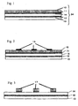
- Fig. 1 is an explanatory view of steps of a method of manufacturing a multilayer printed wiring board according to the invention and is a side view of a cladding sheet for the multilayer printed wiring board.
- Fig. 2 is an explanatory view of steps of a method of manufacturing a multiple printed wiring board according to the invention and is a side view when a resist is coated on a cladding sheet for the multilayer printed wiring board.
- Fig. 3 is an explanatory view of steps of a method of manufacturing a multilayer printed wiring board according to the invention and is a side view after selective etching of copper and removing a nickel layer.
- Fig. 1 is an explanatory view of steps of a method of manufacturing a multilayer printed wiring board according to the invention and is a side view of a cladding sheet for the multilayer printed wiring board.
- Fig. 2 is an explanatory view of steps of a method of manufacturing a multiple printed wiring board according to the invention and is a side view when a resist is coated on
- Fig. 4 is an explanatory view of steps of a method of manufacturing a multilayer printed wiring board according to the invention and is a side view when insulating resin is coated.
- Fig. 5 is an explanatory view of steps of a method of manufacturing a multilayer printed wiring board according to the invention and is a side view when a resist is coated.
- Fig. 6 is an explanatory view of steps of a method of manufacturing a multilayer printed wiring board according to the invention and is a side view after selective etching of copper and removing a nickel layer.
- Fig. 7 is an explanatory view of steps of a method of manufacturing a multilayer printed wiring board according to the invention and is a side view when a resist is coated.
- Fig. 8 is an explanatory view of steps of a method of manufacturing a multilayer printed wiring board according to the invention and is a side view after copper etching.
- Fig. 9 is an explanatory view of steps of a method of manufacturing a multilayer printed wiring board according to the invention and is a side view after coating insulating resin.
- Fig. 10 is an explanatory view of steps of a method of manufacturing a multilayer printed wiring board according to the invention and is a side view after coating copper by electroless plating.
- Fig. 11 is an explanatory view of steps of a method of manufacturing a multilayer printed wiring board according to the invention and is a side view of a cladding sheet for a multilayer printed wiring board.
- Fig. 12 is an explanatory view of steps of a method of manufacturing a multilayer printed wiring board according to the invention and is a side view after coating a resist.
- Fig. 13 is an explanatory view of steps of a method of manufacturing a multilayer printed wiring board according to the invention and is a side view after coating insulating resin and coating a resist.
- Fig. 14 is an explanatory view of steps of a method of manufacturing a multilayer printed wiring board according to the invention and is a side view after etching and coating insulating resin.
- Fig. 15 is an explanatory view of steps of a method of manufacturing a multilayer printed wiring board according to the invention and is a side view after plating copper by electroless plating.
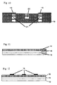
- FIG. 16 is a perspective view of a portion of a wiring lead-out port of a multilayer printed wiring board according to the invention.
- Fig. 17 is a plane view showing a resist pattern when a wiring board branched in a multilayer printed wiring board according to the invention is intended to form.
- Fig. 18 is a three-dimensional view showing a state after etching when a wiring board branched in a multilayer printed wiring board according to the invention is intended to form.
- Fig. 19 is a three-dimensional view showing an example of a signal circuit of a wiring board branched in a multilayer printed wiring board according to the invention.
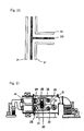
- Fig. 20 is a plane view showing an example of a signal circuit of a wiring board branched in a multilayer printed wiring board according to the invention.
- Fig. 21 is a front sectional view of an apparatus of manufacturing a cladding metal sheet according to the invention.
- the invention provides a multilayer printed wiring board characterized in including a signal circuit conductor completely covered by an earth circuit at an inner portion thereof and providing a wiring lead-out port.
- a multilayer printed wiring board according to the invention can be manufactured as follows.
- a cladding sheet for a printed wiring board.
- a cladding sheet for a printed wiring board a cladding sheet comprising a combination of a copper (Cu) foil material and a nickel (Ni) foil material, for example, a constitution comprising five layers of Cu/Ni/Cu/Ni/Cu can be used.
- a cladding sheet comprising a combination of a copper foil material and a silver (Ag) foil material can be used.
- a constitution comprising Cu/Ag/Cu can be used.
- a multilayer printed wiring board manufactured by constituting a material thereof by the former cladding sheet comprising the combination of a copper foil material and a nickel foil material as a first embodiment of the invention and a multilayer printed wiring board constituted by the latter cladding sheet comprising a copper foil material and a silver foil material as a second embodiment of the invention.
- the two embodiments are basically common in view of a manufacturing method and therefore, basically, an explanation will be given of the first embodiment of the invention and thereafter, with regard to the second embodiment of the invention, only a point of difference therefrom will be pointed out.
- outer sides of the two etching stopper layers are further formed with copper foil material (a thickness of which is preferably 10 to 100 ⁇ m) layers 10 and 13. These form shield walls.
- the multilayer printed wiring board according to the first embodiment can basically be manufactured by bringing a copper foil material for constituting a conductor layer or the like and a laminated member of a nickel foil material or nickel plating for forming an etching stop layer into cold rolled press contact with each other by a reduction ratio of 0.1 to 3 %.
- an activation treatment is previously carried out for the respective materials.
- the activation treatment can be carried out as follows, (1) under an extremely low pressure inert gas atmosphere of 1.33 ⁇ 10 to 1.33 ⁇ 10 -2 Pa, (2) there is constituted one electrode A by the copper foil and the nickel layer having a bonding faces or the copper foil and the silver layer having bonding face respectively grounded to earth, alternating current of 1 to 50 MHz is applied between the one electrode A and other electrode B insulatively supported to thereby carry out glow discharge, (3) further, an area of the electrode exposed in plasma produced by the glow discharge is equal to or smaller than 1/3 of the area of the electrode B and (4) the materials are subjected to a sputter etching treatment.
- a nickel-plated copper foil material is wound around a payoff reel 23 in a cladding sheet manufacturing apparatus shown in Fig. 21. Further, the copper foil material 10 for constituting a columnar conductor 17 is wound around a payoff reel 25.
- the nickel-plated copper foil material 11, 12 and the copper foil material 14 are simultaneously paid off from the payoff reels 23 and 25 and portions thereof are wound around electrode rolls 27 and 28 projected into an etching chamber 26 and activated by being subjected to sputter etching treatment at inside of the etching chamber 26.
- the materials are brought into cold rolled press contact by a rolling unit 30 provided at inside of a vacuum tank 29 and a cladding sheet 31 for a semiconductor package unit having a three layers structure is reeled by a reeling roll 32.
- the cladding sheet 31 for the semiconductor package unit having the three layers structure is again wound around the payoff reel 23. Further, a copper foil material 33 for constituting the shield wall 18 (refer to Fig. 1) is wound around the payoff reel 25.
- the cladding sheet 31 and the copper foil material 33 are respectively paid off from the payoff reels 23 and 25 and portions thereof are wound around the electrode rolls 27 and 28 projected into the etching chamber 26 and activated by being subjected to the sputter etching treatment at inside of the etching chamber 26. Also in this case, the activation treatment is carried out under a condition similar to the above-described.
- a cladding sheet 34 for a printed wiring board having the five layers structure according to the first embodiment of the invention is provided in this way as shown by Fig. 1.
- the cladding sheet of multiple layers provided with the copper layers at a surface layer and a rear face layer thereof and interposed with the nickel layers at intermediate layers thereof in an order of copper/nickel/copper/nickel/copper.
- a cladding sheet having a multilayer structure can be manufactured by a single time of press contact.
- the cladding sheet for a printed wiring board comprising the copper foil material and the silver foil material according to the second embodiment of the invention
- an example of a constitution comprising three layers of copper/silver/copper.
- the constitution is also manufactured by bringing the copper foil material for forming a conductor layer or the like and the silver foil material or a silver plating laminated member into cold rolled press contact by a reduction ratio of 0.1 to 3 % and the cladding sheet can be manufactured similar to the cladding sheet according to the first embodiment.
- the cladding sheet for the multilayer printed wiring board formed in this way is made to constitute the multilayer printed wiring board having a signal circuit conductor completely covered by an earth circuit at an inner portion thereof by cutting the cladding sheet into a desired size and selectively etching copper.
- the selective etching can be carried out to form a desired circuit. Therefore, the board cannot only be formed with a circuit of a straight line but also a circuit having complicated branching.
- etching solution of the copper foil material it is preferable to use an aqueous solution of sulfuric acid + hydrogen peroxide or an aqueous solution of persulfuric acid hydrogen ammonium, further, as the nickel etching solution, it is preferable to use, for example, Melstrip N-950 of Meltex Corp. or the like on sale.
- the etching treatment is carried out by dipping a treated object in the etching aqueous solution
- the etching treatment may be carried out by spraying the etching aqueous solution or dropping the aqueous solution onto an etched face.
- a resist treatment is carried out by a method of subjecting only an uppermost layer to spinner coating.
- the etching treatment is carried out by dipping the object in the etching solution, the object is dipped to etch in a bath of the etching solution at 50 °C for about 1 to 10 minutes, however, with regard to individual bath temperature and dipping time, optimum conditions can be determined depending on an amount of operation, a time period or the like.
- an insulating resin layer 18 is formed by coating insulating resin at voids after the etching treatment, a surface thereof is polished and a surface of the columnar conductor layer 17 is exposed (Fig. 4).
- the insulating resin in this case, epoxy resin, polyimide resin or the like can be used.
- a photoresist similar to the above-described is coated on a surface of the copper foil material 13 on a side opposed to the face at which the copper foil material 10 has been present (refer to Fig. 5).
- the resist is not coated on a portion for forming a wiring lead-out port in finishing the object.
- a photoresist is coated one more time.
- the resist is coated also at a portion for constituting the wiring lead-out port.
- the intermediate copper layer 14 is removed by selective etching as shown by Fig. 8.
- the etching solution in this case is similar to the above-described.
- voids after etching are filled with insulating resin comprising epoxy resin, polyimide resin or the like similar to that in the previous time, the resin layer 18 is formed (refer to Fig. 9), successively, surface polishing is carried out to thereby expose the surface of the columnar conductor 17. Further, an upper layer of an exposed portion of the columnar conductor for forming a signal circuit, is coated with a photoresist layer 16, exposed and developed.
- a total except the wiring lead-out port portion is covered by an electroless copper plating layer 19 to thereby constitute the shield wall.
- treating operation of the three layers board is basically the same as in the case of the five layers board according to the first embodiment, since the etching stopper layer is not present, the step of removing the etching stopper layer can be saved.
- the cladding sheet having the three layer structure as shown by Fig. 11 is prepared and as shown by Fig. 12, after forming the photoresist film 16 on the surface of the copper foil material 10, the object is exposed and developed.
- insulating resin is coated and filled in voids after the etching treatment to form the insulating layer 18, further, a surface thereof is polished and a surface of the columnar conductor 17 is exposed.
- insulating resin epoxy resin, polyimide resin or the like is used.
- the photoresist 16 is coated on the surface of the copper foil material 13 on other face similar to the first embodiment except the portion of the wiring lead-out port (refer to Fig. 13) selective etching of the copper foil material 13 is carried out, successively, selective etching of the silver foil material 15 is carried out by using an aqueous solution of ferric nitrate as the etching solution and the copper foil material and the silver foil material are dissolved and removed while leaving the columnar conductor 17 (refer to Fig. 14).
- insulating resin comprising epoxy resin or polyimide resin similar to that in the previous time to thereby form the insulating resin layer 18 (refer to Fig. 14)
- electroless copper plating is carried out to a total of the element and the total is covered by a copper material while leaving a signal circuit forming portion to thereby constitute the shield wall (refer to Fig. 15).
- the multilayer printed wiring board according to the invention provided with the wiring lead-out port is manufactured (refer to Fig. 16).
- a resist pattern is drawn in the above-described manufacturing steps. For example, when a board for a wiring in a T-like shape is intended to manufacture, after drawing a resist pattern as shown by Fig. 17 on the copper foil material, by carrying out selective etching, a shield wall as shown by Fig. 18 is provided. Further, when the steps are successively processed, a signal circuit having a desired T-like shape is formed (refer to Fig. 19, Fig. 20). By the principle, not only the T-like circuit but also a complicated circuit can easily be formed.
- the multilayer printed wiring board according to the invention can easily be manufactured by the simple method of repeating the etching treatment by using the cladding sheet of a plurality of layers provided by press bonding. Further, wiring lead-out port can easily be provided and a large amount of products can easily be manufactured with good size reproducibility. Particularly, even the multilayer printed wiring board having a complicated wiring structure can easily be manufactured and therefore, the invention is industrially useful.
Landscapes
- Engineering & Computer Science (AREA)
- Microelectronics & Electronic Packaging (AREA)
- Manufacturing & Machinery (AREA)
- Metallurgy (AREA)
- Physics & Mathematics (AREA)
- Electromagnetism (AREA)
- Production Of Multi-Layered Print Wiring Board (AREA)
Abstract
Description
characterized in including a signal circuit conductor completely covered by an earth circuit at an inner portion thereof and providing a wiring lead-out port. A multilayer printed wiring board according to the invention can be manufactured as follows.
Claims (13)
- A multilayer printed wiring board characterized by including a signal circuit conductor completely covered by an earth circuit at an inner portion thereof as well as providing a wiring lead-out port.
- The multilayer printed wiring board according to Claim 1, wherein the signal circuit conductor includes a branch pattern.
- A method of manufacturing a multilayer printed wiring board, characterized by forming a signal circuit conductor completely covered by an earth circuit at an inner portion thereof and a wiring lead-out port by selective etching of copper with regard to a cladding sheet for the multilayer printed wiring board manufactured by bringing a copper foil material and a nickel foil material into press contact with each other by a reduction ratio of 0.1 to 3 %.
- The method of manufacturing a multilayer printed wiring board according to Claim 3, wherein the cladding sheet for the multilayer printed wiring board comprises five layers of copper/nickel/copper/nickel/copper.
- The method of manufacturing a multilayer printed wiring board according to Claim 3 or 4, wherein the cladding sheet for the multilayer printed wiring board is manufactured by bringing the copper foil material provided with nickel plating at one face or two faces thereof and other copper foil material or a copper foil material provided with nickel plating at one face thereof into press contact with each other by the reduction ratio of 0.1 to 3 %.
- A method of manufacturing a multilayer printed wiring board, characterized by forming a signal circuit conductor completely covered by an earth circuit at an inner portion thereof by selective etching of copper with regard to a cladding sheet for the multilayer printed wiring board manufactured by bringing a copper foil material and a silver foil material into press contact with each other by a reduction ratio of 0.1 to 3 %.
- The method of manufacturing a multilayer printed wiring board according to Claim 6, wherein the cladding sheet for the multilayer printed wiring board comprises three layers of copper/silver/copper.
- The method of manufacturing a multilayer printed wiring board according to Claim 6 or 7, wherein the cladding sheet for the multilayer printed wiring board is manufactured by bringing a copper foil material provided with silver plating at one face thereof and other copper foil material into press contact with each other by a reduction ratio of 0.1 to 3 %.
- The method of manufacturing a multilayer printed wiring board according to any one of Claims 3 to 5, characterized by forming a resist pattern for forming a circuit shield wall and for forming the wiring lead-out port at the copper layer on the one face of the cladding sheet for the multilayer printed wiring board according to any one of Claims 3 to 5, thereafter carrying out selective etching of copper to thereby form the circuit shield wall and the wiring lead-out port, removing the nickel layer, successively coating an insulating resin on an etching face, thereafter forming a resist pattern for forming a circuit shield wall at a copper layer on a rear face of the cladding sheet, thereafter carrying out selective etching of copper to thereby form the circuit shield wall, etching the intermediate copper layer to thereby form a signal circuit, coating an insulating resin on an etching face and plating copper on two faces thereof to. thereby form the shield wall.
- The method of manufacturing a multilayer printed wiring board according to Claims 6 to 8, characterized by forming a resist pattern for forming a circuit shield wall or for, forming a wiring lead-out port at the copper layer on one face of the cladding sheet with regard to the cladding sheet for a multilayer printed wiring board according to any one of Claims 6 to 8, thereafter carrying out selective etching of copper to thereby form the circuit shield wall, successively coating an insulating resin on an etching face, thereafter forming a resist pattern for forming a circuit shield wall at the copper layer on a rear face of the cladding sheet, thereafter carrying out selective etching of copper to thereby form the circuit shield wall, forming a signal circuit by etching the intermediary copper layer, coating an insulating resin on an etching face and thereafer plating copper at two faces other than a portion for constituting a wiring lead-out port to thereby form the shield wall.
- The method of manufacturing a multilayer printed wiring board according to Claim 9 or 10, wherein the signal circuit conductor is constituted by a shape including a branch pattern.
- A method of forming a wiring lead-out port at a multilayer printed wiring board, characterized by forming a resist pattern for forming the wiring lead-out port at a copper layer on one face of a cladding sheet for a multilayer printed wiring board according to any one of Claim 3 to 5, thereafter carrying out selective etching of copper to thereby form a shield wall of the wiring lead-out port, removing a nickel layer, successively coating an insulating resin on an etching face, thereafter etching a copper layer on a rear face of the cladding sheet and coating an insulating resin on an etching face.
- A method of forming a wiring lead-out port on the multilayer printed wiring board according to any one of Claims 6 to 8, characterized by forming a resist pattern for forming the wiring lead-out port at a copper layer on one face of a cladding sheet for the multilayer printed wiring board according to any one of Claims 6 to 8, thereafter carrying out selective etching of copper to thereby form a shield wall of the wiring lead-out port, thereafter successively coating an insulating resin on an etching face, thereafter etching a copper layer on a rear face of the cladding sheet to thereby form a circuit shield wall, forming a signal circuit by etching the intermediary silver layer and coating an insulating resin on an etching face.
Applications Claiming Priority (3)
| Application Number | Priority Date | Filing Date | Title |
|---|---|---|---|
| JP36395299 | 1999-12-22 | ||
| JP36395299 | 1999-12-22 | ||
| PCT/JP2000/009070 WO2001047330A1 (en) | 1999-12-22 | 2000-12-21 | Multilayer printed wiring board and method of manufacturing the same |
Publications (2)
| Publication Number | Publication Date |
|---|---|
| EP1248503A1 true EP1248503A1 (en) | 2002-10-09 |
| EP1248503A4 EP1248503A4 (en) | 2006-08-09 |
Family
ID=18480606
Family Applications (1)
| Application Number | Title | Priority Date | Filing Date |
|---|---|---|---|
| EP00987672A Withdrawn EP1248503A4 (en) | 1999-12-22 | 2000-12-21 | Multilayer printed wiring board and method of manufacturing the same |
Country Status (7)
| Country | Link |
|---|---|
| US (2) | US20030133277A1 (en) |
| EP (1) | EP1248503A4 (en) |
| KR (1) | KR20020061005A (en) |
| CN (1) | CN1190118C (en) |
| AU (1) | AU2399001A (en) |
| TW (1) | TWI243008B (en) |
| WO (1) | WO2001047330A1 (en) |
Cited By (3)
| Publication number | Priority date | Publication date | Assignee | Title |
|---|---|---|---|---|
| EP1830611A4 (en) * | 2004-11-19 | 2009-06-24 | Multi Inc | Printed wiring board and production method of printed wiring borad |
| EP2662437A4 (en) * | 2011-03-25 | 2015-06-03 | Dowa Electronics Materials Co Ltd | Cleaning agent for silver-containing compositions, method for removing silver-containing composition, and method for recovering silver |
| CN111065210A (en) * | 2019-12-25 | 2020-04-24 | 上海嘉捷通电路科技股份有限公司 | Method for replacing manual PCB (printed circuit board) process lead wire picking |
Families Citing this family (6)
| Publication number | Priority date | Publication date | Assignee | Title |
|---|---|---|---|---|
| TWI243008B (en) * | 1999-12-22 | 2005-11-01 | Toyo Kohan Co Ltd | Multi-layer printed circuit board and its manufacturing method |
| US6779166B2 (en) * | 2002-09-10 | 2004-08-17 | Sun Microsystems, Inc. | Optimal alternating power and ground shield assignment algorithm |
| WO2004070087A1 (en) * | 2003-02-04 | 2004-08-19 | Furukawa Circuit Foil Co., Ltd | Composite copper foil, method for production thereof and high frequency transmission circuit using said composite copper foil |
| KR101039774B1 (en) | 2009-04-08 | 2011-06-09 | 대덕전자 주식회사 | Bump Formation Method for Printed Circuit Board Manufacturing |
| CN103517558B (en) * | 2012-06-20 | 2017-03-22 | 碁鼎科技秦皇岛有限公司 | Manufacture method for package substrate |
| US9480155B2 (en) * | 2014-07-10 | 2016-10-25 | Apple Inc. | Flexible cables in electronic devices with moving components |
Family Cites Families (21)
| Publication number | Priority date | Publication date | Assignee | Title |
|---|---|---|---|---|
| US3391457A (en) * | 1965-03-10 | 1968-07-09 | Litton Systems Inc | Shielded circuit conductor |
| FR2098552A6 (en) * | 1970-07-20 | 1972-03-10 | Telic | |
| US4511438A (en) * | 1983-04-05 | 1985-04-16 | Harris Corporation | Bi-metallic electroforming technique |
| US4854040A (en) * | 1987-04-03 | 1989-08-08 | Poly Circuits, Inc. | Method of making multilayer pc board using polymer thick films |
| US4896813A (en) * | 1989-04-03 | 1990-01-30 | Toyo Kohan Co., Ltd. | Method and apparatus for cold rolling clad sheet |
| US5072075A (en) * | 1989-06-28 | 1991-12-10 | Digital Equipment Corporation | Double-sided hybrid high density circuit board and method of making same |
| JPH04267586A (en) * | 1991-02-22 | 1992-09-24 | Nec Corp | Coaxial wiring pattern and formation thereof |
| US5108541A (en) * | 1991-03-06 | 1992-04-28 | International Business Machines Corp. | Processes for electrically conductive decals filled with inorganic insulator material |
| US5677515A (en) * | 1991-10-18 | 1997-10-14 | Trw Inc. | Shielded multilayer printed wiring board, high frequency, high isolation |
| KR100274764B1 (en) * | 1991-11-29 | 2001-01-15 | 이사오 우치가사키 | Manufacturing method of the wiring board |
| JPH06326506A (en) * | 1993-05-14 | 1994-11-25 | Oki Electric Ind Co Ltd | Signal line branch structure for high speed signal multi-layer substrate |
| JP4195731B2 (en) * | 1996-07-25 | 2008-12-10 | 富士通株式会社 | Multilayer printed board and high frequency circuit device using the same |
| US6703565B1 (en) * | 1996-09-06 | 2004-03-09 | Matsushita Electric Industrial Co., Ltd. | Printed wiring board |
| US5985161A (en) * | 1997-09-10 | 1999-11-16 | Advanced Circuit Technology, Inc. | Method of forming printed circuits having multiple conductor thicknesses |
| US6072375A (en) * | 1998-05-12 | 2000-06-06 | Harris Corporation | Waveguide with edge grounding |
| TW585813B (en) * | 1998-07-23 | 2004-05-01 | Toyo Kohan Co Ltd | Clad board for printed-circuit board, multi-layered printed-circuit board, and the fabrication method |
| US6163233A (en) * | 1998-07-30 | 2000-12-19 | Harris Corporation | Waveguide with signal track cross-over and variable features |
| US6373717B1 (en) * | 1999-07-02 | 2002-04-16 | International Business Machines Corporation | Electronic package with high density interconnect layer |
| US6351393B1 (en) * | 1999-07-02 | 2002-02-26 | International Business Machines Corporation | Electronic package for electronic components and method of making same |
| US6444922B1 (en) * | 1999-11-18 | 2002-09-03 | Nortel Networks Limited | Zero cross-talk signal line design |
| TWI243008B (en) * | 1999-12-22 | 2005-11-01 | Toyo Kohan Co Ltd | Multi-layer printed circuit board and its manufacturing method |
-
2000
- 2000-12-19 TW TW089127167A patent/TWI243008B/en not_active IP Right Cessation
- 2000-12-21 AU AU23990/01A patent/AU2399001A/en not_active Abandoned
- 2000-12-21 US US10/168,403 patent/US20030133277A1/en not_active Abandoned
- 2000-12-21 WO PCT/JP2000/009070 patent/WO2001047330A1/en not_active Ceased
- 2000-12-21 KR KR1020027007873A patent/KR20020061005A/en not_active Ceased
- 2000-12-21 CN CNB00817587XA patent/CN1190118C/en not_active Expired - Fee Related
- 2000-12-21 EP EP00987672A patent/EP1248503A4/en not_active Withdrawn
-
2005
- 2005-05-03 US US11/119,820 patent/US7284320B2/en not_active Expired - Fee Related
Cited By (3)
| Publication number | Priority date | Publication date | Assignee | Title |
|---|---|---|---|---|
| EP1830611A4 (en) * | 2004-11-19 | 2009-06-24 | Multi Inc | Printed wiring board and production method of printed wiring borad |
| EP2662437A4 (en) * | 2011-03-25 | 2015-06-03 | Dowa Electronics Materials Co Ltd | Cleaning agent for silver-containing compositions, method for removing silver-containing composition, and method for recovering silver |
| CN111065210A (en) * | 2019-12-25 | 2020-04-24 | 上海嘉捷通电路科技股份有限公司 | Method for replacing manual PCB (printed circuit board) process lead wire picking |
Also Published As
| Publication number | Publication date |
|---|---|
| US7284320B2 (en) | 2007-10-23 |
| US20030133277A1 (en) | 2003-07-17 |
| CN1413429A (en) | 2003-04-23 |
| EP1248503A4 (en) | 2006-08-09 |
| TWI243008B (en) | 2005-11-01 |
| KR20020061005A (en) | 2002-07-19 |
| CN1190118C (en) | 2005-02-16 |
| WO2001047330A1 (en) | 2001-06-28 |
| US20050193555A1 (en) | 2005-09-08 |
| AU2399001A (en) | 2001-07-03 |
Similar Documents
| Publication | Publication Date | Title |
|---|---|---|
| KR100615382B1 (en) | Clad board for printed circuit board, multilayer printed circuit board using the same and manufacturing method thereof | |
| US7284320B2 (en) | Multilayer printed wiring board and method of manufacturing the same | |
| CN111372386A (en) | Rectangular micro-coaxial transmission line preparation method based on multilayer LCP circuit board and transmission line | |
| KR100349119B1 (en) | A printed circuit board and method of fabricating thereof | |
| JP4195162B2 (en) | Multilayer printed wiring board and manufacturing method thereof | |
| KR20010089283A (en) | Clad plate for lead frames, lead frame using the same, and method of manufacturing the lead frame | |
| JP4060629B2 (en) | Method for forming plated through hole and method for manufacturing multilayer wiring board | |
| JP2982193B2 (en) | Manufacturing method of high frequency coil | |
| US6767445B2 (en) | Method for the manufacture of printed circuit boards with integral plated resistors | |
| JP2026066370A (en) | Multilayer substrates and electronic equipment | |
| JPH1051137A (en) | Method for manufacturing printed wiring board | |
| KR20020010696A (en) | Clad plate for forming interposer for semiconductor device, interposer for semiconductor device, and method of manufacturing them | |
| JPH0341803A (en) | Wiring board with reduced crosstalk noise between signal lines and its manufacture | |
| US7637000B2 (en) | Plated antenna from stamped metal coil | |
| JPWO2001047330A1 (en) | Multilayer printed wiring board and its manufacturing method | |
| JP5105625B2 (en) | Manufacturing method of semiconductor package unit | |
| KR102913882B1 (en) | The method for manufacturig the coreless pcb | |
| CN118042726A (en) | Circuit board processing and manufacturing method and circuit board | |
| JPH04268783A (en) | Composite circuit board | |
| CN113923864A (en) | Circuit board and manufacturing method thereof | |
| JPWO2000005934A1 (en) | Clad plate for printed circuit board, multilayer printed wiring board using same, and method of manufacturing same | |
| JPWO2000078108A1 (en) | Mounting materials, mounting circuits using the same, and printed wiring boards using the same | |
| WO2000078108A1 (en) | Mounting material, mounting circuit using it and printed wiring board using it | |
| JPH0158878B2 (en) | ||
| JPWO2001009950A1 (en) | Semiconductor Package Unit |
Legal Events
| Date | Code | Title | Description |
|---|---|---|---|
| PUAI | Public reference made under article 153(3) epc to a published international application that has entered the european phase |
Free format text: ORIGINAL CODE: 0009012 |
|
| 17P | Request for examination filed |
Effective date: 20020717 |
|
| AK | Designated contracting states |
Kind code of ref document: A1 Designated state(s): AT BE CH CY DE DK ES FI FR GB GR IE IT LI LU MC NL PT SE TR |
|
| AX | Request for extension of the european patent |
Free format text: AL;LT;LV;MK;RO;SI |
|
| RBV | Designated contracting states (corrected) |
Designated state(s): AT BE CH CY DE DK FR GB IT LI NL |
|
| A4 | Supplementary search report drawn up and despatched |
Effective date: 20060706 |
|
| 17Q | First examination report despatched |
Effective date: 20070205 |
|
| STAA | Information on the status of an ep patent application or granted ep patent |
Free format text: STATUS: THE APPLICATION IS DEEMED TO BE WITHDRAWN |
|
| 18D | Application deemed to be withdrawn |
Effective date: 20080701 |