EP1248200A1 - Circuit de blocage pour empêcher un accès non autorisé à la mémoire d'un processeur - Google Patents
Circuit de blocage pour empêcher un accès non autorisé à la mémoire d'un processeur Download PDFInfo
- Publication number
- EP1248200A1 EP1248200A1 EP01108711A EP01108711A EP1248200A1 EP 1248200 A1 EP1248200 A1 EP 1248200A1 EP 01108711 A EP01108711 A EP 01108711A EP 01108711 A EP01108711 A EP 01108711A EP 1248200 A1 EP1248200 A1 EP 1248200A1
- Authority
- EP
- European Patent Office
- Prior art keywords
- memory
- access
- signal
- area
- read
- Prior art date
- Legal status (The legal status is an assumption and is not a legal conclusion. Google has not performed a legal analysis and makes no representation as to the accuracy of the status listed.)
- Withdrawn
Links
- 238000013475 authorization Methods 0.000 claims description 23
- 230000000903 blocking effect Effects 0.000 claims description 15
- 238000012360 testing method Methods 0.000 claims description 14
- 230000006870 function Effects 0.000 claims description 9
- 230000001960 triggered effect Effects 0.000 claims description 5
- 238000001514 detection method Methods 0.000 claims description 3
- 230000003213 activating effect Effects 0.000 claims 1
- 238000012217 deletion Methods 0.000 claims 1
- 230000037430 deletion Effects 0.000 claims 1
- 238000009415 formwork Methods 0.000 claims 1
- 238000010586 diagram Methods 0.000 description 12
- 238000000034 method Methods 0.000 description 4
- 230000009471 action Effects 0.000 description 3
- 230000008569 process Effects 0.000 description 3
- 230000001788 irregular Effects 0.000 description 2
- 230000009993 protective function Effects 0.000 description 2
- 102000052567 Anaphase-Promoting Complex-Cyclosome Apc1 Subunit Human genes 0.000 description 1
- 102100023419 Cystic fibrosis transmembrane conductance regulator Human genes 0.000 description 1
- 101001029059 Homo sapiens ATP-binding cassette sub-family C member 10 Proteins 0.000 description 1
- 101000890325 Homo sapiens Anaphase-promoting complex subunit 1 Proteins 0.000 description 1
- 101000907783 Homo sapiens Cystic fibrosis transmembrane conductance regulator Proteins 0.000 description 1
- VYPSYNLAJGMNEJ-UHFFFAOYSA-N Silicium dioxide Chemical compound O=[Si]=O VYPSYNLAJGMNEJ-UHFFFAOYSA-N 0.000 description 1
- 230000004913 activation Effects 0.000 description 1
- 230000006978 adaptation Effects 0.000 description 1
- TZCXTZWJZNENPQ-UHFFFAOYSA-L barium sulfate Chemical compound [Ba+2].[O-]S([O-])(=O)=O TZCXTZWJZNENPQ-UHFFFAOYSA-L 0.000 description 1
- 230000006399 behavior Effects 0.000 description 1
- 230000008901 benefit Effects 0.000 description 1
- 230000002457 bidirectional effect Effects 0.000 description 1
- 230000008859 change Effects 0.000 description 1
- 238000010367 cloning Methods 0.000 description 1
- 230000000694 effects Effects 0.000 description 1
- 238000012423 maintenance Methods 0.000 description 1
- 230000007246 mechanism Effects 0.000 description 1
- 230000003446 memory effect Effects 0.000 description 1
- 238000012545 processing Methods 0.000 description 1
- 230000003578 releasing effect Effects 0.000 description 1
- 230000010076 replication Effects 0.000 description 1
- 230000008672 reprogramming Effects 0.000 description 1
- 230000002441 reversible effect Effects 0.000 description 1
- 230000002123 temporal effect Effects 0.000 description 1
Images


Classifications
-
- G—PHYSICS
- G06—COMPUTING; CALCULATING OR COUNTING
- G06F—ELECTRIC DIGITAL DATA PROCESSING
- G06F12/00—Accessing, addressing or allocating within memory systems or architectures
- G06F12/14—Protection against unauthorised use of memory or access to memory
- G06F12/1416—Protection against unauthorised use of memory or access to memory by checking the object accessibility, e.g. type of access defined by the memory independently of subject rights
- G06F12/1425—Protection against unauthorised use of memory or access to memory by checking the object accessibility, e.g. type of access defined by the memory independently of subject rights the protection being physical, e.g. cell, word, block
- G06F12/1433—Protection against unauthorised use of memory or access to memory by checking the object accessibility, e.g. type of access defined by the memory independently of subject rights the protection being physical, e.g. cell, word, block for a module or a part of a module
Definitions
- the invention relates to a locking circuit as part of a switching mechanism, for. B.
- one Processor unit - usually referred to briefly as a processor or CPU - with an associated one Storage device in a microcontroller.
- Processors, controllers or CPUs can be found because of Their versatility is increasingly entering various areas and take on tasks that were previously based on mechanical, have been solved electronically or electromechanically.
- the adaptation to the respective task takes place via a in the Storage device stored program.
- the program that is running the processor retrieves the required data from the storage device, for example target data, Limit values, comparison values, coefficients, key information etc., which it provides for the expiring Tax duty required.
- the storage device in whole or in part in the microcontroller is integrated or forms a separate unit depends on the type of microcontroller and the required memory requirements.
- the bidirectional via externally accessible data interfaces Track traffic between the processor and the storage device or in the To intervene in a targeted manner.
- Such an intervention is the reading out of the content of the Storage means.
- Another intervention is the reprogramming of the content of the Storage device, for example to certain programs or coefficients to new ones Adjust conditions or delete all or part of the memory content.
- external read or write access is not desired, so that an unauthorized Access is at least prevented for at least some areas of the storage device, at least is said to be very difficult.
- the invention serves the content of a processor to protect the coupled memory device from being read or overwritten.
- the object of the invention is to provide protection against unauthorized access to the Specify processor-coupled storage device, which is particularly effective where the Processor and the memory device form a structural unit or together monolithic are integrated as well where the processor and the memory device are spatially separated from one another are separated.
- this object is achieved by means of a processor and a memory device coupled locking circuit with the features specified in claim 1 solved.
- the locking circuit has a logic for recognizing an impermissible memory access Linking device on, the internal and external status and control signals of the processor, are supplied to the storage device and possibly other sources and which are used as a an externally accessible data interface or the read and / or Locks write function of the memory device or both by the required Signals are not generated or are not forwarded or blocking signals are generated. It can protection, depending on the specification, on the entire storage device or only on partial areas thereof extend. In addition, different protection can be provided for each sub-area either read only or write only, or both read and write blocks. The protection is designed so that it first programming the memory device allowed, but after the activation taking place can only be canceled if this is done by programmed protection is allowed.
- the invention has the advantage that in the event of an inadmissible attempt to access, only a blocking takes place, However, functionality is fully maintained in the event of subsequent normal operation remains.
- a functional block similar to a credit card after three failed attempts is triggered or the processor memory system or parts are rendered unusable thereof, for example through non-reversible hardware measures, e.g. line disconnection on the chip, does not take place.
- keywords or encryption programs their essential components in memory areas are accommodated, which are not accessible externally, the security against one unwanted spying increased.
- the latch circuit, the processor and the associated storage device preferably form a structural unit in that for example, are monolithically integrated together or a hybrid circuit within one form common housing. If there is a high memory requirement, it may be advisable to Not to monolithically integrate the memory device together with the CPU for reasons of cost, but a standardized storage device within a hybrid circuit or one other circuitry to use.
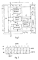
- the latch circuit 1 with their Function blocks 4, 5, 6, 7 up to the function block 7 usually an additional circuit of the Processor 2.
- MPCR Memory Protection Control Register
- the program flow in processor 2 is divided into command and data cycles.
- the CPU 2 fetches the next instruction to be executed from a program sequence, which is stored in the CPU or the memory device 3.
- the command cycle follows or several data cycles in which the CPU fetches or delivers data.
- Preferably be data is read from the memory device 3 and written back there, the reading and Writing locations can be assigned to different areas Bi of the storage device 3 can. Reading and writing can of course also start depending on the previous command other locations that can be addressed by the CPU.
- the data to be protected is only the data of the storage device 3.
- the storage device 3 can be divided into individual areas B0, B1, ..Bi, ..Bn or segments be treated differently with regard to an impermissible memory access from the outside are. So there can be first areas that neither read nor write, whereby the Term writing on overwriting with new data or on deleting related data. Reading data is permitted in the second area, but not but writing. The third area is data writing, but not reading authorized. And in fourth areas there is no restriction, so reading and writing is allowed in these storage areas without restriction. What protective function the individual Memory areas is in the memory protection register 7, which is also simplified below is referred to as MPCR. This memory protection register 7 is located as separate register e.g.
- the definition of the individual memory areas takes place in the address decoder 4, which from the supplied addresses A 0 ... A i ... A n, depending on the addressed memory area Bi, an area signal s2 (cf. for example the area signal CE memory i in FIG. 3) forms, the size of the memory areas is predetermined by the information of the area limits in the address decoder 4.
- the detection of whether there is a permissible or impermissible memory access takes place in the logical Linking device 5, the internal and external signals s2, s3, s4 and s1 logically with one another linked and recognizes permissible or impermissible access from the linking result.
- the basic access regulation for the addressed memory area Bi is from the Register 7 queried.
- the memory device 3 is read or written by the processor 2 by means of the control signals s3 or s5 emitted at the respective address A i , the data D 0 ... D n to be read or written, if appropriate, at the externally accessible data interface 6 can be read as data d1 or written from there to the memory device 3.
- the link device 5 between the CPU 2 and the memory device 3 is, as it were, transparent in this case and does not appear, although it links internal and external signals s2, s3, s4 and s1 to one another.
- the linking device 5 prevents reading or writing the memory device 3 required signals s5 or at least blocks the externally accessible data interface 6 via a blocking signal s6.
- the information about the The access device of the respective memory area asks the linking device 5 by means of of the area signal s2 serving as address from the register 7, which then the respective Access control reports back via signal s4.
- a basic condition for access security is that access to the memory device 3 by the processor 2 must not be hindered in normal operation.
- the CPU 2 runs through a complete command data cycle, in which the next command and thus program step is loaded into the CPU, which then sends the associated control command or commands, for example reading and / or writing, to the memory device 3 or others to be protected Triggers data sources or sinks.
- This regular operating cycle is identified, for example, by linking a status signal s3 with a range signal s2.
- An “op code fetch” signal “OPC”, which is logically linked to the area signal CE memory i is used, for example, as the status signal s3.
- the CPU generates the "op code fetch" signal whenever a command is accessed.
- An irregular memory access can also be characterized in that it contains certain contradictions between the signals s2, s3, s4. This is also checked.
- Various constellations between the signals and their effect on the access test are shown more clearly later by means of a table representation in FIG. 10.
- the MPCR register 7 in Fig. 3 contains 16 memory locations that are each in the "0" or "1" state and a total of one data word with 16 bit positions D0 to Correspond to D15. Assuming that the storage device 3 in eight different Memory areas B0 to B7 is divided, can thus be two from the 16-bit data word form separate 8-bit areas. An area defines the respective read access authorizations and the other the respective write access authorizations. With the first 8 bits for everyone of the 8 memory areas B0 to B7 a positive or negative read access authorization MRP0 to MRP7 and with the second 8 bits a positive or negative write access authorization MWP0 to MWP7 set. If the data volume in memory protection register 7 is less than 16 Bit are available, then the 16 access authorizations are separated into two Registers saved.
- the state "1" stored for the respective memory area Bi blocks access and State "0" enables it.
- the choice of which state in the MPCR register 7 the free access or the blocking defined is arbitrary in itself. However, it must be ensured that the unprogrammed State all bits of the MPCR register 7 have an enable state, otherwise it would a subsequent programming of the MPCR register and the memory device 3 is not more is possible. If through technology a certain state for the unprogrammed Register 7 is specified, then this state is possibly replaced by a subsequent one Inverter or corrected by reading the inverted register content.
- An address decoder 4 is shown schematically in FIG. 3. On the one hand there are the inputs for the address bits AD0 to ADn fed in parallel and on the other hand the decoding outputs which, depending on the decoded memory area B0 to Bn, each emit an area signal CE memory 0 to CE memory n .
- Possible ranges B0, B1, B2, Bn are given as a numerical example in hexadecimal format. For the uniqueness of the logic operation, it must be ensured that only one single area signal CE memory i is in state "1".
- FIG. 4 shows a block diagram similar to FIG. 1.
- a segmented memory type is used as the storage device 3, the individual areas Bi of which must be specifically controlled with an area read signal RE memory i or an area write signal WE memory i .
- a global memory release signal CE is required, which is present in parallel in all areas B0 to Bn.
- the area signal CE memory i from the address decoder 4 is fed to the link device 5.1, which combines this signal with the signals RE or WE originating from the CPU 2 and outputs it as the associated read area signal RE memory i or write area signal or WE memory i .
- This area can only be read or written if these signals match the corresponding memory area Bi. This is ensured by driving only a single area Bi with the read or write area signal.
- the other areas are not controlled.
- the read or write area signal is, of course, only issued if the access authorization check in the linkage device 5.1 uses the signals RE, WE, OPC, CE memory i , MRPQi or MWPQi and the signals TEST and JTAG, not shown, to determine permissible access. If access is not permitted, the signals RE memory i or WE memory i are suppressed by the link device 5.1.
- the global signal CE can, if necessary, be additionally suppressed by a suitable gate circuit.
- the block diagram of FIG. 5 contains a segmented memory device 3.
- the area selection is not carried out by an area read signal or an area write signal, but solely by the area signal CE memory i from the logic combination device 5.
- the read or write signal RE or WE of the CPU 2 is uniform for the entire memory device 3.
- an access check is carried out in the link device 5.2 via the existing signals. If access is recognized as inadmissible, the area signal CE memory i required for access in the memory device 3 is blocked.
- the global read or write signal RE or WE can optionally be additionally suppressed by a suitable gate circuit. This is not the case in FIG. 5, the signals RE, WE are therefore fed directly to the memory device 3, bypassing the logic device 5.2.
- FIG. 6 shows the logical combination device 5.1 of FIG. 4 more clearly for the reading case. So that the memory device 3 can be read by the CPU 2 in accordance with the read signal RE, the logic device must supply an area read signal RE memory i to the memory device in the event of a permissible memory access. From the memory protection register 7, only a single memory cell 10 is shown with the symbol of a D flip-flop. If the content MRPi of the memory cell 10 is to be changed, a new data bit Di is written into the memory cell 10 via the data line connected to the D input. A register write signal WE MPCR from the CPU 2 serves as the write clock .
- the memory protection register 7 is part of a flash memory, it must be taken into account that the unprogrammed memory state corresponds to the logic level "1". In order that this state is not interpreted as blocking information in the downstream linking device 5.1, the content MRPi of the memory cell 10 is read out inverted. In the D flip-flop 10 shown, this corresponds to a signal tap at the inverting output. A saved "1" thus becomes “0” and vice versa.
- a D flip-flop 11 is used to check whether there is a command access or data access to the memory device 3. It is clocked with the OP code fetch signal OPC at the C input and thus takes over the memory available at the D input. Release signal CE, if it exists.
- the output signal of this flip-flop 11 tapped off at the Q output is an auxiliary signal CEQ which has the state "1" until a new command access OPC is signaled without the memory release signal CE.
- the "1" state of the auxiliary signal CEQ thus signals that the last command access to the memory device 3 took place. In the "0" state, the auxiliary signal CEQ ultimately blocks the required area read signal RE memory i .
- the flip-flop 11 Via a reset input R, the flip-flop 11 can also be set to the "0" state by means of an internally or externally generated set reset signal S / R. This makes sense when the supply voltage is switched on because no memory access is to take place in this unstable operating state.
- a flip-flop with a “transparent latch” behavior is preferably used for the D flip-flop 11, so that during the starting process, as long as no clock signal OPC has yet been generated for the C input, the Q output is already present at the D input Memory release signal CE sees and can forward the subsequent AND gates 13, 14 as current information.
- the check as to whether the memory protection register 7 contains blocking or release information as content MRPi is carried out by a D flip-flop 12, the D input of which is connected to the data output of the memory cell 10.
- the valid information MRPi is adopted with a register write signal RE MPCR .
- RE MPCR register write signal
- the signal is emitted as signal MRPQi for further linking.
- the signal relates to the content of a single memory cell 10 and applies only to a single memory area Bi.
- the state "1" or "0" of this signal MRPQi corresponds to a blocking effect or a releasing effect.
- the blocking effect "1" is also forced via the set reset signal S / R at a set input S of the flip-flop 12 independently of other signals, for example when the network starts.
- the essential check as to whether there is an allowable or inadmissible memory access is carried out in two AND gates 13, 14 with multiple inputs. Some of these inputs, marked with small circles, invert the supplied signals before the AND operation.
- the first AND gate 13 is essentially responsible for those cases in which the content MRPi of the assigned memory cell 10 corresponds to release information. It then only has to be checked whether the addressed memory area CE memory i is also assigned to the addressed memory cell 10 and whether there is actually a read command RE from the CPU 2. If all three signals MRPQi, CEQ and RE have the correct state "0", "1", "1", then the area read signal RE memory is generated for the associated area Bi by means of an OR gate 15 connected downstream of the AND gate 13 i delivered.
- the second AND gate 14 is essentially responsible for those cases in which the content MRPi of the MPCR cell 10 corresponds to blocking information, ie in the flash example here has a "0". As above, it is also checked whether the addressed memory area CEi is also assigned to the addressed memory cell 10 and whether there is a read command RE generated by the CPU 2. If all conditions are met, this means that there is a permissible data access from the CPU 2 within a complete command and data cycle to the same memory area Bi. However, this only applies if no attempt is made to read the data using the external JTAG or TEST signals. Therefore, the absence of these signals is also included in the AND operation through gate 14. The negating inputs are used for this.
- the second AND gate 14 only outputs an area read signal RE memory i via the downstream OR gate 15 when the signals MRPQi, CEQ, RE, JTAG, TEST and CEi have the logic levels "1” , "1", “1", “0”, “0” and "1".
- the individual function blocks such as flip-flop stages, AND or OR gates are shown to understand the logical operations. These can of course be replaced in whole or in part by a corresponding other hardware or software, although the link can also be different if the result is identical.
- the above functional description of the link device 5.1 of FIG. 6 relates to the reading case. However, the same circuit applies to the write case, only some signals have to be replaced by the corresponding write signals. These signals MWPI, MWPQi, WE and WE memory i are shown in parentheses in the representation of the signals to be replaced.
- FIG. 7 shows, as an example, part of the logic device 5.2 from FIG. 5 as a block diagram with the individual logic units.
- the circuit shows the logic units and signals which are assigned to a single memory area Bi. The same arrangement is required for each memory area.
- the circuit supplies an area signal CE memory i when access to the memory device 3, not shown, is permitted.
- the linking device 5.2 is very similar to the described linking device 5.1 of FIG. 6 and contains two MPCR memory cells 20 and 21 for the read access information MRPi and the write access information MWRPi.
- the auxiliary signal CEQ is again formed by a "transparent" D flip-flop 22.
- the interrogation of the read access information from the cell 20 is carried out by a D flip-flop 23 and the write access information from the cell 21 is carried out by a D flip-flop 24, which deliver an MRPQ read or MWPQ write signal as output signals.
- the read access authorization is essentially determined by means of the two AND gates 25, 26 and the write access authorization is determined by means of the two AND gates 27, 28. All the AND gates of an area Bi are on the output side by means of an OR gate 29 merged, which emits an area signal CE memory i if at least one of the four AND gates has the logic state "1".
- the read or write operation can be differentiated using the read and write signals RE, WE. However, as in FIG. 7, both signals can also be combined as a single read / write signal R / W, where the logic level "0" means read and the logic level "1" means write.
- the AND gates 25, 26, 27, 28 each have at least three inputs, inverting inputs being marked with a small circle in FIG. 7.
- the linking device used here corresponds approximately to that Linking device 5.1 of FIG. 6 with released memory access.
- the first line shows a combined read / write signal R / W, which in the one logic state read and in the other writing means.
- the associated clocks T1, T2, T3 and T4 correspond to the equidistant areas of the R / W signal.
- the actual clock signal is not shown. Instead of the signals shown can of course, the inverted or inverse signals can also be used, provided the logic is adjusted accordingly.
- command access from the CPU 2 to the memory device 3 takes place. This corresponds to the OP code fetch signal OPC in line 2 and the memory area signal CE memory i in line 3.
- the command access is followed in the second cycle T2 by a read access to the same memory area Bi. This is signaled by the memory area signal CE memory i in cycle 2. An OPC signal is not generated because it is a data access.
- the data access belongs to a complete command data cycle in the same memory area Bi. This is indicated by the signal CEQ in the fourth line, which is set to the "1" state in the first cycle T1, and only again in the third cycle T3 by the new one OPC signal is reset.
- a new command data cycle begins in the third cycle T3, but does not extend to that previous memory area Bi, but to another memory area or another Data source or sink.
- the first four lines have nothing to do with a positive or negative access authorization, but with these signals R / W, OPC, CE memory i and CEQ the current status of the entire system is described.
- the read access authorization signal MRPQi for the area Bi specified In the fifth line is the read access authorization signal MRPQi for the area Bi specified. It has the logic level "0" during the entire time period and therefore means free read access to the memory area Bi.
- the sixth line shows the temporal course of the global read signal RE, which is always from the CPU 2 is activated when it queries commands or data from the memory device 3, that is during the first, second and fourth bars.
- the instruction call in the third cycle T3 does not solve any Read command RE off because the command data cycle started with the second OP code fetch signal does not access the memory device 3.
- the sixth line finally shows the resulting read area signal RE memory i , which is identical to the read signal RE except for a small time delay due to the signal delay by the logic switching stages, because a blocking effect for this memory area Bi is not provided for reading. So that the interdependency of the signals can be seen in the time diagram, FIGS. 8 and 9 contain arrows in the area of some signal changes in order to identify the triggering and resulting signal changes and signal states.
- the timing diagram of FIG. 9 is similar to the timing diagram of FIG. 8.
- the main difference consists in the read access authorization MRPQi in line 5 having the logical state "1" has and thus blocks the memory area Bi for unauthorized read access.
- the first and second clock T1, T2 comprise a regular command data cycle on the same memory area Bi.
- the reading process triggered by the CPU 2 in the first and second clock T1, T2 should, however, proceed unhindered despite the blocking information.
- the resulting read area signals RE memory i in the first and second clock are thus formed as in FIG. 8.
- the situation is different for the memory access attempt in the fourth clock T4.
- the fact that it is not a regular access results from the "0" level of the auxiliary signal CEQ.
- This signal in conjunction with the blocking signal MRPQi blocks the area read signal RE memory i , so that reading in the area Bi is not possible despite the correct area signal CE memory i .
- FIG. 10 shows in table form the mode of operation of the link device 5.1 from FIG. 6.
- the individual lines show the respective logic state with “0” and “1” of the signals indicated.
- the individual columns contain the following signals in succession: the area-related read access authorization MRPi, the JTAG signal, the TEST signal, the memory area signal CE memory i , the global read signal RE and finally the area read signal RE memory i.
- the last column shows the action resulting from the previous signals: "Read" or no read action.
- the read access authorization MRPQ i has the state "0" and this means that the associated memory area B i should not be blocked for reading, but rather allows free access.
- the status of the signals CEQ, JTAG and TEST is arbitrary for this access authorization.
- the linking device checks whether there is a contradiction between the area signal CE memory i and the global read signal RE. So line 1 is not read because the RE signal is inactive. Line 2 does not read because the area signal CE memory i is inactive. Only in the third line is the area signal and the global read signal set, so that the area read signal RE memory i is output with the state "1", and thus the memory device 3 is read at the addressed location.
- the logical combinations of lines 1, 2 and 3 take place in AND gate 13 according to FIG. 6.
- the auxiliary signal CEQ has the state "1" and therefore shows no contradiction to the total memory area B.
- read access is denied because the read signal RE is inactive.
- read access is denied because the area signal CE memory i is inactive.
- line 9 allows reading, even though memory area B i is blocked because processor 2 has regular memory access. However, as soon as unauthorized reading is attempted in this state via the JTAG or TEST signals, reading is prevented. These two signals must therefore be in the inactive state, which is identified here by "0". This can also be seen from lines 10 and 11, which prevent reading in the case of a locked memory area if one or both of these signals are active.
- the logical state of the other signals is arbitrary.
- the memory action shown in the table in the last column corresponds to the state of the area read signal RE memory i .
- the logical links of lines 4 to 11 can be realized by an AND link. This corresponds to the AND gate 14 of FIG. 6.
Landscapes
- Engineering & Computer Science (AREA)
- Theoretical Computer Science (AREA)
- Computer Security & Cryptography (AREA)
- Physics & Mathematics (AREA)
- General Engineering & Computer Science (AREA)
- General Physics & Mathematics (AREA)
- Storage Device Security (AREA)
Priority Applications (3)
| Application Number | Priority Date | Filing Date | Title |
|---|---|---|---|
| EP01108711A EP1248200A1 (fr) | 2001-04-06 | 2001-04-06 | Circuit de blocage pour empêcher un accès non autorisé à la mémoire d'un processeur |
| US10/117,975 US7054121B2 (en) | 2001-04-06 | 2002-04-08 | Protection circuit for preventing unauthorized access to the memory device of a processor |
| JP2002105364A JP2002358237A (ja) | 2001-04-06 | 2002-04-08 | プロセッサのメモリ装置に対する権限のないアクセスを防止する保護回路 |
Applications Claiming Priority (1)
| Application Number | Priority Date | Filing Date | Title |
|---|---|---|---|
| EP01108711A EP1248200A1 (fr) | 2001-04-06 | 2001-04-06 | Circuit de blocage pour empêcher un accès non autorisé à la mémoire d'un processeur |
Publications (1)
| Publication Number | Publication Date |
|---|---|
| EP1248200A1 true EP1248200A1 (fr) | 2002-10-09 |
Family
ID=8177073
Family Applications (1)
| Application Number | Title | Priority Date | Filing Date |
|---|---|---|---|
| EP01108711A Withdrawn EP1248200A1 (fr) | 2001-04-06 | 2001-04-06 | Circuit de blocage pour empêcher un accès non autorisé à la mémoire d'un processeur |
Country Status (3)
| Country | Link |
|---|---|
| US (1) | US7054121B2 (fr) |
| EP (1) | EP1248200A1 (fr) |
| JP (1) | JP2002358237A (fr) |
Families Citing this family (11)
| Publication number | Priority date | Publication date | Assignee | Title |
|---|---|---|---|---|
| US7185249B2 (en) * | 2002-04-30 | 2007-02-27 | Freescale Semiconductor, Inc. | Method and apparatus for secure scan testing |
| US7320642B2 (en) * | 2002-09-06 | 2008-01-22 | Wms Gaming Inc. | Security of gaming software |
| DE10347259B4 (de) * | 2003-10-08 | 2013-10-31 | Entropic Communications, Inc. | Verfahren zum Synchronisieren einer Schaltungsanordnung beim Empfang eines modulierten Signals |
| US7386774B1 (en) * | 2004-02-26 | 2008-06-10 | Integrated Device Technology, Inc. | Memory unit with controller managing memory access through JTAG and CPU interfaces |
| GB2442023B (en) * | 2006-09-13 | 2011-03-02 | Advanced Risc Mach Ltd | Memory access security management |
| JP5081761B2 (ja) * | 2008-08-05 | 2012-11-28 | 富士通株式会社 | アーカイブ装置,不正アクセス検出方法及び不正アクセス検出プログラム |
| CN103064798B (zh) * | 2011-10-19 | 2016-02-03 | 国基电子(上海)有限公司 | 电子设备 |
| TWI443518B (zh) | 2011-10-19 | 2014-07-01 | Hon Hai Prec Ind Co Ltd | 電子設備 |
| US10540524B2 (en) | 2014-12-31 | 2020-01-21 | Mcafee, Llc | Memory access protection using processor transactional memory support |
| WO2018230280A1 (fr) * | 2017-06-14 | 2018-12-20 | 住友電気工業株式会社 | Système de communication externe pour un véhicule, dispositif embarqué, procédé de commande de communication et programme de commande de communication |
| US20240086556A1 (en) | 2022-09-12 | 2024-03-14 | Idaho Scientific Llc | Computing data and instructions at immutable points |
Citations (5)
| Publication number | Priority date | Publication date | Assignee | Title |
|---|---|---|---|---|
| US4523271A (en) * | 1982-06-22 | 1985-06-11 | Levien Raphael L | Software protection method and apparatus |
| US4796235A (en) * | 1987-07-22 | 1989-01-03 | Motorola, Inc. | Write protect mechanism for non-volatile memory |
| US5557743A (en) * | 1994-04-05 | 1996-09-17 | Motorola, Inc. | Protection circuit for a microprocessor |
| US5657444A (en) * | 1995-08-03 | 1997-08-12 | National Semiconductor Corporation | Microprocessor with secure programmable read only memory circuit |
| US5974500A (en) * | 1997-11-14 | 1999-10-26 | Atmel Corporation | Memory device having programmable access protection and method of operating the same |
Family Cites Families (2)
| Publication number | Priority date | Publication date | Assignee | Title |
|---|---|---|---|---|
| US6397301B1 (en) * | 1999-12-29 | 2002-05-28 | Intel Corporation | Preventing access to secure area of a cache |
| US6665782B2 (en) * | 2001-08-16 | 2003-12-16 | International Business Machines Corporation | Method and apparatus for preventing unauthorized access of memory devices |
-
2001
- 2001-04-06 EP EP01108711A patent/EP1248200A1/fr not_active Withdrawn
-
2002
- 2002-04-08 US US10/117,975 patent/US7054121B2/en not_active Expired - Lifetime
- 2002-04-08 JP JP2002105364A patent/JP2002358237A/ja active Pending
Patent Citations (5)
| Publication number | Priority date | Publication date | Assignee | Title |
|---|---|---|---|---|
| US4523271A (en) * | 1982-06-22 | 1985-06-11 | Levien Raphael L | Software protection method and apparatus |
| US4796235A (en) * | 1987-07-22 | 1989-01-03 | Motorola, Inc. | Write protect mechanism for non-volatile memory |
| US5557743A (en) * | 1994-04-05 | 1996-09-17 | Motorola, Inc. | Protection circuit for a microprocessor |
| US5657444A (en) * | 1995-08-03 | 1997-08-12 | National Semiconductor Corporation | Microprocessor with secure programmable read only memory circuit |
| US5974500A (en) * | 1997-11-14 | 1999-10-26 | Atmel Corporation | Memory device having programmable access protection and method of operating the same |
Also Published As
| Publication number | Publication date |
|---|---|
| US7054121B2 (en) | 2006-05-30 |
| JP2002358237A (ja) | 2002-12-13 |
| US20020166034A1 (en) | 2002-11-07 |
Similar Documents
| Publication | Publication Date | Title |
|---|---|---|
| EP1276033B1 (fr) | Dispositif de mémoire ayant la protection de données dans un processeur | |
| DE2954731C2 (de) | Monolithischer Mikroprozessor | |
| DE3048365C2 (fr) | ||
| EP0128362B1 (fr) | Agencement de circuit comprenant une mémoire et une unité de contrôle d'accès | |
| EP1089219B1 (fr) | Méthode de proteger une mémoire de donnée | |
| EP0766211A2 (fr) | Carte à circuit intégré multifonctionnelle | |
| DE2749850B2 (de) | Hybrider Halbleiterspeicher mit assoziativer Seitenadressierung, Seitenaustausch und Steuerung auf dem Chip | |
| EP0224639B1 (fr) | Procédé pour contrôler l'accès à la mémoire d'une carte à circuit intégré et dispositif mettant en oeuvre ledit procédé | |
| EP1248200A1 (fr) | Circuit de blocage pour empêcher un accès non autorisé à la mémoire d'un processeur | |
| DE19963208B4 (de) | Verfahren zum Manipulationsnachweis einer programmierbaren Speichereinrichtung eines digitalen Steuergeräts | |
| EP1262856B1 (fr) | Unité contrôlée par programme | |
| DE102005022019A1 (de) | Sichere Verarbeitung von Daten | |
| EP0935214B1 (fr) | Carte à puce avec circuit intégré | |
| DE19954407A1 (de) | Verfahren zum direkten Aufrufen einer Funktion mittels eines Softwaremoduls durch einen Prozessor mit einer Memory-Management-Unit (MMU) | |
| DE1499742A1 (de) | Steuerbare Speicherzugriffsvorrichtung fuer Speichereinrichtungen von Datenverarbeitungsanlagen mit Multiprogrammverarbeitung | |
| DE19623145B4 (de) | Verfahren zum Betreiben eines Steuergerätes mit einer über eine Programmiervorrichtung programmierbaren Speichereinrichtung | |
| DE19901829A1 (de) | Schaltungsanordnung zur elektronischen Datenverarbeitung | |
| EP1563358B1 (fr) | Procede de controle securise d'une zone de memoire d'un microcontroleur faisant partie d'un dispositif de commande, et dispositif de commande pourvu d'un microcontroleur protege | |
| DE4227784A1 (de) | Rechnersystem und verfahren zum beheben eines seitenfehlers | |
| DE102021131424A1 (de) | Verfahren und systeme zur sitzungsbasierten und gesicherten zugriffsteuerung auf ein datenspeichersystem | |
| DE19612439C2 (de) | Halbleiterspeichervorrichtung | |
| EP0214390A1 (fr) | Procédé et dispositif pour libérer une mémoire utilisateur à accès contrôlé | |
| DE1524183C (fr) | ||
| DE10303452B4 (de) | Verfahren zur Steuerung der Unterbrechung und/oder der Aufzeichnung von Ausführungsdaten eines Programms in einem Mikrocontroller und Mikrocontroller mit einer Anordnung zur Durchführung des Verfahrens | |
| DE4340027A1 (de) | Schreibschutz-Verfahren für einen nichtflüchtigen Schreib-/Lesespeicher in einem elektronischen Steuergerät |
Legal Events
| Date | Code | Title | Description |
|---|---|---|---|
| PUAI | Public reference made under article 153(3) epc to a published international application that has entered the european phase |
Free format text: ORIGINAL CODE: 0009012 |
|
| AK | Designated contracting states |
Kind code of ref document: A1 Designated state(s): AT BE CH CY DE DK ES FI FR GB GR IE IT LI LU MC NL PT SE TR |
|
| AX | Request for extension of the european patent |
Free format text: AL;LT;LV;MK;RO;SI |
|
| 17P | Request for examination filed |
Effective date: 20030409 |
|
| AKX | Designation fees paid |
Designated state(s): DE FR GB IT NL |
|
| 17Q | First examination report despatched |
Effective date: 20060913 |
|
| 17Q | First examination report despatched |
Effective date: 20060913 |
|
| STAA | Information on the status of an ep patent application or granted ep patent |
Free format text: STATUS: THE APPLICATION IS DEEMED TO BE WITHDRAWN |
|
| 18D | Application deemed to be withdrawn |
Effective date: 20071023 |