EP1246265A2 - Light emitting device - Google Patents
Light emitting device Download PDFInfo
- Publication number
- EP1246265A2 EP1246265A2 EP02007028A EP02007028A EP1246265A2 EP 1246265 A2 EP1246265 A2 EP 1246265A2 EP 02007028 A EP02007028 A EP 02007028A EP 02007028 A EP02007028 A EP 02007028A EP 1246265 A2 EP1246265 A2 EP 1246265A2
- Authority
- EP
- European Patent Office
- Prior art keywords
- light emission
- light
- reflector
- substrate
- epitaxial
- Prior art date
- Legal status (The legal status is an assumption and is not a legal conclusion. Google has not performed a legal analysis and makes no representation as to the accuracy of the status listed.)
- Withdrawn
Links
Images






Classifications
-
- H—ELECTRICITY
- H10—SEMICONDUCTOR DEVICES; ELECTRIC SOLID-STATE DEVICES NOT OTHERWISE PROVIDED FOR
- H10H—INORGANIC LIGHT-EMITTING SEMICONDUCTOR DEVICES HAVING POTENTIAL BARRIERS
- H10H20/00—Individual inorganic light-emitting semiconductor devices having potential barriers, e.g. light-emitting diodes [LED]
- H10H20/80—Constructional details
- H10H20/81—Bodies
- H10H20/822—Materials of the light-emitting regions
- H10H20/823—Materials of the light-emitting regions comprising only Group II-VI materials, e.g. ZnO
-
- H—ELECTRICITY
- H10—SEMICONDUCTOR DEVICES; ELECTRIC SOLID-STATE DEVICES NOT OTHERWISE PROVIDED FOR
- H10H—INORGANIC LIGHT-EMITTING SEMICONDUCTOR DEVICES HAVING POTENTIAL BARRIERS
- H10H20/00—Individual inorganic light-emitting semiconductor devices having potential barriers, e.g. light-emitting diodes [LED]
- H10H20/80—Constructional details
- H10H20/85—Packages
- H10H20/852—Encapsulations
- H10H20/854—Encapsulations characterised by their material, e.g. epoxy or silicone resins
-
- H—ELECTRICITY
- H10—SEMICONDUCTOR DEVICES; ELECTRIC SOLID-STATE DEVICES NOT OTHERWISE PROVIDED FOR
- H10H—INORGANIC LIGHT-EMITTING SEMICONDUCTOR DEVICES HAVING POTENTIAL BARRIERS
- H10H20/00—Individual inorganic light-emitting semiconductor devices having potential barriers, e.g. light-emitting diodes [LED]
- H10H20/80—Constructional details
- H10H20/85—Packages
- H10H20/855—Optical field-shaping means, e.g. lenses
- H10H20/856—Reflecting means
-
- H—ELECTRICITY
- H10—SEMICONDUCTOR DEVICES; ELECTRIC SOLID-STATE DEVICES NOT OTHERWISE PROVIDED FOR
- H10H—INORGANIC LIGHT-EMITTING SEMICONDUCTOR DEVICES HAVING POTENTIAL BARRIERS
- H10H20/00—Individual inorganic light-emitting semiconductor devices having potential barriers, e.g. light-emitting diodes [LED]
- H10H20/80—Constructional details
- H10H20/882—Scattering means
-
- H—ELECTRICITY
- H10—SEMICONDUCTOR DEVICES; ELECTRIC SOLID-STATE DEVICES NOT OTHERWISE PROVIDED FOR
- H10W—GENERIC PACKAGES, INTERCONNECTIONS, CONNECTORS OR OTHER CONSTRUCTIONAL DETAILS OF DEVICES COVERED BY CLASS H10
- H10W72/00—Interconnections or connectors in packages
- H10W72/851—Dispositions of multiple connectors or interconnections
- H10W72/874—On different surfaces
- H10W72/884—Die-attach connectors and bond wires
-
- H—ELECTRICITY
- H10—SEMICONDUCTOR DEVICES; ELECTRIC SOLID-STATE DEVICES NOT OTHERWISE PROVIDED FOR
- H10W—GENERIC PACKAGES, INTERCONNECTIONS, CONNECTORS OR OTHER CONSTRUCTIONAL DETAILS OF DEVICES COVERED BY CLASS H10
- H10W74/00—Encapsulations, e.g. protective coatings
Definitions
- the present invention relates generally to light emitting devices in the form of a single semiconductor chip and capable of emitting light of white color, neutral colors between red and blue, i.e., magenta or pink and the like, and particularly to structures improving a spatial distribution of a color of light emitted thereby.
- LED high bright light emitting diode
- a device including a light emitting layer of AlGaAs, GaAsP and the like for red color has been put to practical use and an intensity of no less than several candela (Cd) has been implemented by an inexpensive LED.
- Cd candela
- Other than LEDs for red, GaP for green and yellow-green, GaInN for blue and green, AlGaInP for Mars yellow and yellow have all been put to practical use as inexpensive LEDs.
- LEDs all use a single semiconductor material for their light emitting layers and in principle they can only provide monochromatic light emission.
- typical LEDs are capable of emitting light of a primary color, a color between red and green, and a color between green and blue, such as red, Mars yellow, yellow, yellow-green, green, blue-green, blue, blue-violet and violet, they are incapable of emitting light of a neutral color between red and blue and a neutral color between red, green and blue.
- a source of light of a color between red and blue (e.g., magenta, pink), a color between red, blue and green (i.e., white), or the like is demanded, rather than a source of monochromatic light as described above.
- typical LEDs can only achieve a source of monochromatic light, and thus for their source of light a fluorescent lump, an incandescent lump or the like is used and it has thus suffered short lifetime, large sizes and low luminosity.
- the present inventors have succeeded in obtaining white light, pink light, magenta light and the like from a single LED using a ZnSe-based homoepitaxial layer formed on a ZnSe substrate, as has been described in Japanese Patent Laying-Open Nos. 2000-82845 and 2000-150960.
- a ZnSe substrate which is doped with iodine, aluminum, chlorine, bromine, gallium, indium or the like can provide conductance of n-type, and when it is illuminated with light of shorter than 510 nm, ZnSe can provide a so-called self-activated (SA) luminescence, a broad light emission having a center of an emission wavelength in a range of 550 nm to 650 nm. This light emission appears to be yellow, Mars yellow, or the like.
- SA self-activated
- the central wavelength and the half-width of emission spectrum of SA luminescence can be adjusted by the species, amount or the like of the dopant introduced.
- a light emission structure of ZnSe used as a matrix can be formed on a ZnSe substrate through homoepitaxy.
- ZnSe or ZnCdSe or ZnSeTe can be used for an active layer to form a high bright LED emitting light at a wavelength from 460 nm to 510 nm for blue color or blue-green color.
- Fig. 1 shows a concept of the present LED
- an epitaxial light emission structure provides blue or blue-green light emission, of which that emitted toward the substrate is absorbed by a ZnSe substrate 1 and excites optically SA light emission and thus provides yellow, Mars yellow or red light.
- the former light emission and the latter light emission can be combined together to obtain emission of light of white, pink, magenta or other similar neutral colors.
- the emitting point and the spatial distribution of the blue or blue-green emission at the epitaxial light emission structure are different from those of the yellow or Mars yellow light emission (that is, fluorescence) at the ZnSe substrate.
- the former light emission and the latter light emission are mixed at different ratios and the resultant light emission varies in color disadvantageously.
- the present LED is also be expected to be applied to displaying in mobile gear, such as a back light of a color liquid crystal display of a cellular phone, an illumination positioned under a key-button thereof, and the like significantly marketably.
- the present invention has been made to address the above issues.
- the present invention contemplates a light emitting device provided by a simple and inexpensive process, and emitting light of white, and magenta, pink and other similar neutral colors having a spatially uniform color distribution and provided in various color tones.
- the present light emitting device includes: a base having an electrode; a substrate formed of n-type ZnSe single crystal and mounted on the base; an epitaxial light emission structure comprised of a compound crystal relating ZnSe serving as a matrix thereof, the epitaxial light emission structure being provided on the substrate and emitting light when an electric current introduced thereinto; and a reflector correcting the difference in spatial distribution in intensity of light emission between the emitting light from the epitaxial structure and the fluorescence light from the substrate.
- the reflector scatters the fluorescence from the substrate in a direction of light emitted by the epitaxial light emitting structure. Furthermore the reflector is provided on the base located around the substrate.
- the reflector has an optical reflectance varying to adjust a ratio in intensity between the light emission from the epitaxial light emission structure and the fluorescence from the substrate. Two colors of light can thus be mixed at a ratio varying to obtain a mixture of colors in an aimed color tone as desired.
- the reflector includes resin of white color, resin having a light scattering medium buried therein, and resin having a surface covered with film of metal, and the base includes a printed circuit board formed of resin and having a patterned interconnection.
- the present light emitting device emits light of white color ranging from yellowish white color through bluish white color, or a neutral color including magenta, pink and the like.
- the present invention is applied to a light emission apparatus having a surface-mounted LED in a typical LED mounting system allowing an epitaxial light emission structure to face upward, or fixing a substrate to a base having an electrode and serving as a device frame, and it is importantly characterized in that the LED is surrounded by an optical reflector to reflect fluorescence provided from the ZnSe substrate in particular so as to provide a corrected spatial distribution in intensity of light emission.
- the present invention is applied to a bare chip of a multi-color LED having a substrate emitting light. As shown in Fig. 2, this bare chip provides a difference in a spatial distribution or directivity of light emission (E) between of the epitaxial light emission structure and of fluorescent light emission (S) from the substrate.
- E light emission
- S fluorescent light emission
- the light emission from the epitaxial layer is that from a significantly thin layer of an outermost surface of the bare chip, whereas the fluorescence from the substrate is light emission from the entire chip, i.e., there is a difference in position between the former light emission and the latter light emission.
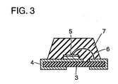
- a typical, surface-mounted LED mounting method, or molding is employed, e.g., as shown in Fig. 3, an LED (or chip) 5 mounted on a resin base 3 having a patterned interconnection 4 is sealed with transparent resin 7, then the mounted LED 5 provides light emission having a spatial distribution in intensity similar to that of the bare chip.
- the two light emissions are mixed at different ratios and color tone cannot spatially be uniform.
- fluorescence emitted from ZnSe substrate 1 in particular has its spatial distribution in intensity changed by a reflector external to LED 5 to be close to that in intensity of light emission from epitaxial light emission structure 2.
- fluorescence from ZnSe substrate 1 that radiates to a direction parallel to a surface on which LED 5 is mounted is reflected by a reflector 8 formed on resin base 3 to allow the light to radiate to a direction perpendicular to the surface having LED 5 mounted thereon.
- the spatial distribution in intensity of fluorescence of ZnSe substrate 1 can be changed to be biased in a direction perpendicular to the surface having LED 5 mounted thereon.
- the spatial distribution of light emission of epitaxial light emission structure 2 is originally biased in a direction perpendicular to the surface having LED 5 mounted thereon, and the spatial distribution in intensity of fluorescence of ZnSe substrate 1 can thus be matched to that in intensity of light emission of epitaxial light emission structure 2.
- Possible reflector 8 in effect used is that having an arc-shaped surface, a parabolic-shaped surface or the like, or a flat surface or the like. Furthermore, possible such surfaces include a mirror-finished surface, a rough surface introducing diffusion, or the like. With its positional relationship with LED 5 taking into consideration, the Fig. 4A structure is readily be designed.
- Reflector 8 can be formed of a highly reflective metal (e.g., a gold-plated copper plate), white resin (e.g., liquid crystal polymer-based resin), resin having a light scattering medium (e.g., titania, silica) distributed to provide an increased optical reflectance, resin having a surface covered with film of metal, or the like.
- a highly reflective metal e.g., a gold-plated copper plate
- white resin e.g., liquid crystal polymer-based resin
- resin having a light scattering medium e.g., titania, silica
- Surface-mounted LED 5 having reflector 8 is similar in geometry to a so-called reflector-type package in a package of a typical, monocolor LED using GaP or the like.
- typical reflector-type packages are contemplated mainly to change light emission in directivity to collect light emitted by LED 5 and thus increase the luminosity of LED 5 in an exactly upward direction.
- Figs. 4C and 4D show an exemplary structure of the aforementioned reflector-type package.
- a reflector 9 had been intended to increase luminosity. More specifically it had been intended to reflect upwards the light radiating in a direction parallel to a surface having LED 5a mounted thereon.
- reflector 9 adopted had often been that significantly inclined in angle, a paraboloid capable of collimating light received from a point source of light, or the like.
- the present invention is distinguished therefrom and contemplates generally matching the spatial distributions in intensity of two light emissions different in directivity, as described above, to emit uniform, mixed-color light. Accordingly, reflector 8 for mixing colors has an optimal structure different from that of typical reflector 9.
- color mixing reflector 8 has a reflecting surface, as optimized in structure, including for example an arc reflecting plane, a flat reflecting plane forming an angle of 40° to 90° with a plane having LED 5 mounted thereon, and the like. Furthermore, the reflector is widely ranged from a metallic reflecting surface having a reflectance exceeding 90% to a tinted resin surface having a reflectance of only approximately 10%.
- LED 5 of the present invention is characterized in changing the ratio in intensity between light emission from epitaxial light emission structure 2 and fluorescence from ZnSe substrate 1 to adjust the color of the mixture thereof, i.e., the color of light emitted by the LED.
- epitaxial light emission structure 2 is a structure having a sharp light emission peak at 485 nm and the substrate is ZnSe 1 doped with iodine (I), then the substrate's fluorescence would be light emission having a broad peak with 585 nm.
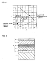
- Epitaxial light emission structure 2 provides light emission (blue light emission) indicated by a black square and ZnSe substrate 1 allows fluorescence (yellow light emission) indicated by a black circle and the colors that are mixed together are represented by a point on a line connecting the two points.
- a bluish white color i.e., a cold white color would be provided, as represented by a point A,.
- a yellowish white color i.e., a warm white color would be provided, as represented by a point C.
- pure white color would be provided, as represented by a point B.
- Emission of fluorescence of ZnSe substrate 1 can be adjusted in intensity not only by changing the original luminosity of the substrate, as described above, but also changing the efficiency in externally extracting the fluorescence of the substrate.
- the latter technique can also be as effective as described above.
- reflector 8 having a low optical reflectance results in a reduced amount of the fluorescence of ZnSe substrate 1 that is reflected in a direction perpendicular to a surface having LED 5 mounted thereon.
- This can implement a color tone with epitaxial light emission larger in proportion. (For an LED for white color, a bluish white color can be provided.)
- reflector 8 having a high optical reflectance results in fluorescence of ZnSe substrate 1 having a large portion reflected in a direction perpendicular to the surface having LED 5 mounted thereon.
- This can implement a color tone with the substrate's fluorescence larger in proportion (For an LED for white color, a yellowish white color can be provided.).
- a color tone as desired e.g., pure white color
- the resultant mixture of light emitted can also have a spatially uniform distribution.
- LED 5 does not have any difference from a conventional, surface-mounted LED chip in geometry and how it is fabricated, and it is not necessary to adopt a mounting structure having an epitaxial layer facing downward, an embedded structure, or the like. As such, an already established, inexpensive technique of fabricating a surface-mounted LED can exactly be applied in the present invention.
- a surface-mounted LED which emits light in any direction in a uniform tone, allows emitted light to appear to have a single tone in whichever direction it may be seen, and provides light of white, and magenta, pink and other similar neutral colors in a variety of color tones
- an epitaxial light emission structure 2 as shown in Fig. 6, for blue color having a peaked emission wavelength of 485 nm is grown by homoepitaxy with an MBE method.
- Epitaxial light emission structure 2 is composed of a p-type contact layer 14 having a superlattice structure of a stack of layers of ZnTe and , ZnSe doped to be p-type, a p-type clad layer 13 formed of a layer of Zn 0.85 Mg 0.15 S 0.10 Se 0.90 doped to be p-type, a single quantum well active layer 12 formed of a structure of a stack of layers of a ZnSe layer and a Zn 0.88 Cd 0.12 Se layer, an n-type clad layer 11 formed of a Zn 0.85 Mg 0.15 S 0.10 Se 0.90 layer doped to be n type, and an n-type ZnSe buffer layer 10.
- a patterned, p-type electrode formed of Ti/Au in a lattice there is formed a full-surface covered Au electrode in a thin film of no more than 20 nm in thickness, and on the substrate at a back surface thereof an n-type electrode formed of In is provided.
- the epitaxial wafer is cut to be a chip (of type 1) sized to be 400 ⁇ m x 400 ⁇ m and having a thickness of 200 ⁇ m. Furthermore, exactly the same procedure is used to form on an Al-doped ZnSe substrate 1 a structure for blue color having a peaked emission wavelength of 475 nm and cut the resultant product in the form of a chip.
- a device A is a simple, flat reflector 8, with a reflecting surface 8a and a surface having LED 5 mounted thereon together forming an angle of 70°.
- a device B is a similarly flat reflector 8, with reflecting surface 8a and the surface having LED 5 mounted thereon together forming an angle of 40°.
- a device C is a reflector 8 having an arc, reflecting surface 8a having a center at the position of an opening located exactly above LED 5.
- a device D is reflector 8 having a parabolic reflecting plane 8a with a focus corresponding to the position at which LED 5 is mounted.
- Reflector 8 has an opening with an upper end sized to be 1.2 mm and a height of 0.8 mm. Furthermore in the present embodiment on the side of a surface having LED 5 mounted thereon reflector 8 has an opening shaped to be a square.
- Reflector 8 is formed of a white, liquid crystal polymer-based resin, and a base with an electrode is a printed circuit board (resin base 3) formed of BT resin with a patterned interconnection 4 of a structure of a stack of layers Cu/Ni/Au provided thereto.
- the printed circuit board and reflector 8 are stuck together with adhesive to fabricate LED 5. Since it is a surface-mounted device, patterned interconnection 4 extends to a back surface of the device (or a back surface of the printed circuit board).
- white resin is insert-molded and thus formed in a reflector on a lead frame for example of copper- or iron-based metal.
- reflector 8 has an opening sealed with transparent resin (epoxy resin) 7.
- epitaxial light emission structure 2 provided blue light emission having a peak of 485 nm and furthermore the blue light emission was partially absorbed by ZnSe substrate 1 and through fluorescence the substrate emitted yellow fluorescence having a peak of 585 nm.
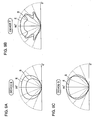
- the blue light emission and the yellow fluorescence are specially distributed, as shown in Figs, 8A-8D for devices A-D, respectively.
- reflector 8 reflects the substrate's fluorescence that radiates in a direction parallel to a surface having LED 5 mounted thereon and thus redirects it to radiate in a direction perpendicular to the surface having LED 5 mounted thereon, to allow fluorescence to significantly vary in directivity.
- the light emission from the epitaxial structure 2 inherently does not have a high intensity in the direction of reflector 8, and thus the spatial distribution is not significantly changed.
- the spatial distribution in intensity of light from epitaxial structure 2 and that in intensity of light from substrate 1 substantially match and as a result there has been obtained LED 5 allowing a constant color tone in whichever direction it is observed.
- device D of parabolic type is most inferior in that the epitaxial structure 2 light emission and the substrate's fluorescence least match in directivity, and the problem of mottling is not completely resolved, although the device is brightest in terms of the intensity in an exactly upward direction.
- color mixing reflector 8 has an opening shaped to be a square
- the present invention is similarly effective if reflector 8 has an opening shaped for example in a circle or a rectangle.
- the opening is square, rectangular or the like
- a reflector with a pair of color mixing reflectors 8 having a geometry as seen in a direction and that of color mixing reflectors 8 having a different geometry as seen in a direction perpendicular thereto e.g., a color mixing reflector having a cross section of device A in a direction and a cross section of device B in a direction perpendicular thereto
- the present invention in a second embodiment will now be described.
- a chip similar to the chip of type 1 used in the first embodiment was prepared.
- the chip was also mounted in a structure having a reflector having the geometry of device A used in the first embodiment. It should be noted, however, that herein reflector 8 is formed of different material and has a surface in a different condition than the first embodiment.
- a reflector is formed of opaque resin containing titania diffused therein
- a smooth surface of resin plated with gold to provide a mirror finished surface is employed for reflector 8
- a surface of resin having small protrusions and depressions and plated with silver to be moderately glossy is used for reflector 8. They are mounted, as has been described in the first embodiment.
- LED 5 fabricated in the present embodiment provides a distribution of in intensity blue light emission from epitaxial light emission structure 2 and that in intensity of yellow fluorescence from ZnSe substrate 1, as represented in Figs. 9A-9C.
- devices E and G allowed the blue light emission and the yellow fluorescence to substantially match in directivity and were thus able to provide LED 5 emitting light spatially uniform in color.
- device G allows the substrate providing fluorescence radiated with a grater intensity than device E and this means that reflector 8 plated with gold has a higher reflectance. Consequently, device G provided white color more yellowish in color tone than device E. It should be noted that device E provided a correlated color temperature of 4500K and device G provided that of 3700K.
- the substrate provides fluorescence having a spatial profile having protrusions. This is because reflector 8 has reflecting surface 8a mirror finished and there thus appeared a directivity reflecting a light emission point of LED 5.
- reflector 8 preferably has reflecting surface 8a roughened (or having protrusions and depressions) to introduce diffusion.
- a reflector is formed of a less reflective, yellow, liquid crystal polymer-based resin and the reflector, with reflecting surface 8a and an LED 5 mounted surface forming an angle of 80°
- a reflector is formed of a less reflective, brown, liquid crystal polymer-based resin and reflector 8 and an LED 5 mounted surface form an angle of 90°. They were mounted, as has been described in the first embodiment.
- LED 5 fabricated in the present embodiment provided a spatial emission distribution in intensity of blue light emission from epitaxial light emission structure 2 and that in intensity of yellow fluorescence from ZnSe substrate 1, as shown in Figs. 11A and 11B.
- devices H and I both allow the blue light emission and the yellow fluorescence to substantially match in directivity and were able to provide LED 5 emitting light spatially uniform in color.
- the substrate provides fluorescence radiated with a smaller intensity than for example in device A of the first embodiment and device E of the second embodiment. This is attributed to the fact that reflector 8 is smaller in reflectance than the material described above.
- device H with the chip of type 1 mounted therein provided substantially pure white color and device I with the chip of type 1 mounted therein provided white color bluish in color tone.
- device H provided a correlated color temperature of 6000K and device I provided that of 10000K.
- device H with the chip of type 2 mounted thereon and device I with the chip of type 2 mounted therein were able to emit light of pink color and that of violet color, respectively, both uniform spatially.
- a reflector can be provided and a spatial distribution in intensity of fluorescence from a substrate can thus approximate to that in intensity of light emission from an epitaxial light emission structure.
- a light emitting device emitting light in any direction in a uniform color tone and allowing light emission to appear to have a single color tone in whichever direction the light may be observed.
- the substrate having the epitaxial light emission structure can be mounted on a base having an electrode and an already established, inexpensive surface-mounted LED fabrication technology can thus be applied as it is.
- an inexpensive and simple process can be used to fabricate the light emitting device.
- a light emitting device providing white, magenta, pink and other similar neutral colors in various color tones that emit light having a spatially uniform distribution in color can inexpensively and readily be fabricated and is expected to be significantly demanded for applications such as displaying in mobile gear, liquid crystal display's backlight, decoration and the like in particular.
Landscapes
- Led Device Packages (AREA)
- Led Devices (AREA)
Abstract
Description
Claims (6)
- A light emitting device comprising:a base (3) having an electrode (4);a substrate (1) formed of n-type ZnSe single crystal and mounted on said base;an epitaxial light emission structure (2) formed of a compound crystal relating ZnSe serving as a matrix thereof, said epitaxial light emission structure being provided on said substrate and emitting light when an electric current introduced thereinto; anda reflector (1) matching a spatial distribution in intensity of light emission from said epitaxial light emission structure to a spatial distribution in intensity of fluorescence obtained in said substrate excited with the light emission from said epitaxial light emission structure.
- The light emitting device of claim 1, wherein said reflector scatters said fluorescence from said substrate in a direction of light emitted by said light emitting device.
- The light emitting device of claim 1, wherein said reflector is provided on said base located around said substrate.
- The light emitting device of claim 1, wherein said reflector has an optical reflectance varying to adjust a ratio in intensity between said light emission from the said epitaxial light emission structure and said fluorescence from said substrate.
- The light emitting device of claim 1, wherein:said reflector includes resin of white color, resin having a light scattering medium buried therein, or resin having a surface covered with film of metal; andsaid base includes a printed circuit board formed of resin and having a patterned interconnection (4).
- The light emitting device of claim 1, emitting light of white color ranging from yellowish white color through bluish white color, or a neutral color including magenta, pink and the like.
Applications Claiming Priority (2)
| Application Number | Priority Date | Filing Date | Title |
|---|---|---|---|
| JP2001097844 | 2001-03-30 | ||
| JP2001097844A JP2002299698A (en) | 2001-03-30 | 2001-03-30 | Light emitting device |
Publications (2)
| Publication Number | Publication Date |
|---|---|
| EP1246265A2 true EP1246265A2 (en) | 2002-10-02 |
| EP1246265A3 EP1246265A3 (en) | 2007-09-05 |
Family
ID=18951573
Family Applications (1)
| Application Number | Title | Priority Date | Filing Date |
|---|---|---|---|
| EP02007028A Withdrawn EP1246265A3 (en) | 2001-03-30 | 2002-03-27 | Light emitting device |
Country Status (5)
| Country | Link |
|---|---|
| US (1) | US6642547B2 (en) |
| EP (1) | EP1246265A3 (en) |
| JP (1) | JP2002299698A (en) |
| KR (1) | KR100576892B1 (en) |
| TW (1) | TW560086B (en) |
Cited By (9)
| Publication number | Priority date | Publication date | Assignee | Title |
|---|---|---|---|---|
| WO2005093862A3 (en) * | 2004-03-26 | 2006-04-27 | Matsushita Electric Industrial Co Ltd | Led mounting module, led module, manufacturing method of led mounting module, and manufacturing method of led module |
| EP1440481B1 (en) * | 2001-10-31 | 2007-09-19 | Osram Opto Semiconductors GmbH | Optoelectronic component |
| CN100414701C (en) * | 2006-06-08 | 2008-08-27 | 弘元科技有限公司 | Light emitting system, light emitting device and forming method thereof |
| WO2008089165A3 (en) * | 2007-01-19 | 2008-12-18 | Cree Inc | High performance led package |
| EP1598590A3 (en) * | 2003-12-30 | 2010-01-06 | OSRAM Opto Semiconductors GmbH | Illumination device with optimized light extracting surface |
| EP1521313A3 (en) * | 2003-10-03 | 2010-12-29 | Philips Lumileds Lighting Company LLC | Integrated reflector cup for a light emitting device mount |
| RU2466481C1 (en) * | 2011-05-05 | 2012-11-10 | Открытое акционерное общество "Научно-исследовательский институт полупроводниковых приборов" (ОАО "НИИПП") | Semiconductor radiation source |
| EP2284914B1 (en) * | 2002-12-06 | 2016-04-20 | Cree, Inc. | LED package comprising leadframe and two-part heatsink |
| EP2859596B1 (en) * | 2012-06-11 | 2020-08-12 | Cree, Inc. | Led package with encapsulant having planar surfaces |
Families Citing this family (65)
| Publication number | Priority date | Publication date | Assignee | Title |
|---|---|---|---|---|
| WO2000079605A1 (en) * | 1999-06-23 | 2000-12-28 | Citizen Electronics Co., Ltd. | Light emitting diode |
| US7112916B2 (en) * | 2002-10-09 | 2006-09-26 | Kee Siang Goh | Light emitting diode based light source emitting collimated light |
| TW560697U (en) * | 2002-11-26 | 2003-11-01 | Topson Technology Co Ltd | Surface-mounting type light-emitting diode structure |
| CN1297017C (en) * | 2003-01-28 | 2007-01-24 | 诠兴开发科技股份有限公司 | pink light emitting diode |
| JP4254266B2 (en) | 2003-02-20 | 2009-04-15 | 豊田合成株式会社 | LIGHT EMITTING DEVICE AND LIGHT EMITTING DEVICE MANUFACTURING METHOD |
| CN102290409B (en) * | 2003-04-01 | 2014-01-15 | 夏普株式会社 | Light-emitting apparatus |
| KR20040092512A (en) * | 2003-04-24 | 2004-11-04 | (주)그래픽테크노재팬 | A semiconductor light emitting device with reflectors having a cooling function |
| US6864513B2 (en) * | 2003-05-07 | 2005-03-08 | Kaylu Industrial Corporation | Light emitting diode bulb having high heat dissipating efficiency |
| US7108386B2 (en) * | 2003-05-12 | 2006-09-19 | Illumitech Inc. | High-brightness LED-phosphor coupling |
| AT501081B8 (en) * | 2003-07-11 | 2007-02-15 | Tridonic Optoelectronics Gmbh | LED AS WELL AS LED LIGHT SOURCE |
| US7145182B2 (en) * | 2003-09-12 | 2006-12-05 | Avago Technologies General Ip (Singapore) Pte. Ltd. | Integrated emitter devices having beam divergence reducing encapsulation layer |
| JP2005091675A (en) * | 2003-09-17 | 2005-04-07 | Pentax Corp | Light emitting device |
| US20050077535A1 (en) * | 2003-10-08 | 2005-04-14 | Joinscan Electronics Co., Ltd | LED and its manufacturing process |
| JP4934944B2 (en) * | 2003-11-04 | 2012-05-23 | 日亜化学工業株式会社 | Manufacturing method of semiconductor light emitting device |
| US20050156510A1 (en) * | 2004-01-21 | 2005-07-21 | Chua Janet B.Y. | Device and method for emitting output light using group IIB element selenide-based and group IIA element gallium sulfide-based phosphor materials |
| US20050167684A1 (en) * | 2004-01-21 | 2005-08-04 | Chua Janet B.Y. | Device and method for emitting output light using group IIB element selenide-based phosphor material |
| DE202005002110U1 (en) * | 2004-02-19 | 2005-05-04 | Hong-Yuan Technology Co., Ltd., Yonghe | Light-emitting device |
| JP2005321693A (en) * | 2004-05-11 | 2005-11-17 | Hitachi Displays Ltd | Liquid crystal display |
| JP2006005290A (en) * | 2004-06-21 | 2006-01-05 | Citizen Electronics Co Ltd | Light emitting diode |
| DE102004045947A1 (en) * | 2004-06-30 | 2006-01-19 | Osram Opto Semiconductors Gmbh | LED array |
| DE102004045950A1 (en) * | 2004-09-22 | 2006-03-30 | Osram Opto Semiconductors Gmbh | Housing for an optoelectronic component, optoelectronic component and method for producing an optoelectronic component |
| WO2006090834A1 (en) * | 2005-02-24 | 2006-08-31 | Kyocera Corporation | Light emitting device and lighting apparatus |
| US7381995B2 (en) * | 2005-03-16 | 2008-06-03 | Industrial Technology Research Institute | Lighting device with flipped side-structure of LEDs |
| JP2006351882A (en) * | 2005-06-16 | 2006-12-28 | Rohm Co Ltd | Optical semiconductor device |
| JP4739842B2 (en) * | 2005-07-25 | 2011-08-03 | スタンレー電気株式会社 | Surface mount type LED |
| US20070034886A1 (en) * | 2005-08-11 | 2007-02-15 | Wong Boon S | PLCC package with integrated lens and method for making the package |
| JP4715422B2 (en) * | 2005-09-27 | 2011-07-06 | 日亜化学工業株式会社 | Light emitting device |
| WO2007058514A1 (en) | 2005-11-21 | 2007-05-24 | Seoul Semiconductor Co., Ltd. | Light emitting element |
| US8039849B2 (en) * | 2005-11-23 | 2011-10-18 | Taiwan Oasis Technology Co., Ltd. | LED module |
| JP5082427B2 (en) * | 2005-12-26 | 2012-11-28 | 東芝ライテック株式会社 | Light emitting device |
| WO2012135976A1 (en) * | 2011-04-07 | 2012-10-11 | Cree Huizhou Solid State Lighting Company Limited | Led device having tilted peak emission and led display including such devices |
| US11210971B2 (en) * | 2009-07-06 | 2021-12-28 | Cree Huizhou Solid State Lighting Company Limited | Light emitting diode display with tilted peak emission pattern |
| KR100820529B1 (en) | 2006-05-11 | 2008-04-08 | 엘지이노텍 주식회사 | Light emitting device and manufacturing method thereof, surface light emitting device |
| WO2007140651A1 (en) * | 2006-06-08 | 2007-12-13 | Hong-Yuan Technology Co., Ltd | Light emitting system, light emitting apparatus and forming method thereof |
| US20080048199A1 (en) * | 2006-08-24 | 2008-02-28 | Kee Yean Ng | Light emitting device and method of making the device |
| US7910938B2 (en) * | 2006-09-01 | 2011-03-22 | Cree, Inc. | Encapsulant profile for light emitting diodes |
| KR100859496B1 (en) * | 2006-11-07 | 2008-09-22 | 한국에너지기술연구원 | LED lamp manufacturing method |
| US20080175009A1 (en) * | 2007-01-19 | 2008-07-24 | Unity Opto Technology Co., Ltd. | Edge-emitting light-emitting diode |
| KR100901618B1 (en) | 2007-04-19 | 2009-06-08 | 엘지이노텍 주식회사 | Light emitting diode package and manufacturing method |
| TWI346514B (en) * | 2007-06-05 | 2011-08-01 | Young Lighting Technology Corp | Back light module and light emitting diode package structure therefor |
| US20090032827A1 (en) * | 2007-07-30 | 2009-02-05 | Philips Lumileds Lighting Company, Llc | Concave Wide Emitting Lens for LED Useful for Backlighting |
| KR101283054B1 (en) * | 2007-08-20 | 2013-07-05 | 엘지이노텍 주식회사 | Light emitting device |
| PL3051586T3 (en) * | 2007-10-09 | 2018-08-31 | Philips Lighting North America Corporation | Integrated led-based luminaire for general lighting |
| US8129735B2 (en) * | 2008-09-24 | 2012-03-06 | Koninklijke Philips Electronics N.V. | LED with controlled angular non-uniformity |
| TWI411142B (en) * | 2009-06-23 | 2013-10-01 | 台達電子工業股份有限公司 | Light emitting device and packaging method thereof |
| TWI394298B (en) * | 2010-01-29 | 2013-04-21 | 榮創能源科技股份有限公司 | Semiconductor light emitting device package structure |
| US8350370B2 (en) * | 2010-01-29 | 2013-01-08 | Cree Huizhou Opto Limited | Wide angle oval light emitting diode package |
| KR100969100B1 (en) | 2010-02-12 | 2010-07-09 | 엘지이노텍 주식회사 | Light emitting device, manufacturing method and light emitting device package |
| JP5786278B2 (en) * | 2010-04-07 | 2015-09-30 | 日亜化学工業株式会社 | Light emitting device |
| US8723409B2 (en) | 2010-04-07 | 2014-05-13 | Nichia Corporation | Light emitting device |
| US20120161170A1 (en) * | 2010-12-27 | 2012-06-28 | GE Lighting Solutions, LLC | Generation of radiation conducive to plant growth using a combination of leds and phosphors |
| US10147853B2 (en) | 2011-03-18 | 2018-12-04 | Cree, Inc. | Encapsulant with index matched thixotropic agent |
| JP2013138099A (en) * | 2011-12-28 | 2013-07-11 | Iwasaki Electric Co Ltd | Led module |
| US10468565B2 (en) | 2012-06-11 | 2019-11-05 | Cree, Inc. | LED package with multiple element light source and encapsulant having curved and/or planar surfaces |
| US10424702B2 (en) | 2012-06-11 | 2019-09-24 | Cree, Inc. | Compact LED package with reflectivity layer |
| US9887327B2 (en) | 2012-06-11 | 2018-02-06 | Cree, Inc. | LED package with encapsulant having curved and planar surfaces |
| JP2014041993A (en) * | 2012-07-24 | 2014-03-06 | Toyoda Gosei Co Ltd | Light-emitting device and method of manufacturing the same |
| US9461024B2 (en) | 2013-08-01 | 2016-10-04 | Cree, Inc. | Light emitter devices and methods for light emitting diode (LED) chips |
| USD758976S1 (en) | 2013-08-08 | 2016-06-14 | Cree, Inc. | LED package |
| WO2015101899A1 (en) | 2014-01-06 | 2015-07-09 | Koninklijke Philips N.V. | Thin led flash for camera |
| USD790486S1 (en) | 2014-09-30 | 2017-06-27 | Cree, Inc. | LED package with truncated encapsulant |
| USD777122S1 (en) | 2015-02-27 | 2017-01-24 | Cree, Inc. | LED package |
| USD783547S1 (en) | 2015-06-04 | 2017-04-11 | Cree, Inc. | LED package |
| WO2017164644A1 (en) * | 2016-03-22 | 2017-09-28 | 엘지이노텍 주식회사 | Light-emitting device and light-emitting module having same |
| US20170372646A1 (en) * | 2016-06-23 | 2017-12-28 | Nanolumens Acquisition, Inc. | Display System and Apparatus with Directional Emission |
Family Cites Families (25)
| Publication number | Priority date | Publication date | Assignee | Title |
|---|---|---|---|---|
| US5198690A (en) * | 1990-11-26 | 1993-03-30 | Sharp Kabushiki Kaisha | Electroluminescent device of II-IV compound semiconductor |
| JPH06237047A (en) * | 1993-02-10 | 1994-08-23 | Sony Corp | Semiconductor light-emitting element |
| JP3329573B2 (en) * | 1994-04-18 | 2002-09-30 | 日亜化学工業株式会社 | LED display |
| DE19638667C2 (en) * | 1996-09-20 | 2001-05-17 | Osram Opto Semiconductors Gmbh | Mixed-color light-emitting semiconductor component with luminescence conversion element |
| JP3504079B2 (en) * | 1996-08-31 | 2004-03-08 | 株式会社東芝 | Method for manufacturing semiconductor light emitting diode device |
| JPH10190064A (en) * | 1996-12-24 | 1998-07-21 | Nichia Chem Ind Ltd | Light emitting diode and LED display using the same |
| US6274890B1 (en) * | 1997-01-15 | 2001-08-14 | Kabushiki Kaisha Toshiba | Semiconductor light emitting device and its manufacturing method |
| EP1959506A2 (en) * | 1997-01-31 | 2008-08-20 | Matsushita Electric Industrial Co., Ltd. | Method of manufacturing a semiconductor light-emitting device |
| JPH10284757A (en) * | 1997-04-04 | 1998-10-23 | Toyoda Gosei Co Ltd | Light emitting diode device |
| JPH1187778A (en) * | 1997-09-02 | 1999-03-30 | Toshiba Corp | Semiconductor light emitting element, semiconductor light emitting device and method for manufacturing the same |
| US6340824B1 (en) * | 1997-09-01 | 2002-01-22 | Kabushiki Kaisha Toshiba | Semiconductor light emitting device including a fluorescent material |
| JP3704941B2 (en) * | 1998-03-30 | 2005-10-12 | 日亜化学工業株式会社 | Light emitting device |
| JP3087742B2 (en) * | 1998-07-09 | 2000-09-11 | 住友電気工業株式会社 | White LED |
| JP3087743B2 (en) * | 1998-11-12 | 2000-09-11 | 住友電気工業株式会社 | Intermediate color LED |
| TW406442B (en) * | 1998-07-09 | 2000-09-21 | Sumitomo Electric Industries | White colored LED and intermediate colored LED |
| JP4348488B2 (en) * | 1998-11-13 | 2009-10-21 | 住友電気工業株式会社 | LED substrate |
| KR100545441B1 (en) * | 1998-07-28 | 2006-01-24 | 스미토모덴키고교가부시키가이샤 | LED Substrate |
| JP3785820B2 (en) * | 1998-08-03 | 2006-06-14 | 豊田合成株式会社 | Light emitting device |
| JP2000150966A (en) * | 1998-11-16 | 2000-05-30 | Matsushita Electronics Industry Corp | Semiconductor light emitting device and method of manufacturing the same |
| JP3775081B2 (en) * | 1998-11-27 | 2006-05-17 | 松下電器産業株式会社 | Semiconductor light emitting device |
| JP2000183407A (en) * | 1998-12-16 | 2000-06-30 | Rohm Co Ltd | Optical semiconductor device |
| JP3310955B2 (en) * | 1999-01-05 | 2002-08-05 | 日亜化学工業株式会社 | Light emitting diode, method of manufacturing the same, and display device using the same |
| JP2000347601A (en) * | 1999-06-02 | 2000-12-15 | Toshiba Electronic Engineering Corp | Light emitting device |
| KR100338442B1 (en) * | 1999-08-24 | 2002-05-30 | 류진,위명진 | The frame of Light Emitted Diode |
| KR20010068371A (en) * | 2000-01-05 | 2001-07-23 | 박종만 | Light emitting semiconductor device for emitting lights having complex wavelengths through fluorescent material thereof |
-
2001
- 2001-03-30 JP JP2001097844A patent/JP2002299698A/en active Pending
-
2002
- 2002-03-27 EP EP02007028A patent/EP1246265A3/en not_active Withdrawn
- 2002-03-29 KR KR1020020017292A patent/KR100576892B1/en not_active Expired - Fee Related
- 2002-03-29 TW TW091106328A patent/TW560086B/en not_active IP Right Cessation
- 2002-04-01 US US10/114,082 patent/US6642547B2/en not_active Expired - Fee Related
Cited By (13)
| Publication number | Priority date | Publication date | Assignee | Title |
|---|---|---|---|---|
| US7838357B2 (en) | 2001-10-31 | 2010-11-23 | Osram Opto Semiconductors Gmbh | Optoelectronic component |
| EP1440481B1 (en) * | 2001-10-31 | 2007-09-19 | Osram Opto Semiconductors GmbH | Optoelectronic component |
| EP2284914B1 (en) * | 2002-12-06 | 2016-04-20 | Cree, Inc. | LED package comprising leadframe and two-part heatsink |
| EP1521313A3 (en) * | 2003-10-03 | 2010-12-29 | Philips Lumileds Lighting Company LLC | Integrated reflector cup for a light emitting device mount |
| US8174036B2 (en) | 2003-12-30 | 2012-05-08 | Osram Opto Semiconductors Gmbh | Lighting device |
| EP1598590A3 (en) * | 2003-12-30 | 2010-01-06 | OSRAM Opto Semiconductors GmbH | Illumination device with optimized light extracting surface |
| US7621654B2 (en) | 2004-03-26 | 2009-11-24 | Panasonic Corporation | LED mounting module, LED module, manufacturing method of LED mounting module, and manufacturing method of LED module |
| WO2005093862A3 (en) * | 2004-03-26 | 2006-04-27 | Matsushita Electric Industrial Co Ltd | Led mounting module, led module, manufacturing method of led mounting module, and manufacturing method of led module |
| CN100414701C (en) * | 2006-06-08 | 2008-08-27 | 弘元科技有限公司 | Light emitting system, light emitting device and forming method thereof |
| WO2008089165A3 (en) * | 2007-01-19 | 2008-12-18 | Cree Inc | High performance led package |
| US7968900B2 (en) | 2007-01-19 | 2011-06-28 | Cree, Inc. | High performance LED package |
| RU2466481C1 (en) * | 2011-05-05 | 2012-11-10 | Открытое акционерное общество "Научно-исследовательский институт полупроводниковых приборов" (ОАО "НИИПП") | Semiconductor radiation source |
| EP2859596B1 (en) * | 2012-06-11 | 2020-08-12 | Cree, Inc. | Led package with encapsulant having planar surfaces |
Also Published As
| Publication number | Publication date |
|---|---|
| KR100576892B1 (en) | 2006-05-03 |
| EP1246265A3 (en) | 2007-09-05 |
| KR20020077232A (en) | 2002-10-11 |
| US6642547B2 (en) | 2003-11-04 |
| US20030008431A1 (en) | 2003-01-09 |
| JP2002299698A (en) | 2002-10-11 |
| TW560086B (en) | 2003-11-01 |
Similar Documents
| Publication | Publication Date | Title |
|---|---|---|
| US6642547B2 (en) | Light emitting device | |
| CN100492679C (en) | light emitting device | |
| TWI440208B (en) | Low-side side-emitting light-emitting diode | |
| US6337536B1 (en) | White color light emitting diode and neutral color light emitting diode | |
| US6858869B2 (en) | White color light emitting device | |
| US7250715B2 (en) | Wavelength converted semiconductor light emitting devices | |
| US7293908B2 (en) | Side emitting illumination systems incorporating light emitting diodes | |
| TWI597860B (en) | Light-emitting diode manufacturing method, light-emitting element and manufacturing method thereof | |
| US20090032827A1 (en) | Concave Wide Emitting Lens for LED Useful for Backlighting | |
| TW201041191A (en) | Light emitting device package, backlight unit, display device and illumination device | |
| JP2006253336A (en) | Light source device | |
| JP3409666B2 (en) | Surface light emitting device and display device using the same | |
| JP3087742B2 (en) | White LED | |
| US6897489B1 (en) | (AlGa)InPN high brightness white or desired color LED's | |
| JP2003249112A (en) | Surface light emitting device and display device using the same | |
| US20160254423A1 (en) | Non-magnified led for high center-beam candle power | |
| KR101666844B1 (en) | Optical device and light source module having the same | |
| JPH09167860A (en) | Planar light source | |
| US20060243995A1 (en) | White light emitting diode device | |
| JP2007042938A (en) | Optical device | |
| TWM608203U (en) | Light emitting diode package structure | |
| US20250056933A1 (en) | Mounting structures for edge-emitting semiconductor devices | |
| US20240413281A1 (en) | Light collector for light mixing in light emitting diode packages | |
| US20240162391A1 (en) | Lumiphoric material arrangements for cover structures of light-emitting diode packages | |
| KR20250167407A (en) | Color conversion film having improved color conversion efficiency and color rendering index, manufacturing method of the same and led including the same |
Legal Events
| Date | Code | Title | Description |
|---|---|---|---|
| PUAI | Public reference made under article 153(3) epc to a published international application that has entered the european phase |
Free format text: ORIGINAL CODE: 0009012 |
|
| AK | Designated contracting states |
Kind code of ref document: A2 Designated state(s): AT BE CH CY DE DK ES FI FR GB GR IE IT LI LU MC NL PT SE TR |
|
| AX | Request for extension of the european patent |
Free format text: AL;LT;LV;MK;RO;SI |
|
| PUAL | Search report despatched |
Free format text: ORIGINAL CODE: 0009013 |
|
| AK | Designated contracting states |
Kind code of ref document: A3 Designated state(s): AT BE CH CY DE DK ES FI FR GB GR IE IT LI LU MC NL PT SE TR |
|
| AX | Request for extension of the european patent |
Extension state: AL LT LV MK RO SI |
|
| 17P | Request for examination filed |
Effective date: 20070925 |
|
| AKX | Designation fees paid |
Designated state(s): DE FI FR GB |
|
| 17Q | First examination report despatched |
Effective date: 20091106 |
|
| STAA | Information on the status of an ep patent application or granted ep patent |
Free format text: STATUS: THE APPLICATION IS DEEMED TO BE WITHDRAWN |
|
| 18D | Application deemed to be withdrawn |
Effective date: 20111001 |