EP1246215A1 - Microrelais à nouvelle construction - Google Patents
Microrelais à nouvelle construction Download PDFInfo
- Publication number
- EP1246215A1 EP1246215A1 EP01810322A EP01810322A EP1246215A1 EP 1246215 A1 EP1246215 A1 EP 1246215A1 EP 01810322 A EP01810322 A EP 01810322A EP 01810322 A EP01810322 A EP 01810322A EP 1246215 A1 EP1246215 A1 EP 1246215A1
- Authority
- EP
- European Patent Office
- Prior art keywords
- contact piece
- micro
- movable contact
- movement
- drive capacitor
- Prior art date
- Legal status (The legal status is an assumption and is not a legal conclusion. Google has not performed a legal analysis and makes no representation as to the accuracy of the status listed.)
- Granted
Links
Images
Classifications
-
- H—ELECTRICITY
- H01—ELECTRIC ELEMENTS
- H01H—ELECTRIC SWITCHES; RELAYS; SELECTORS; EMERGENCY PROTECTIVE DEVICES
- H01H59/00—Electrostatic relays; Electro-adhesion relays
- H01H59/0009—Electrostatic relays; Electro-adhesion relays making use of micromechanics
-
- H—ELECTRICITY
- H01—ELECTRIC ELEMENTS
- H01H—ELECTRIC SWITCHES; RELAYS; SELECTORS; EMERGENCY PROTECTIVE DEVICES
- H01H1/00—Contacts
- H01H1/0036—Switches making use of microelectromechanical systems [MEMS]
- H01H2001/0078—Switches making use of microelectromechanical systems [MEMS] with parallel movement of the movable contact relative to the substrate
Definitions
- micro-relay with a new mechanical Construction.
- the term micro-relay is usually called microscopic electrical switches in which a movable contact piece relative to a Counter contact piece electrostatically, electromagnetically, piezoelectrically or in moved in any other way to open an electrical contact and to shut down.
- Micro relays are so to speak very small relays, like themselves even from the name results, and become common, but not necessarily, with the help of technological processes made of semiconductor technology and / or microstructure technology are borrowed.
- Micro-relays with electrostatic drives are known per se.
- the electrostatic drive is effected by a drive capacitor, the two spaced conductive surfaces, one of which with the movable Contact piece is firmly connected. This allows the electrostatic forces between the surfaces for the mechanical drive of the movable Contact piece can be used.
- the movable contact piece is to Usually suspended elastically, so that the electrostatic drive against a restoring force of the elastic suspension acts.
- micro-relay consists of the movable contact piece an obliquely protruding from a substrate surface lamella, the at the same time contains one of the drive capacitor surfaces, wherein the other Drive capacitor surface and the mating contact piece in the substrate plane are arranged.
- the electrostatic attraction between the Drive capacitor surfaces, the lamella on the substrate surface pull down, whereupon a contact on the lamellar movable Contact piece touches the mating contact piece in the substrate surface.
- the present invention is based on the technical problem, a novel mechanical design for a micro-relay to provide.
- the invention provides a micro-relay with a movable contact piece, a drive capacitor for electrostatic Drive of the movable contact piece, which drive capacitor in having substantially parallel spaced, conductive surfaces, one of which is firmly connected to the movable contact piece, an elastic Suspension of the movable contact piece and a mating contact piece, wherein the micro-relay is designed so that by changing the state of charge of the Drive capacitor, the movable contact piece in a direction of movement can be moved in and out of a system to the mating contact piece, to an electrical contact between the movable contact piece and the mating contact to open and close, in which the Direction of movement to the direction of the distance between the Drive capacitor surfaces is almost vertical and the elastic suspension with respect to a movement of the movable contact piece in the Direction of movement has a spring constant, which is much smaller than a spring constant of the elastic suspension with respect to a movement in the direction of the distance of the drive capacitor surfaces.
- the basic idea of the invention is therefore that of the conventional concept to move away, in which the direction of movement of the movable contact piece in is substantially equal or parallel to the electrostatic force. Rather, a structure is chosen according to the invention, in which the movable Contact piece is elastically suspended so that it is one with respect to the direction the electrostatic force, ie to the direct distance between the Drive capacitor surfaces corresponding direction, is transverse elastic. at However, this transverse elasticity must have a low component in the direction of force be present so that the drive capacitor surfaces approach each other or removed from each other. It is essential, however, that by far most of the movement of the movable contact piece perpendicular to the electrostatic force, so the capacitor gap is.
- this may mean that the transverse component in the movements Overall, preferably at least 5 times, more preferably 7.5 times, still better 12 times and in the best case even more than 20 times the force-parallel component is.
- This is inventively characterized achieved that the elastic suspension in the desired direction of movement has a much smaller spring constant than in the (conventional) Direction of the distance between the drive capacitor surfaces.
- An essential, but not necessarily according to the invention in Foremost advantage is that through the relatively small Component of the movements of the movable contact piece in the direction the distance of the drive capacitor surfaces with the inventive Microrelay relatively large quantitative ratios between the possible Moving distance of the movable contact piece on the one hand and the maximum occurring intermediate distance between the drive capacitor surfaces On the other hand can be achieved. According to a preferred aspect of Invention, these quantitative ratios should be as large as possible, preferably over 10, better over 20 and best over 40.
- the Microrelay according to the invention can thus with a high dielectric strength combine a small drive voltage.
- a favorable embodiment of an elastic suspension with the described properties consists of at least a narrow long Beam whose longitudinal direction of the distance of the Drive capacitor areas corresponds and in the direction of movement of the movable contact piece is much narrower.
- the carrier may be relatively extended or relatively flat, preferably adapted to the corresponding dimensions of Drive capacitor and the other components in this direction. This carrier forms a leaf-spring-like structure and can be affected by the electrostatic force Although the drive capacitor is not extended and shortened, but laterally be deformed.
- At least two of these carriers are provided, which are preferably essentially identical to each other, but in the direction of movement spaced apart from each other.
- the movable contact piece Through their common solid coupling with the movable contact piece then results in a movement of the movable Contact piece, which remains tilt-free, so essentially only off translational components.
- the embodiments directed.
- the force-distance relationships, so the spring constants can in such carriers easily calculated using known approximation formulas become.
- the movement of the movable contact piece can not only be used for this purpose be, attached to the movable contact piece contact with an associated contact on a mating contact in connection to bring and separate him from it, rather, the same movement can at the same time a further contact of the movable contact piece with a other contact on another mating contact in complementary Connect and disconnect. In this case, therefore, the movable contact piece moved back and forth between the mating contact pieces.
- a double switch which also in a middle position one State offers, in which all contacts are separated. But he can do that too be designed or operated to be between two states is switched, in each case one of the two contact pairs open and the each other is closed.
- the different advantageous ones Applications of such double switch are the expert without further known.
- the carrier or carriers described must be in a force-free state not necessarily elongated, so that they through the electrostatic drive are curved. You can also at the Production of the micro-relay already with a predetermined slight curvature be provided, which then reduces by the electrostatic driving force, canceled or can be reversed in the direction sense.
- the direction of movement of the micro-relay according to the invention is preferably parallel to a substrate on which the micro-relay is mounted or on the it has preferably been produced integrated.
- the substrate parallel Movement direction has the advantage of two-dimensional structures of the To encourage micro-relays, which are very advantageous in terms of manufacturing technology. So are the typical microtechnological and semiconductor technology Processes such as lithography, etching or coating process usually initially two-dimensional and in three-dimensional structures only with something to realize increased effort. Accordingly, the individual Functional parts of the micro-relay, namely the movable contact piece, the elastic suspension and the drive capacitor, each in their functional structure preferably purely two-dimensional, in one substrate-parallel plane.
- a flat construction possible by the substrate-parallel movement is possible often structurally favorable and facilitates in particular subsequent Lithography steps, such as those to be prepared for on the same substrate microelectronic circuits are needed. Even with a protection of Micro-relay through an encapsulation or cover is a flat construction advantageous.
- SiO 2 layers are suitable for silicon substrates.
- SOI structures Silicon on Insulator
- the material silicon is basically a preferred material for the Micro-relay according to the invention.
- Silicon has the advantage of suitable sorting both insulating and electric be carried out conductive. By ion implantation or diffusion Of dopants can thus easily conductive tracks with adapted structure getting produced.
- the underlying technology is from the Semiconductor device manufacturing known.
- micro-relay particularly importance for the production of the micro-relay according to the invention, in particular in a two-dimensional realization with substrate-parallel Alignment, have the ion etching, and in particular the so-called RIE procedure.
- RIE ion etching
- relatively large etching depths may be interesting, come preferably the so-called DRIE method Deep reactive ion etching.
- DRIE method Deep reactive ion etching By suitable process control can be Achieve near vertical etching edges in considerable depths, for example in of the order of 0.5 mm. This can be sufficiently large to achieve Contact areas are important because in the preferred embodiments of the invention provide perpendicular contact surfaces on the substrate can.
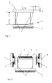
- FIG. 1 shows a plan view of a structure comprising a movable contact piece 1 with an elastic suspension 2.
- the viewing direction is perpendicular to the substrate plane, which should be a two-dimensional structure.
- the schematically drawn base 3 should, as indicated by the hatched background, be firmly connected to the substrate, whereas the elastic suspension forming carrier 2 and the movable contact piece 1 are free from the substrate.
- the parts 1, 2 and 3 should consist of Si and be worked out integrally from a Si substrate.
- the movable contact piece 1 and the carriers 2 have been freed from the substrate by dissolving an SiO 2 layer buried underneath.
- the solid lines represent the force-free arrangement, while the dashed lines the movable contact piece 1 and the elastic Show suspension 2 in the deflected state.
- This deflection is effected by a force symbolized by N, which acts from top to bottom in FIG. 1, So lies in the substrate plane, but to the difference between the dashed and the solid drawing recognizable Movement direction is substantially vertical.
- the direction of movement is By the way, not really constant direction. Rather, from this figure vividly that the direction of movement with increasing deflection of the right-angled orientation to the normal force away. However, it is essential that the moving distance is a much larger component f perpendicular to The force N contains as the force-parallel component ⁇ .
- the component ⁇ is but as important as it is necessary to the movement depicted at all with the force N to produce.
- the movement behavior of the movable contact piece 1 results from the Shape and arrangement of the pair of carriers 2 and these are in Movement direction spaced from each other and otherwise identical and to the force N substantially symmetrically aligned to Avoid torque as much as possible.
- the carriers 2 have a length I in Direction of the force N and are in contrast very narrow, as indicated by h.
- the depth perpendicular to the plane is denoted by b and corresponds here the depth of the movable contact piece 1. It is for the invention Principle not of concern.
- the area increases of the drive capacitor also linear with the depth, so that the depth b only from the technical limits of the etching process and the desired Contact surface depends.
- a too large width of the capacitor 4,5 increases not only the inertia of the movable contact part 1, but also goes directly into the overall size of the micro-relay.
- has a meaningful Compromise can be found.
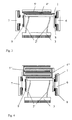
- FIG. 2 shows the basic structure schematically illustrated in FIG. 1 in a concrete application form.
- an electrically conductive surface layer 4 is mounted, which is opposite to a second electrically conductive surface layer 5 on a substrate-fixed part.
- A is the area of the drive capacitor 4, 5 and also proportional to b.
- d is the distance between the two drive capacitor surfaces 4 and 5. It can be seen immediately that very small by correspondingly small distances can generate large electrostatic forces, because the distance d in the second Potency occurs. Furthermore, wide capacitors in the sense of the horizontal in the Drawing plane, so large distances between the carriers 2, low. at a distance d of 1 .mu.m result at a supply voltage of 36 V and a typical area A of 450 ⁇ m x 1500 ⁇ m forces in the range of 4 mN.
- FIG. 2 shows that the movable contact piece 1 is switched back and forth between two counter-contact pieces 6 and 7.
- the movable contact piece 1 has, at its ends extending beyond the supports 2, in each case an angled attachment region 8 or 9, which carries in each case two metal contacts, which are connected via a metallic conductor track.
- These contacts can come in contact with each associated two contacts on the mating contact pieces 6 and 7, which in turn are electrically isolated from each other. They are thus bridged by the contacts on the angled regions 8 and 9 of the movable contact piece 1.
- the hatched areas in Figure 2 indicate that the two Drive capacitor surfaces 4 and 5 and in each case from the contacts to the Counter contact pieces 6 and 7 outgoing conductor tracks ion-implanted Si regions are formed.
- the black filled contacts are metallized, such as by lateral Schrägbedampfung or Plasma deposition and corresponding masking.
- the total contact surfaces by adjusting the Depth b can be determined.
- the metal contacts can also in the vertical direction in Figure 2 be made wider when the contact surface plays an essential role.
- the arrangement of the drive capacitor 4 '5' should be in simple micro-relay Incidentally, done so that when closed a maximum Contact force results, so the minimum distance between the Drive capacitor surfaces 4, 5 and 4 ', 5' is present. In the first and in the second embodiment, this is for the right switch and for the left Given a switch.
- Figure 4 shows a third embodiment, which is a variant of the second Embodiment of Figure 3 represents.
- the drive capacitor in this case of comb-like nested surfaces consisting of 4 "and 5". Again, these are Si structures with corresponding dopants (or metallizations), like the Show hatching.
- the drive capacitor By a manufacturing technology little problematic Complication of the mask layout can thus be effective Area of the drive capacitor can be multiplied, in this case tripled. Otherwise, this embodiment corresponds to the above described.
Landscapes
- Micromachines (AREA)
- Investigation Of Foundation Soil And Reinforcement Of Foundation Soil By Compacting Or Drainage (AREA)
- Relay Circuits (AREA)
Priority Applications (3)
| Application Number | Priority Date | Filing Date | Title |
|---|---|---|---|
| EP01810322A EP1246215B1 (fr) | 2001-03-29 | 2001-03-29 | Microrelais à nouvelle construction |
| DE50115251T DE50115251D1 (de) | 2001-03-29 | 2001-03-29 | Mikrorelais mit neuem Aufbau |
| AT01810322T ATE451712T1 (de) | 2001-03-29 | 2001-03-29 | Mikrorelais mit neuem aufbau |
Applications Claiming Priority (1)
| Application Number | Priority Date | Filing Date | Title |
|---|---|---|---|
| EP01810322A EP1246215B1 (fr) | 2001-03-29 | 2001-03-29 | Microrelais à nouvelle construction |
Publications (2)
| Publication Number | Publication Date |
|---|---|
| EP1246215A1 true EP1246215A1 (fr) | 2002-10-02 |
| EP1246215B1 EP1246215B1 (fr) | 2009-12-09 |
Family
ID=8183834
Family Applications (1)
| Application Number | Title | Priority Date | Filing Date |
|---|---|---|---|
| EP01810322A Expired - Lifetime EP1246215B1 (fr) | 2001-03-29 | 2001-03-29 | Microrelais à nouvelle construction |
Country Status (3)
| Country | Link |
|---|---|
| EP (1) | EP1246215B1 (fr) |
| AT (1) | ATE451712T1 (fr) |
| DE (1) | DE50115251D1 (fr) |
Cited By (3)
| Publication number | Priority date | Publication date | Assignee | Title |
|---|---|---|---|---|
| EP1463081A2 (fr) | 2003-03-25 | 2004-09-29 | Rockwell Automation Technologies, Inc. | Circuit d'isolement micro-éléctromécanique |
| WO2005015595A1 (fr) * | 2003-08-07 | 2005-02-17 | Fujitsu Limited | Microelement de commutation et procede de fabrication de cet element |
| WO2007059634A1 (fr) * | 2005-11-28 | 2007-05-31 | Abb Research Ltd | Actionneur electrostatique |
Citations (3)
| Publication number | Priority date | Publication date | Assignee | Title |
|---|---|---|---|---|
| WO1993003385A1 (fr) * | 1991-08-07 | 1993-02-18 | Robert Bosch Gmbh | Detecteur d'acceleration et procede de fabrication |
| US5375033A (en) * | 1992-04-14 | 1994-12-20 | Cornell Research Foundation, Inc. | Multi-dimensional precision micro-actuator |
| EP1020984A2 (fr) * | 1999-01-11 | 2000-07-19 | Samsung Electronics Co., Ltd. | Une structure de peine tridimensionnelle |
-
2001
- 2001-03-29 DE DE50115251T patent/DE50115251D1/de not_active Expired - Lifetime
- 2001-03-29 EP EP01810322A patent/EP1246215B1/fr not_active Expired - Lifetime
- 2001-03-29 AT AT01810322T patent/ATE451712T1/de not_active IP Right Cessation
Patent Citations (3)
| Publication number | Priority date | Publication date | Assignee | Title |
|---|---|---|---|---|
| WO1993003385A1 (fr) * | 1991-08-07 | 1993-02-18 | Robert Bosch Gmbh | Detecteur d'acceleration et procede de fabrication |
| US5375033A (en) * | 1992-04-14 | 1994-12-20 | Cornell Research Foundation, Inc. | Multi-dimensional precision micro-actuator |
| EP1020984A2 (fr) * | 1999-01-11 | 2000-07-19 | Samsung Electronics Co., Ltd. | Une structure de peine tridimensionnelle |
Cited By (4)
| Publication number | Priority date | Publication date | Assignee | Title |
|---|---|---|---|---|
| EP1463081A2 (fr) | 2003-03-25 | 2004-09-29 | Rockwell Automation Technologies, Inc. | Circuit d'isolement micro-éléctromécanique |
| EP1463081A3 (fr) * | 2003-03-25 | 2006-04-19 | Rockwell Automation Technologies, Inc. | Circuit d'isolement micro-éléctromécanique |
| WO2005015595A1 (fr) * | 2003-08-07 | 2005-02-17 | Fujitsu Limited | Microelement de commutation et procede de fabrication de cet element |
| WO2007059634A1 (fr) * | 2005-11-28 | 2007-05-31 | Abb Research Ltd | Actionneur electrostatique |
Also Published As
| Publication number | Publication date |
|---|---|
| EP1246215B1 (fr) | 2009-12-09 |
| DE50115251D1 (de) | 2010-01-21 |
| ATE451712T1 (de) | 2009-12-15 |
Similar Documents
| Publication | Publication Date | Title |
|---|---|---|
| DE60225484T2 (de) | Membranakivierter mikroelektromechanischer schalter | |
| EP0679878B1 (fr) | Microsystème avec circuit intégré et composante micromécanique et procédé de fabrication | |
| DE19954022B4 (de) | Halbleitersensor für eine physikalische Grösse und Verfahren zu dessen Herstellung | |
| WO1994019819A1 (fr) | Relais micromecanique a actionnement hybride | |
| DE112011102203B4 (de) | Elektromechanische Schaltereinheit und Verfahren zum Betätigen derselben | |
| DE10302618B4 (de) | Elektrostatische Betätigungsvorrichtung | |
| DE10031569A1 (de) | Integrierter Mikroschalter und Verfahren zu seiner Herstellung | |
| DE602005001745T2 (de) | Monolithische MEMS-Vorrichtung mit im Gleichgewicht befindlicher Kragplatte | |
| DE19823690C1 (de) | Mikromechanisches elektrostatisches Relais | |
| DE60308609T2 (de) | MEMS Schalter und Herstellungsverfahren | |
| DE60203021T2 (de) | Mikroeinstellbarer kondensator (mems) mit weitem variationsbereich und niedriger betätigungsspannung | |
| DE112011101117B4 (de) | Integrierter elektromechanischer Aktuator und Verfahren zur Herstellung desselben | |
| WO2000057445A1 (fr) | Microrelais fonctionnant par deplacement d'un element de contact parallelement a un substrat | |
| WO1999043013A1 (fr) | Relais micromecanique electrostatique | |
| EP1468436B1 (fr) | Systeme micro-electromecanique et procede de fabrication | |
| WO2021123147A1 (fr) | Élément piézoélectrique mobile et son procédé de production | |
| EP1246215B1 (fr) | Microrelais à nouvelle construction | |
| DE19800189C2 (de) | Mikromechanischer Schalter | |
| DE19920066B4 (de) | Sensor aus einem mehrschichtigen Substrat mit einem aus einer Halbleiterschicht herausstrukturierten Federelement | |
| EP4057317A1 (fr) | Élément commutateur mems encapsulé, dispositif et procédé de fabrication | |
| EP1191559A2 (fr) | Microcommutateur et son procédé de fabrication | |
| DE102004010150B9 (de) | Hochfrequenz-MEMS-Schalter mit gebogenem Schaltelement und Verfahren zu seiner Herstellung | |
| EP4002407A1 (fr) | Élément de commutation microélectromécanique, dispositif et procédé de fabrication | |
| EP1156504A2 (fr) | Relais micromécanique à commutation améliorée | |
| DE102008007345A1 (de) | Mikromechanisches Bauelement und Verfahren zur Herstellung desselben |
Legal Events
| Date | Code | Title | Description |
|---|---|---|---|
| PUAI | Public reference made under article 153(3) epc to a published international application that has entered the european phase |
Free format text: ORIGINAL CODE: 0009012 |
|
| AK | Designated contracting states |
Kind code of ref document: A1 Designated state(s): AT BE CH CY DE DK ES FI FR GB GR IE IT LI LU MC NL PT SE TR |
|
| AX | Request for extension of the european patent |
Free format text: AL;LT;LV;MK;RO;SI |
|
| 17P | Request for examination filed |
Effective date: 20030331 |
|
| AKX | Designation fees paid |
Designated state(s): AT BE CH CY DE DK ES FI FR GB GR IE IT LI LU MC NL PT SE TR |
|
| GRAP | Despatch of communication of intention to grant a patent |
Free format text: ORIGINAL CODE: EPIDOSNIGR1 |
|
| GRAS | Grant fee paid |
Free format text: ORIGINAL CODE: EPIDOSNIGR3 |
|
| GRAA | (expected) grant |
Free format text: ORIGINAL CODE: 0009210 |
|
| AK | Designated contracting states |
Kind code of ref document: B1 Designated state(s): AT BE CH CY DE DK ES FI FR GB GR IE IT LI LU MC NL PT SE TR |
|
| REG | Reference to a national code |
Ref country code: GB Ref legal event code: FG4D Free format text: NOT ENGLISH |
|
| REG | Reference to a national code |
Ref country code: CH Ref legal event code: EP |
|
| REG | Reference to a national code |
Ref country code: IE Ref legal event code: FG4D |
|
| REF | Corresponds to: |
Ref document number: 50115251 Country of ref document: DE Date of ref document: 20100121 Kind code of ref document: P |
|
| REG | Reference to a national code |
Ref country code: NL Ref legal event code: VDEP Effective date: 20091209 |
|
| PG25 | Lapsed in a contracting state [announced via postgrant information from national office to epo] |
Ref country code: FI Free format text: LAPSE BECAUSE OF FAILURE TO SUBMIT A TRANSLATION OF THE DESCRIPTION OR TO PAY THE FEE WITHIN THE PRESCRIBED TIME-LIMIT Effective date: 20091209 Ref country code: SE Free format text: LAPSE BECAUSE OF FAILURE TO SUBMIT A TRANSLATION OF THE DESCRIPTION OR TO PAY THE FEE WITHIN THE PRESCRIBED TIME-LIMIT Effective date: 20091209 |
|
| REG | Reference to a national code |
Ref country code: IE Ref legal event code: FD4D |
|
| PG25 | Lapsed in a contracting state [announced via postgrant information from national office to epo] |
Ref country code: NL Free format text: LAPSE BECAUSE OF FAILURE TO SUBMIT A TRANSLATION OF THE DESCRIPTION OR TO PAY THE FEE WITHIN THE PRESCRIBED TIME-LIMIT Effective date: 20091209 Ref country code: IE Free format text: LAPSE BECAUSE OF FAILURE TO SUBMIT A TRANSLATION OF THE DESCRIPTION OR TO PAY THE FEE WITHIN THE PRESCRIBED TIME-LIMIT Effective date: 20091209 Ref country code: ES Free format text: LAPSE BECAUSE OF FAILURE TO SUBMIT A TRANSLATION OF THE DESCRIPTION OR TO PAY THE FEE WITHIN THE PRESCRIBED TIME-LIMIT Effective date: 20100320 Ref country code: PT Free format text: LAPSE BECAUSE OF FAILURE TO SUBMIT A TRANSLATION OF THE DESCRIPTION OR TO PAY THE FEE WITHIN THE PRESCRIBED TIME-LIMIT Effective date: 20100409 |
|
| PGFP | Annual fee paid to national office [announced via postgrant information from national office to epo] |
Ref country code: DE Payment date: 20100419 Year of fee payment: 10 |
|
| BERE | Be: lapsed |
Owner name: ABB RESEARCH LTD. Effective date: 20100331 |
|
| PLBE | No opposition filed within time limit |
Free format text: ORIGINAL CODE: 0009261 |
|
| STAA | Information on the status of an ep patent application or granted ep patent |
Free format text: STATUS: NO OPPOSITION FILED WITHIN TIME LIMIT |
|
| PG25 | Lapsed in a contracting state [announced via postgrant information from national office to epo] |
Ref country code: MC Free format text: LAPSE BECAUSE OF NON-PAYMENT OF DUE FEES Effective date: 20100331 Ref country code: GR Free format text: LAPSE BECAUSE OF FAILURE TO SUBMIT A TRANSLATION OF THE DESCRIPTION OR TO PAY THE FEE WITHIN THE PRESCRIBED TIME-LIMIT Effective date: 20100310 Ref country code: CY Free format text: LAPSE BECAUSE OF FAILURE TO SUBMIT A TRANSLATION OF THE DESCRIPTION OR TO PAY THE FEE WITHIN THE PRESCRIBED TIME-LIMIT Effective date: 20091209 |
|
| REG | Reference to a national code |
Ref country code: CH Ref legal event code: PL |
|
| 26N | No opposition filed |
Effective date: 20100910 |
|
| GBPC | Gb: european patent ceased through non-payment of renewal fee |
Effective date: 20100329 |
|
| REG | Reference to a national code |
Ref country code: FR Ref legal event code: ST Effective date: 20101130 |
|
| PG25 | Lapsed in a contracting state [announced via postgrant information from national office to epo] |
Ref country code: DK Free format text: LAPSE BECAUSE OF FAILURE TO SUBMIT A TRANSLATION OF THE DESCRIPTION OR TO PAY THE FEE WITHIN THE PRESCRIBED TIME-LIMIT Effective date: 20091209 Ref country code: FR Free format text: LAPSE BECAUSE OF NON-PAYMENT OF DUE FEES Effective date: 20100331 |
|
| PG25 | Lapsed in a contracting state [announced via postgrant information from national office to epo] |
Ref country code: BE Free format text: LAPSE BECAUSE OF NON-PAYMENT OF DUE FEES Effective date: 20100331 Ref country code: CH Free format text: LAPSE BECAUSE OF NON-PAYMENT OF DUE FEES Effective date: 20100331 Ref country code: LI Free format text: LAPSE BECAUSE OF NON-PAYMENT OF DUE FEES Effective date: 20100331 |
|
| PG25 | Lapsed in a contracting state [announced via postgrant information from national office to epo] |
Ref country code: IT Free format text: LAPSE BECAUSE OF FAILURE TO SUBMIT A TRANSLATION OF THE DESCRIPTION OR TO PAY THE FEE WITHIN THE PRESCRIBED TIME-LIMIT Effective date: 20091209 Ref country code: GB Free format text: LAPSE BECAUSE OF NON-PAYMENT OF DUE FEES Effective date: 20100329 |
|
| PG25 | Lapsed in a contracting state [announced via postgrant information from national office to epo] |
Ref country code: AT Free format text: LAPSE BECAUSE OF NON-PAYMENT OF DUE FEES Effective date: 20100329 |
|
| PG25 | Lapsed in a contracting state [announced via postgrant information from national office to epo] |
Ref country code: DE Free format text: LAPSE BECAUSE OF NON-PAYMENT OF DUE FEES Effective date: 20111001 |
|
| REG | Reference to a national code |
Ref country code: DE Ref legal event code: R119 Ref document number: 50115251 Country of ref document: DE Effective date: 20111001 |
|
| PG25 | Lapsed in a contracting state [announced via postgrant information from national office to epo] |
Ref country code: LU Free format text: LAPSE BECAUSE OF NON-PAYMENT OF DUE FEES Effective date: 20100329 |
|
| PG25 | Lapsed in a contracting state [announced via postgrant information from national office to epo] |
Ref country code: TR Free format text: LAPSE BECAUSE OF FAILURE TO SUBMIT A TRANSLATION OF THE DESCRIPTION OR TO PAY THE FEE WITHIN THE PRESCRIBED TIME-LIMIT Effective date: 20091209 |