EP1246215A1 - Microrelay with new construction - Google Patents
Microrelay with new construction Download PDFInfo
- Publication number
- EP1246215A1 EP1246215A1 EP01810322A EP01810322A EP1246215A1 EP 1246215 A1 EP1246215 A1 EP 1246215A1 EP 01810322 A EP01810322 A EP 01810322A EP 01810322 A EP01810322 A EP 01810322A EP 1246215 A1 EP1246215 A1 EP 1246215A1
- Authority
- EP
- European Patent Office
- Prior art keywords
- contact piece
- micro
- movable contact
- movement
- drive capacitor
- Prior art date
- Legal status (The legal status is an assumption and is not a legal conclusion. Google has not performed a legal analysis and makes no representation as to the accuracy of the status listed.)
- Granted
Links
Images
Classifications
-
- H—ELECTRICITY
- H01—ELECTRIC ELEMENTS
- H01H—ELECTRIC SWITCHES; RELAYS; SELECTORS; EMERGENCY PROTECTIVE DEVICES
- H01H59/00—Electrostatic relays; Electro-adhesion relays
- H01H59/0009—Electrostatic relays; Electro-adhesion relays making use of micromechanics
-
- H—ELECTRICITY
- H01—ELECTRIC ELEMENTS
- H01H—ELECTRIC SWITCHES; RELAYS; SELECTORS; EMERGENCY PROTECTIVE DEVICES
- H01H1/00—Contacts
- H01H1/0036—Switches making use of microelectromechanical systems [MEMS]
- H01H2001/0078—Switches making use of microelectromechanical systems [MEMS] with parallel movement of the movable contact relative to the substrate
Abstract
Description
Diese Erfindung bezieht sich auf ein Mikrorelais mit einem neuen mechanischen Aufbau. Mit dem Begriff Mikrorelais bezeichnet man gewöhnlich mikroskopische elektrische Schalter, bei denen ein bewegbares Kontaktstück relativ zu einem Gegenkontaktstück elektrostatisch, elektromagnetisch, piezoelektrisch oder in anderer Weise bewegt wird, um einen elektrischen Kontakt zu öffnen und zu schließen. Mikrorelais sind also gewissermaßen sehr kleine Relais, wie sich schon aus dem Namen ergibt, und werden häufig, jedoch nicht notwendigerweise, unter Zuhilfenahme von technologischen Verfahren hergestellt, die der Halbleitertechnologie und/oder der Mikrostrukturtechnik entlehnt sind.This invention relates to a micro-relay with a new mechanical Construction. The term micro-relay is usually called microscopic electrical switches in which a movable contact piece relative to a Counter contact piece electrostatically, electromagnetically, piezoelectrically or in moved in any other way to open an electrical contact and to shut down. Micro relays are so to speak very small relays, like themselves even from the name results, and become common, but not necessarily, with the help of technological processes made of semiconductor technology and / or microstructure technology are borrowed.
Mikrorelais mit elektrostatischen Antrieben sind an sich bekannt. Der elektrostatische Antrieb wird durch einen Antriebskondensator bewirkt, der zwei beabstandete leitfähige Flächen aufweist, von denen eine mit dem bewegbaren Kontaktstück fest verbunden ist. Dadurch können die elektrostatischen Kräfte zwischen den Flächen zum mechanischen Antrieb des bewegbaren Kontaktstücks genutzt werden. Das bewegbare Kontaktstück ist dazu üblicherweise elastisch aufgehängt, so daß der elektrostatische Antrieb gegen eine Rückstellkraft der elastischen Aufhängung wirkt. Micro-relays with electrostatic drives are known per se. The electrostatic drive is effected by a drive capacitor, the two spaced conductive surfaces, one of which with the movable Contact piece is firmly connected. This allows the electrostatic forces between the surfaces for the mechanical drive of the movable Contact piece can be used. The movable contact piece is to Usually suspended elastically, so that the electrostatic drive against a restoring force of the elastic suspension acts.
Bei einigen bekannten Mikrorelais besteht das bewegbare Kontaktstück aus einer aus einer Substratoberfläche schräg herausstehenden Lamelle, die gleichzeitig eine der Antriebskondensatorflächen enthält, wobei die andere Antriebskondensatorfläche und das Gegenkontaktstück in der Substratebene angeordnet sind. Die elektrostatische Anziehungskraft zwischen den Antriebskondensatorflächen kann die Lamelle auf die Substratoberfläche herunterziehen, woraufhin ein Kontakt an dem lamellenartigen bewegbaren Kontaktstück das Gegenkontaktstück in der Substratoberfläche berührt.In some known micro-relay consists of the movable contact piece an obliquely protruding from a substrate surface lamella, the at the same time contains one of the drive capacitor surfaces, wherein the other Drive capacitor surface and the mating contact piece in the substrate plane are arranged. The electrostatic attraction between the Drive capacitor surfaces, the lamella on the substrate surface pull down, whereupon a contact on the lamellar movable Contact piece touches the mating contact piece in the substrate surface.
Der vorliegenden Erfindung liegt das technische Problem zugrunde, eine neuartige mechanische Bauform für ein Mikrorelais zur Verfügung zu stellen.The present invention is based on the technical problem, a novel mechanical design for a micro-relay to provide.
Dementsprechend ist erfindungsgemäß vorgesehen ein Mikrorelais mit einem bewegbaren Kontaktstück, einem Antriebskondensator zum elektrostatischen Antrieb des bewegbaren Kontaktstücks, welcher Antriebskondensator im wesentlichen parallel beabstandete, leitfähige Flächen aufweist, von denen eine mit dem bewegbaren Kontaktstück fest verbunden ist, einer elastischen Aufhängung des bewegbaren Kontaktstücks und einem Gegenkontaktstück, wobei das Mikrorelais so ausgelegt ist, daß durch Ändern des Ladezustands des Antriebskondensators das bewegbare Kontaktstück in einer Bewegungsrichtung in eine und aus einer Anlage an das Gegenkontaktstück bewegt werden kann, um einen elektrischen Kontakt zwischen dem bewegbaren Kontaktstück und dem Gegenkontaktstück zu öffnen und zu schließen, bei dem die Bewegungsrichtung zu der Richtung des Abstandes zwischen den Antriebskondensatorflächen fast senkrecht ist und die elastische Aufhängung bezüglich einer Bewegung des bewegbaren Kontaktstücks in der Bewegungsrichtung eine Federkonstante aufweist, die wesentlich kleiner ist als eine Federkonstante der elastischen Aufhängung bezüglich einer Bewegung in der Richtung des Abstandes der Antriebskondensatorflächen.Accordingly, the invention provides a micro-relay with a movable contact piece, a drive capacitor for electrostatic Drive of the movable contact piece, which drive capacitor in having substantially parallel spaced, conductive surfaces, one of which is firmly connected to the movable contact piece, an elastic Suspension of the movable contact piece and a mating contact piece, wherein the micro-relay is designed so that by changing the state of charge of the Drive capacitor, the movable contact piece in a direction of movement can be moved in and out of a system to the mating contact piece, to an electrical contact between the movable contact piece and the mating contact to open and close, in which the Direction of movement to the direction of the distance between the Drive capacitor surfaces is almost vertical and the elastic suspension with respect to a movement of the movable contact piece in the Direction of movement has a spring constant, which is much smaller than a spring constant of the elastic suspension with respect to a movement in the direction of the distance of the drive capacitor surfaces.
Die Grundidee der Erfindung liegt also darin, von dem konventionellen Konzept abzurücken, bei dem die Bewegungsrichtung des bewegbaren Kontaktstücks im wesentlichen gleich gerichtet bzw. parallel zu der elektrostatischen Kraft ist. Erfindungsgemäß wird vielmehr ein Aufbau gewählt, bei dem das bewegbare Kontaktstück elastisch so aufgehängt ist, daß es eine im Bezug zu der Richtung der elektrostatischen Kraft, also zu der dem direkten Abstand zwischen den Antriebskondensatorflächen entsprechenden Richtung, querelastisch ist. Bei dieser Querelastizität muß jedoch eine geringe Komponente in Kraftrichtung vorhanden sein, so daß die Antriebskondensatorflächen aneinander angenähert oder voneinander entfernt werden. Wesentlich ist jedoch, daß der bei weitem überwiegende Teil der Bewegung des bewegbaren Kontaktstücks senkrecht zu der elektrostatischen Kraft, also dem Kondensatorzwischenabstand, liegt. Quantitativ kann das bedeuten, daß die Querkomponente bei den Bewegungen insgesamt vorzugsweise zumindest das 5-fache, besser das 7,5-fache, noch besser das 12-fache und im günstigsten Fall sogar mehr als das 20-fache der kraftparallelen Komponente beträgt. Dies wird erfindungsgemäß dadurch erreicht, daß die elastische Aufhängung in der gewünschten Bewegungsrichtung eine sehr viel kleinere Federkonstante aufweist als in der (konventionellen) Richtung des Abstandes zwischen den Antriebskondensatorflächen.The basic idea of the invention is therefore that of the conventional concept to move away, in which the direction of movement of the movable contact piece in is substantially equal or parallel to the electrostatic force. Rather, a structure is chosen according to the invention, in which the movable Contact piece is elastically suspended so that it is one with respect to the direction the electrostatic force, ie to the direct distance between the Drive capacitor surfaces corresponding direction, is transverse elastic. at However, this transverse elasticity must have a low component in the direction of force be present so that the drive capacitor surfaces approach each other or removed from each other. It is essential, however, that by far most of the movement of the movable contact piece perpendicular to the electrostatic force, so the capacitor gap is. Quantitatively, this may mean that the transverse component in the movements Overall, preferably at least 5 times, more preferably 7.5 times, still better 12 times and in the best case even more than 20 times the force-parallel component is. This is inventively characterized achieved that the elastic suspension in the desired direction of movement has a much smaller spring constant than in the (conventional) Direction of the distance between the drive capacitor surfaces.
Die Vorteile dieses Aufbaus können verschiedenartig sein: Zum einen kann es bei manchen Anwendungsfällen zu günstigeren geometrischen Lösungen führen, die Antriebskondensatorflächen im wesentlichen parallel zu der Bewegungsrichtung des bewegbaren Kontaktstücks anordnen zu können. Die Erfindung stellt also einen neuen Freiheitsgrad für den Entwurf von Mikrorelais zur Verfügung. The advantages of this structure can be varied: For one thing it can in some applications to more favorable geometric solutions lead, the drive capacitor surfaces substantially parallel to the Movement direction of the movable contact piece to order. The The invention thus provides a new degree of freedom for the design of micro-relays to disposal.
Ein wesentlicher, jedoch erfindungsgemäß nicht notwendigerweise im Vordergrund stehender Vorteil besteht darin, daß durch die relativ kleine Komponente der Bewegungen des bewegbaren Kontaktstücks in der Richtung des Abstands der Antriebskondensatorflächen mit dem erfindungsgemäßen Mikrorelais relativ große quantitative Verhältnisse zwischen der möglichen Bewegungsstrecke des bewegbaren Kontaktstücks einerseits und dem maximal auftretenden Zwischenabstand zwischen den Antriebskondensatorflächen andererseits erzielt werden können. Nach einem bevorzugten Gesichtspunkt der Erfindung sollen diese quantitativen Verhältnisse möglichst groß sein, vorzugsweise über 10, besser über 20 und am besten über 40. Dies hat nämlich zur Folge, daß einerseits mit relativ kleinen Versorgungsspannungen ausreichend große elektrostatische Kräfte zwischen den Antriebskondensatorflächen erzeugt werden können, andererseits die Isolationsabstände zwischen dem bewegbaren Kontaktstück und dem Gegenkontaktstück, die ja von dem bewegbaren Kontaktstück bei der Bewegung überwunden werden müssen, dennoch relativ groß ausfallen können. Die erfindungsgemäßen Mikrorelais können also eine hohe Spannungsfestigkeit mit einer kleinen Antriebsspannung kombinieren.An essential, but not necessarily according to the invention in Foremost advantage is that through the relatively small Component of the movements of the movable contact piece in the direction the distance of the drive capacitor surfaces with the inventive Microrelay relatively large quantitative ratios between the possible Moving distance of the movable contact piece on the one hand and the maximum occurring intermediate distance between the drive capacitor surfaces On the other hand can be achieved. According to a preferred aspect of Invention, these quantitative ratios should be as large as possible, preferably over 10, better over 20 and best over 40. This is because As a result, on the one hand with relatively small supply voltages sufficiently large electrostatic forces between the Drive capacitor surfaces can be generated, on the other hand, the Isolation distances between the movable contact piece and the Counter contact piece, yes of the movable contact piece in the movement must be overcome, but can be relatively large. The Microrelay according to the invention can thus with a high dielectric strength combine a small drive voltage.
Damit wird ein Hauptnachteil elektrostatischer Mikrorelais überwunden, die zwar konventionellerweise bereits relativ niedrige Versorgungsspannungen bzw.leistungen ermöglichen, jedoch im Hinblick auf die Spannungsfestigkeit dahingehend begrenzt sind, daß der Antriebskondensator auch bei dem größten auftretenden Abstand zwischen den Antriebskondensatorflächen noch eine ausreichend große anziehende Kraft aufbringen können muß.This overcomes a major disadvantage of electrostatic micro-relays, which are Conventionally, already relatively low supply voltages or services allow, however, in terms of dielectric strength are limited to the effect that the drive capacitor even at the largest occurring distance between the drive capacitor surfaces yet another must be able to muster sufficiently large attractive force.
Im übrigen können mit den konventionellen elektrostatischen Mikrorelais im Vergleich zu den elektromagnetischen Antriebslösungen nur sehr kleine Andruckkräfte zwischen den Kontakten, also zwischen dem bewegbaren Kontaktstück und dem Gegenkontaktstück, aufgebracht werden. Aus diesen relativ geringen Kontaktkräften können Schwierigkeiten in der Herstellung der Kontakte und unerwünscht hohe Kontaktwiderstände entstehen. Auch hier bietet die Erfindung eine Abhilfsmöglichkeit.Incidentally, with the conventional electrostatic microrelay in the Compared to the electromagnetic drive solutions only very small Pressure forces between the contacts, ie between the movable Contact piece and the mating contact piece to be applied. From these relatively low contact forces can cause difficulties in the production of Contacts and undesirable high contact resistance arise. Also here offers the invention a remedy.
Eine günstige Ausführungsform für eine elastische Aufhängung mit den beschriebenen Eigenschaften besteht aus zumindest einem schmalen langen Träger, dessen Längsrichtung der Richtung des Abstandes der Antriebskondensatorflächen entspricht und der in der Bewegungsrichtung des bewegbaren Kontaktstücks sehr viel schmaler ist. In der dritten verbleibenden Richtung kann der Träger relativ ausgedehnt sein oder auch relativ flach sein, vorzugsweise angepaßt an die entsprechenden Abmessungen des Antriebskondensators und der übrigen Bauteile in dieser Richtung. Dieser Träger bildet eine blattfederähnliche Struktur und kann durch die elektrostatische Kraft des Antriebskondensators zwar nicht verlängert und verkürzt, jedoch seitlich verformt werden.A favorable embodiment of an elastic suspension with the described properties consists of at least a narrow long Beam whose longitudinal direction of the distance of the Drive capacitor areas corresponds and in the direction of movement of the movable contact piece is much narrower. In the third remaining Direction, the carrier may be relatively extended or relatively flat, preferably adapted to the corresponding dimensions of Drive capacitor and the other components in this direction. This carrier forms a leaf-spring-like structure and can be affected by the electrostatic force Although the drive capacitor is not extended and shortened, but laterally be deformed.
Vorzugsweise sind zumindest zwei dieser Träger vorgesehen, die vorzugsweise im wesentlichen identisch miteinander, jedoch in der Bewegungsrichtung voneinander beabstandet sind. Durch ihre gemeinsame feste Kopplung mit dem bewegbaren Kontaktstück ergibt sich dann eine Bewegung des bewegbaren Kontaktstücks, die verkippungsfrei bleibt, also im wesentlichen nur aus translatorischen Komponenten besteht. Hierzu wird auf die Ausführungsbeispiele verwiesen. Die Kraft-Weg-Zusammenhänge, also die Federkonstanten, können bei solchen Trägem anhand bekannter Näherungsformeln leicht berechnet werden.Preferably, at least two of these carriers are provided, which are preferably essentially identical to each other, but in the direction of movement spaced apart from each other. Through their common solid coupling with the movable contact piece then results in a movement of the movable Contact piece, which remains tilt-free, so essentially only off translational components. For this purpose, the embodiments directed. The force-distance relationships, so the spring constants can in such carriers easily calculated using known approximation formulas become.
Die Bewegung des bewegbaren Kontaktstücks kann nicht nur dazu genutzt werden, einen an dem bewegbaren Kontaktstück angebrachten Kontakt mit einem zugeordneten Kontakt an einem Gegenkontaktstück in Verbindung zu bringen und ihn davon zu trennen, vielmehr kann die selbe Bewegung gleichzeitig einen weiteren Kontakt des bewegbaren Kontaktstücks mit einem anderen Kontakt an einem weiteren Gegenkontaktstück in komplementärer Weise verbinden und trennen. Dabei wird also das bewegbare Kontaktstück zwischen den Gegenkontaktstücken hin- und herbewegt. Man erhält gewissermaßen einen Doppelschalter, der zudem in einer Mittenposition einen Zustand bietet, in dem sämtliche Kontakte getrennt sind. Er kann jedoch auch so ausgelegt sein oder betrieben werden, daß er zwischen zwei Zuständen geschaltet wird, in denen jeweils eines der beiden Kontaktpaare offen und das jeweils andere geschlossen ist. Die verschiedenen vorteilhaften Anwendungsmöglichkeiten solcher Doppelschalter sind dem Fachmann ohne weiteres bekannt.The movement of the movable contact piece can not only be used for this purpose be, attached to the movable contact piece contact with an associated contact on a mating contact in connection to bring and separate him from it, rather, the same movement can at the same time a further contact of the movable contact piece with a other contact on another mating contact in complementary Connect and disconnect. In this case, therefore, the movable contact piece moved back and forth between the mating contact pieces. You get in a sense, a double switch, which also in a middle position one State offers, in which all contacts are separated. But he can do that too be designed or operated to be between two states is switched, in each case one of the two contact pairs open and the each other is closed. The different advantageous ones Applications of such double switch are the expert without further known.
Der oder die beschriebenen Träger müssen übrigens im kräftefreien Zustand nicht notwendigerweise grade langgestreckt sein, so daß sie durch den elektrostatischen Antrieb verkrümmt werden. Sie können auch bei der Herstellung des Mikrorelais bereits mit einer vorgegebenen leichten Krümmung versehen sein, die dann durch die elektrostatische Antriebskraft verringert, aufgehoben oder auch im Richtungssinn umgekehrt werden kann.Incidentally, the carrier or carriers described must be in a force-free state not necessarily elongated, so that they through the electrostatic drive are curved. You can also at the Production of the micro-relay already with a predetermined slight curvature be provided, which then reduces by the electrostatic driving force, canceled or can be reversed in the direction sense.
Weiterhin ist es denkbar, den Antriebskondensator komplizierter auszuführen als lediglich mit zwei benachbarten Antriebskondensatorflächen. Es können auch verschachtelte Strukturen Verwendung finden, bei denen eine größere Zahl Antriebskondensatorflächen in verschachtelter Weise einander zugeordnet sind, etwa wie zwei miteinander in Eingriff gebrachte Kämme. Zur Veranschaulichung wird auf das entsprechende Ausführungsbeispiel verwiesen.Furthermore, it is conceivable to make the drive capacitor more complicated than only with two adjacent drive capacitor surfaces. It can too nested structures find use where a larger number Drive capacitor surfaces are associated in an interleaved manner, like two combs engaged with each other. As an illustration Reference is made to the corresponding embodiment.
Die Bewegungsrichtung des erfindungsgemäßen Mikrorelais liegt vorzugsweise parallel zu einem Substrat, auf dem das Mikrorelais angebracht ist oder auf dem es vorzugsweise integriert hergestellt worden ist. Auch hierin besteht ein Unterschied zum Stand der Technik, bei dem die Bewegungsrichtungen mehr oder weniger senkrecht zur Substratebene liegen. Die substratparallele Bewegungsrichtung hat jedoch den Vorteil, zweidimensionale Strukturen des Mikrorelais zu begünstigen, die herstellungstechnisch sehr vorteilhaft sind. So sind die typischen mikrotechnologischen und halbleitertechnologischen Verfahren wie Lithographie-, Ätz- oder Beschichtungsverfahren in der Regel zunächst zweidimensional und bei dreidimensionalen Strukturen nur mit etwas erhöhtem Aufwand zu realisieren. Dementsprechend sind die einzelnen Funktionsteile des Mikrorelais, nämlich das bewegbare Kontaktstück, die elastische Aufhängung sowie der Antriebskondensator, jeweils in ihrer funktionalen Struktur vorzugsweise rein zweidimensional, und zwar in einer substratparallelen Ebene.The direction of movement of the micro-relay according to the invention is preferably parallel to a substrate on which the micro-relay is mounted or on the it has preferably been produced integrated. This also exists Difference to the prior art, in which the directions of movement more or less perpendicular to the substrate plane. The substrate parallel Movement direction, however, has the advantage of two-dimensional structures of the To encourage micro-relays, which are very advantageous in terms of manufacturing technology. So are the typical microtechnological and semiconductor technology Processes such as lithography, etching or coating process usually initially two-dimensional and in three-dimensional structures only with something to realize increased effort. Accordingly, the individual Functional parts of the micro-relay, namely the movable contact piece, the elastic suspension and the drive capacitor, each in their functional structure preferably purely two-dimensional, in one substrate-parallel plane.
Ferner ist ein durch die substratparallele Bewegung möglicher flacher Aufbau häufig bautechnisch günstig und erleichtert insbesondere nachfolgende Lithographieschritte, etwa solche, die für auf dem selben Substrat herzustellende mikroelektronische Schaltungen benötigt werden. Auch bei einem Schutz des Mikrorelais durch eine Verkapselung oder Abdeckung ist ein flacher Aufbau vorteilhaft.Furthermore, a flat construction possible by the substrate-parallel movement is possible often structurally favorable and facilitates in particular subsequent Lithography steps, such as those to be prepared for on the same substrate microelectronic circuits are needed. Even with a protection of Micro-relay through an encapsulation or cover is a flat construction advantageous.
Um die bewegbaren Teile des Mikrorelais bei einer integrierten Ausführungsform vom Substrat zu lösen, bietet es sich an, vergrabene Schichten an den geeigneten Stellen vorzusehen und zu entfernen, um diese Teile vom Substrat zu befreien und damit elastisch verformbar bzw. bewegbar zu machen. Hier bieten sich insbesondere SiO2-Schichten bei Siliziumsubstraten an. Insbesondere bieten sich hierzu die bekannten SOI-Strukturen (Silicon on Insulator) an, und zwar vor allem die sogenannten SIMOX-Wafer.In order to detach the movable parts of the micro-relay from the substrate in an integrated embodiment, it is advisable to provide and remove buried layers at the suitable locations in order to free these parts from the substrate and thus make them elastically deformable or movable. In particular, SiO 2 layers are suitable for silicon substrates. In particular, the well-known SOI structures (Silicon on Insulator) are suitable for this purpose, especially the so-called SIMOX wafers.
Der Werkstoff Silizium ist grundsätzlich ein bevorzugter Werkstoff für das erfindungsgemäße Mikrorelais. The material silicon is basically a preferred material for the Micro-relay according to the invention.
Eine andere Werkstofflösung sind verschiedene Gläser. Silizium hat allerdings den Vorteil, durch geeignete Sortierung sowohl isolierend als auch elektrisch leitfähig ausgeführt werden zu können. Durch lonenimplantation oder Diffusion von Dotierungsstoffen können somit Leiterbahnen mit angepaßter Struktur leicht hergestellt werden. Die zugrundeliegende Technologie ist aus der Halbleiterbauelementherstellung bekannt.Another material solution are different glasses. Silicon, however, has the advantage of suitable sorting both insulating and electric be carried out conductive. By ion implantation or diffusion Of dopants can thus easily conductive tracks with adapted structure getting produced. The underlying technology is from the Semiconductor device manufacturing known.
Trotzdem werden beispielsweise für die Kontakte selbst Metallisierungen notwendig sein. Bei einem gläsernen Mikrorelais müssen grundsätzlich Metallisierungen angebracht werden, um die elektrischen Leitungen und Kontakte herzustellen.Nevertheless, for example, for the contacts themselves metallizations to be necessary. In a glass micro-relay must basically Metallizations are attached to the electrical wires and Make contacts.
Besondere Bedeutung für die Herstellung des erfindungsgemäßen Mikrorelais, insbesondere bei einer zweidimensionalen Realisierung mit substratparalleler Ausrichtung, haben die lonenätzverfahren, und zwar insbesondere die sogenannten RIE-Verfahren. Da für das Mikrorelais relativ große Ätztiefen interessant sein können, kommen bevorzugt die sogenannten DRIE-Verfahren in Betracht (deep reactive ion etching). Durch geeignete Prozeßführung lassen sich in erheblichen Tiefen nahezu senkrechte Ätzflanken erzielen, beispielsweise in der Größenordnung von 0,5 mm. Dies kann zur Erzielung ausreichend großer Kontaktflächen wichtig sein, weil sich bei den bevorzugten Ausführungsformen der Erfindung senkrecht auf dem Substrat stehende Kontaktflächen ergeben können. Hierzu wird wiederum auf die Ausführungsbeispiele verwiesen.Particular importance for the production of the micro-relay according to the invention, in particular in a two-dimensional realization with substrate-parallel Alignment, have the ion etching, and in particular the so-called RIE procedure. As for the micro-relay relatively large etching depths may be interesting, come preferably the so-called DRIE method Deep reactive ion etching. By suitable process control can be Achieve near vertical etching edges in considerable depths, for example in of the order of 0.5 mm. This can be sufficiently large to achieve Contact areas are important because in the preferred embodiments of the invention provide perpendicular contact surfaces on the substrate can. For this purpose, reference is again made to the exemplary embodiments.
Als Beispiel wird ferner verwiesen auf den Artikel "Vertical Mirrors Fabricated by Deep Reactive Ion Etching for Fiber Optic Switching Applications". Von C. Marxer at all, Journal of Microelectromechanical Systems, Band 6, Nr. 3, September 1997, Seiten 277 - 285. Dort sind zwar mikrooptische Schalter für faseroptische Anwendungen beschrieben, jedoch lassen sich die Prozeßschritte auch ohne weiteres auf die Erfindung anwenden. Die dort realisierten Wandhöhen von 75 Mikrometer lassen sich leicht übertreffen, wenn dies von Interesse ist.As an example, reference is also made to the article "Vertical Mirrors Fabricated by Deep Reactive Ion Etching for Fiber Optic Switching Applications "by C. Marxer at all, Journal of Microelectromechanical Systems, Vol. 6, No. 3, September 1997, pages 277 - 285. There are indeed micro-optical switches for Fiber optic applications described, however, the process steps can be also readily apply to the invention. The realized there Wall heights of 75 microns can be easily surpassed, if this from Interest is.
Im folgenden werden Ausführungsbeispiele der Erfindung erläutert, wobei die dabei offenbarten Merkmale auch in anderen als den dargestellten Kombinationen erfindungswesentlich sein können.In the following, embodiments of the invention are explained, wherein the thereby revealed features in other than the illustrated Combinations may be essential to the invention.
Im einzelnen zeigt:
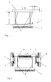
Figur 1 zeigt eine Draufsicht auf eine Struktur aus einem bewegbaren
Kontaktstück 1 mit elastischer Aufhängung 2. Die Blickrichtung steht senkrecht
auf der Substratebene, wobei es sich um eine zweidimensionale Struktur
handeln soll. Die schematisch eingezeichnete Basis 3 soll, wie durch den
schraffierten Untergrund angedeutet, fest mit dem Substrat verbunden sein,
wohingegen die elastische Aufhängung bildende Träger 2 und das bewegbare
Kontaktstück 1 von dem Substrat frei sind. Bei dem konkreten Beispiel sollen die
Teile 1, 2 und 3 aus Si bestehen und integriert aus einem Si-Substrat
herausgearbeitet sein. Das bewegbare Kontaktstück 1 und die Träger 2 sind von
dem Substrat durch Lösen einer darunter vergrabenen SiO2-Schicht befreit
worden.FIG. 1 shows a plan view of a structure comprising a
Die durchgezogenen Linien stellen dabei die kräftefreie Anordnung dar, während
die gestrichelten Linien das bewegbare Kontaktstück 1 und die elastische
Aufhängung 2 in ausgelenktem Zustand zeigen. Diese Auslenkung wird bewirkt
durch eine mit N symbolisierte Kraft, die in Figur 1 von oben nach unten wirkt,
also in der Substratebene liegt, jedoch zu der durch den Unterschied zwischen
der gestrichelten und der durchgezogenen Zeichnung erkennbaren
Bewegungsrichtung im wesentlichen senkrecht steht. Die Bewegungsrichtung ist
dabei übrigens keine wirklich konstante Richtung. Vielmehr ist aus dieser Figur
anschaulich, daß sich die Bewegungsrichtung mit zunehmender Auslenkung von
der rechtwinkligen Orientierung zur Normalkraft entfernt. Wesentlich ist jedoch,
daß die Bewegungsstrecke eine sehr viel größere Komponente f senkrecht zu
der Kraft N enthält als die kraftparallele Komponente λ. Die Komponente λ ist
jedoch insoweit wichtig, als sie notwendig ist, um die dargestellte Bewegung
überhaupt mit der Kraft N erzeugen zu können.The solid lines represent the force-free arrangement, while
the dashed lines the
Das Bewegungsverhalten des bewegbaren Kontaktstücks 1 ergibt sich aus der
Form und Anordnung des Paares der Träger 2 und diese sind in
Bewegungsrichtung voneinander beabstandet und dabei im übrigen identisch
sowie zu der Kraft N im wesentlichen symmetrisch ausgerichtet, um
Drehmomente möglichst zu vermeiden. Die Träger 2 haben eine Länge I in
Richtung der Kraft N und sind demgegenüber sehr schmal, wie mit h bezeichnet.
Die Tiefe senkrecht zur Zeichenebene ist mit b bezeichnet und entspricht hier
der Tiefe des bewegbaren Kontaktstücks 1. Sie ist für das erfindungsgemäße
Prinzip nicht weiter von Belang. Wie sich weiter unten ergibt, erhöht sie zwar die
Federkonstante linear, jedoch wächst bei den Ausführungsbeispielen die Fläche
des Antriebskondensators ebenfalls linear mit der Tiefe, so daß die Tiefe b nur
von den technischen Grenzen des Ätzverfahrens und der gewünschten
Kontaktfläche abhängt. Eine zu große Breite des Kondensators 4,5 erhöht aber
nicht nur die Massenträgheit des bewegbaren Kontaktteils 1, sondern geht auch
direkt in die Gesamtbaugröße des Mikrorelais ein. Hier muß also ein sinnvoller
Kompromiß gefunden werden.The movement behavior of the
Die Auslenkung f in der gewünschten kraftnormalen Dimension errechnet sich
näherungsweise aus
Dabei ist E der Elastizitätsmodul des verwendeten Materials. Man erkennt, daß
die Tiefe b linear in die Federkonstante eingeht, diese jedoch in der dritten
Potenz von dem Verhältnis aus Länge I und Schmalheit h der Träger 2 abhängt.
Die notwendige, jedoch möglichst kleine Bewegungskomponente λ beträgt
näherungsweise
Man sieht, daß die Bewegung in zunehmendem Maße von der senkrechten Ausrichtung zur Kraft N abweicht, weil die Komponente λ proportional zum Quadrat der Komponente f ist. Man erkennt außerdem, daß lange Träger günstig sind für eine großes Verhältnis aus der kraftnormalen Komponente f zu der kraftparallelen Komponente λ.It can be seen that the movement is increasingly dependent on the vertical Orientation to force N differs because the component λ proportional to Square of the component f is. It also recognizes that long vehicles are cheap are for a large ratio of the normal component f to the force-parallel component λ.
Quantitative Beispielswerte könnten eine Länge von I = 1800 µm, eine Schmalheit h von 16 µm und eine Tiefe b von 450 µm sein. Ein beispielhafter Wert für die Kraft N von etwa 4 mN führt dann zu f = 40 µm und λ = 0,53 µm. Die Bewegung des bewegbaren Kontaktschubs 1 ist also so gut wie senkrecht zu N. Quantitative example values could have a length of I = 1800 μm, a Be narrowness h of 16 microns and a depth b of 450 microns. An exemplary Value for the force N of about 4 mN then leads to f = 40 μm and λ = 0.53 μm. The Movement of the movable contact thrust 1 is thus as good as perpendicular to N.
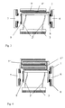
Figur 2 zeigt die schematisch in Figur 1 erläuterte Grundstruktur in einer
konkreten Anwendungsform. An dem bewegbaren Kontaktstück 1 ist, in diesem
Fall an der den Trägern 2 zugewandten Seite, eine elektrisch leitfähige
Oberflächenschicht 4 angebracht, der eine zweite elektrisch leitfähige
Oberflächenschicht 5 an einem substratfesten Teil gegenüber liegt. Zwischen
diesen beiden Antriebskondensatorflächen 4 und 5 kann eine Spannung Ud
angelegt werden, die die elektrostatische Antriebskraft N gemäß folgendem
Näherungszusammenhang hervorruft:
Dabei ist A die Fläche des Antriebskondensators 4, 5 und ebenfalls proportional
zu b. d ist der Abstand zwischen den beiden Antriebskondensatorflächen 4 und
5. Man erkennt unmittelbar, daß sich durch entsprechend kleine Abstände sehr
große elektrostatische Kräfte erzeugen lassen, weil der Abstand d in der zweiten
Potenz auftritt. Ferner sind breite Kondensatoren im Sinn der Horizontalen in der
Zeichenebene, also große Abstände zwischen den Trägern 2, günstig. Bei
einem Abstand d von 1 µm ergeben sich bei einer Versorgungsspannung von 36
V und einer typischen Fläche A von 450 µm x 1500 µm Kräfte im Bereich von 4
mN.Here, A is the area of the
Die Bewegung des bewegbaren Kontaktstücks 1 entspricht der Darstellung in
Figur 1. Figur 2 zeigt, daß das bewegbare Kontaktstück 1 dabei zwischen zwei
Gegenkontaktstücken 6 und 7 hin- und hergeschaltet wird. Hierzu weist es an
seinen über die Träger 2 hinausreichenden Enden jeweils einen abgewinkelten
Ansatzbereich 8 bzw. 9 auf, der jeweils zwei metallene Kontakte, die über eine
metallische Leiterbahn verbunden sind, trägt. Diese Kontakte können in Kontakt
mit jeweils zugeordneten zwei Kontakten auf den Gegenkontaktstücken 6 und 7
kommen, die jedoch ihrerseits elektrisch voneinander isoliert sind. Sie werden
also durch die Kontakte auf den abgewinkelten Bereichen 8 bzw. 9 des
bewegbaren Kontaktstücks 1 überbrückt. Die Kontaktkraft P ergibt sich dabei
aus
Die schraffierten Bereiche in Figur 2 deuten dabei an, daß die beiden
Antriebskondensatorflächen 4 und 5 sowie jeweils von den Kontakten an den
Gegenkontaktstücken 6 und 7 ausgehende Leiterbahnen durch
ionenimplantierte Si-Bereiche gebildet sind. Die schwarz ausgefüllten Kontakte
sind metallisiert, etwa durch seitliche Schrägbedampfung oder
Plasmaabscheidung und entsprechende Maskierung.The hatched areas in Figure 2 indicate that the two
Drive capacitor surfaces 4 and 5 and in each case from the contacts to the
Man erkennt ferner, daß das Mikrorelais aus Figur 2 bei ungeladenem
Antriebskondensator 4, 5 die Kontakte an dem linken Gegenkontaktstück 7
überbrückt und durch Spannungsbeaufschlagung des Kondensators 4, 5 so
umgeschaltet werden kann, daß statt dessen die Kontakte an dem rechten
Gegenkontaktstück 6 überbrückt werden. Die Antriebskondensatorflächen 4, 5
sind dabei so zueinander ausgerichtet, daß sie einander etwa in der Mitte dieses
Weges direkt gegenüber liegen, so daß jeweils an den beiden Wegenden ein
gewisser Versatz vorliegt, der jedoch wegen der tatsächlich geringen
quantitativen Bedeutung unwesentlich ist.It can also be seen that the micro-relay of Figure 2 in
Es wurde bereits erwähnt, daß die Gesamtkontaktflächen durch Anpassung der Tiefe b bestimmt werden können. Außerdem können die Metallkontakte auch in der in Figur 2 vertikalen Richtung breiter ausgeführt sein, wenn die Kontaktfläche eine wesentliche Rolle spielt. It has already been mentioned that the total contact surfaces by adjusting the Depth b can be determined. In addition, the metal contacts can also in the vertical direction in Figure 2 be made wider when the contact surface plays an essential role.
Wenn man sich einen der beiden abgewinkelten Bereiche 8 und 9 und das
zugehörige Gegenkontaktstück 6 bzw. 7 in Figur 2 wegdenkt, so erkennt man
unmittelbar, daß sich mit diesem Aufbau auch einfache Schalter realisieren
lassen, die wahlweise im spannungslosen Zustand offen oder geschlossen sind
(normally open / normally closed).If you look at one of the two
Bei dem zweiten Ausführungsbeispiel aus Figur 3 liegt gegenüber den Varianten aus Figur 1 und 2 dahingehend eine Abweichung vor, daß die Träger 2' nur mehr im dargestellten spannungsfreien Zustand leicht S-förmig gekrümmt sind, nämlich etwa so, wie im verformten Zustand aus Figur 1. Dies kann durch entsprechende Strukturierung der Maske bei dem DRIE-Prozeß, mit dem diese Strukturen aus dem Siliziumwafer herausgearbeitet werden, leicht realisiert werden. Außerdem ist der Antriebskondensator bei diesem Beispiel auf der im Vergleich zu Figur 2 anderen Seite des bewegbaren Kontaktstücks 1 angeordnet, und daher mit 4', 5' bezeichnet. Schließlich ist das Mikrorelais in diesem Fall so ausgelegt, daß der "rechte Schalter" 6, 8 im spannungsfreien Zustand geschlossen ist, während der "linke Schalter" 7, 9 im spannungsfreien Zustand offen ist.In the second embodiment of Figure 3 is opposite to the variants from Figure 1 and 2 to the effect that before the carrier 2 'only are slightly curved slightly S-shaped in the illustrated stress-free state, namely, approximately as in the deformed state of Figure 1. This can by corresponding structuring of the mask in the DRIE process, with which this Structures are machined out of the silicon wafer, easily realized become. In addition, the drive capacitor in this example is on in the Comparison to Figure 2 other side of the movable contact piece. 1 arranged, and therefore designated 4 ', 5'. Finally, the micro-relay is in This case designed so that the "right switch" 6, 8 in the tension-free Condition is closed while the "left switch" 7, 9 in the tension-free Condition is open.
Durch die elektrostatische Anziehung zwischen den Antriebskondensatorflächen
4' und 5' kann das bewegbare Kontaktstück 1 in Figur 3 nach links bewegt
werden, wobei sich die Träger 2' weitgehend strecken bzw. auch mit
umgekehrtem Richtungssinn verformen können.Due to the electrostatic attraction between the drive capacitor surfaces
4 'and 5', the
Die Anordnung des Antriebskondensators 4' 5' sollte bei einfachen Mikrorelais übrigens so erfolgen, daß sich im geschlossenen Zustand eine maximale Kontaktkraft ergibt, also der minimale Abstand zwischen den Antriebskondensatorflächen 4, 5 bzw. 4', 5' vorliegt. Bei dem ersten und bei dem zweiten Ausführungsbeispiel ist dies für den rechten Schalter bzw. für den linken Schalter gegeben. The arrangement of the drive capacitor 4 '5' should be in simple micro-relay Incidentally, done so that when closed a maximum Contact force results, so the minimum distance between the Drive capacitor surfaces 4, 5 and 4 ', 5' is present. In the first and in the second embodiment, this is for the right switch and for the left Given a switch.
Figur 4 zeigt ein drittes Ausführungsbeispiel, das eine Variante zu dem zweiten Ausführungsbeispiel aus Figur 3 darstellt. Der Unterschied besteht darin, daß der Antriebskondensator in diesem Fall aus kammartig verschachtelten Flächen besteht, die mit 4" und 5" bezeichnet sind. Es handelt sich wiederum um Si-Strukturen mit entsprechenden Dotierungen (oder Metallisierungen), wie die Schraffuren zeigen. Durch eine herstellungstechnisch wenig problematische Komplizierung des Maskenlayouts kann so die zuvor mit A bezeichnete effektive Fläche des Antriebskondensators vervielfacht werden, in diesem Fall verdreifacht. Im übrigen entspricht dieses Ausführungsbeispiel dem zuvor beschriebenen.Figure 4 shows a third embodiment, which is a variant of the second Embodiment of Figure 3 represents. The difference is that the drive capacitor in this case of comb-like nested surfaces consisting of 4 "and 5". Again, these are Si structures with corresponding dopants (or metallizations), like the Show hatching. By a manufacturing technology little problematic Complication of the mask layout can thus be effective Area of the drive capacitor can be multiplied, in this case tripled. Otherwise, this embodiment corresponds to the above described.
Alle Ausführungsbeispiele sind infolge des zweidimensionalen Aufbaus technisch unproblematisch und zeigen andererseits einen ungewöhnlich guten Kompromiß zwischen Kontaktschließkraft, Versorgungsspannung und Spannungsfestigkeit im geöffneten Zustand.All embodiments are due to the two-dimensional structure technically unproblematic and on the other hand show an unusually good Compromise between contact closure force, supply voltage and Dielectric strength in the open state.
- 11
- bewegbares Kontaktstückmovable contact piece
- 22
- elastische Aufhängung, nämlich schmale lange Trägerelastic suspension, namely narrow long straps
- 33
- BasisBase
- 4, 4', 4"4, 4 ', 4 "
- leitfähige Kondensatorfläche am bewegbaren Kontaktstückconductive capacitor surface on the movable contact piece
- 5, 5', 5"5, 5 ', 5 "
- feste elektrisch leitfähige Antriebskondensatorflächesolid electrically conductive drive capacitor surface
- 6, 76, 7
- GegenkontaktstückeAgainst contacts
- 8, 98, 9
- abgewinkelte Ansatzbereiche des bewegbaren KontaktstücksAngled approach areas of the movable contact piece
- ff
- Bewegungsstrecke quer zur KraftMovement distance across the force
- II
-
Länge eines Trägers 2Length of a
carrier 2 - hH
-
Schmalheit eines Trägers 2Narrowness of a
carrier 2
Claims (14)
Priority Applications (3)
| Application Number | Priority Date | Filing Date | Title |
|---|---|---|---|
| DE50115251T DE50115251D1 (en) | 2001-03-29 | 2001-03-29 | Micro relay with new construction |
| EP01810322A EP1246215B1 (en) | 2001-03-29 | 2001-03-29 | Microrelay with new construction |
| AT01810322T ATE451712T1 (en) | 2001-03-29 | 2001-03-29 | MICRO RELAY WITH NEW CONSTRUCTION |
Applications Claiming Priority (1)
| Application Number | Priority Date | Filing Date | Title |
|---|---|---|---|
| EP01810322A EP1246215B1 (en) | 2001-03-29 | 2001-03-29 | Microrelay with new construction |
Publications (2)
| Publication Number | Publication Date |
|---|---|
| EP1246215A1 true EP1246215A1 (en) | 2002-10-02 |
| EP1246215B1 EP1246215B1 (en) | 2009-12-09 |
Family
ID=8183834
Family Applications (1)
| Application Number | Title | Priority Date | Filing Date |
|---|---|---|---|
| EP01810322A Expired - Lifetime EP1246215B1 (en) | 2001-03-29 | 2001-03-29 | Microrelay with new construction |
Country Status (3)
| Country | Link |
|---|---|
| EP (1) | EP1246215B1 (en) |
| AT (1) | ATE451712T1 (en) |
| DE (1) | DE50115251D1 (en) |
Cited By (3)
| Publication number | Priority date | Publication date | Assignee | Title |
|---|---|---|---|---|
| EP1463081A2 (en) | 2003-03-25 | 2004-09-29 | Rockwell Automation Technologies, Inc. | Microelectromechanical isolating circuit |
| WO2005015595A1 (en) * | 2003-08-07 | 2005-02-17 | Fujitsu Limited | Micro switching element and method of manufacturing the element |
| WO2007059634A1 (en) * | 2005-11-28 | 2007-05-31 | Abb Research Ltd | Electrostatic actuator |
Citations (3)
| Publication number | Priority date | Publication date | Assignee | Title |
|---|---|---|---|---|
| WO1993003385A1 (en) * | 1991-08-07 | 1993-02-18 | Robert Bosch Gmbh | Acceleration sensor and process for its production |
| US5375033A (en) * | 1992-04-14 | 1994-12-20 | Cornell Research Foundation, Inc. | Multi-dimensional precision micro-actuator |
| EP1020984A2 (en) * | 1999-01-11 | 2000-07-19 | Samsung Electronics Co., Ltd. | A 3-dimensional comb structure |
-
2001
- 2001-03-29 DE DE50115251T patent/DE50115251D1/en not_active Expired - Lifetime
- 2001-03-29 EP EP01810322A patent/EP1246215B1/en not_active Expired - Lifetime
- 2001-03-29 AT AT01810322T patent/ATE451712T1/en not_active IP Right Cessation
Patent Citations (3)
| Publication number | Priority date | Publication date | Assignee | Title |
|---|---|---|---|---|
| WO1993003385A1 (en) * | 1991-08-07 | 1993-02-18 | Robert Bosch Gmbh | Acceleration sensor and process for its production |
| US5375033A (en) * | 1992-04-14 | 1994-12-20 | Cornell Research Foundation, Inc. | Multi-dimensional precision micro-actuator |
| EP1020984A2 (en) * | 1999-01-11 | 2000-07-19 | Samsung Electronics Co., Ltd. | A 3-dimensional comb structure |
Cited By (4)
| Publication number | Priority date | Publication date | Assignee | Title |
|---|---|---|---|---|
| EP1463081A2 (en) | 2003-03-25 | 2004-09-29 | Rockwell Automation Technologies, Inc. | Microelectromechanical isolating circuit |
| EP1463081A3 (en) * | 2003-03-25 | 2006-04-19 | Rockwell Automation Technologies, Inc. | Microelectromechanical isolating circuit |
| WO2005015595A1 (en) * | 2003-08-07 | 2005-02-17 | Fujitsu Limited | Micro switching element and method of manufacturing the element |
| WO2007059634A1 (en) * | 2005-11-28 | 2007-05-31 | Abb Research Ltd | Electrostatic actuator |
Also Published As
| Publication number | Publication date |
|---|---|
| DE50115251D1 (en) | 2010-01-21 |
| EP1246215B1 (en) | 2009-12-09 |
| ATE451712T1 (en) | 2009-12-15 |
Similar Documents
| Publication | Publication Date | Title |
|---|---|---|
| DE60225484T2 (en) | MEMBRANE-ACTIVATED MICROELECTROMECHANICAL SWITCH | |
| EP0679878B1 (en) | Microsystem with integrated circuit and micromechanical component and fabrication procedure | |
| DE19954022B4 (en) | Semiconductor physical quantity sensor and method of making the same | |
| WO1994019819A1 (en) | Micromechanical relay with hybrid actuator | |
| DE112011102203B4 (en) | Electromechanical switch unit and method for actuating the same | |
| DE10302618B4 (en) | Electrostatic actuator | |
| DE10031569A1 (en) | Highly miniaturized relay in integrated circuit form, providing reliable operation and high isolation at high frequencies, includes see-saw mounted plate alternately closing contacts on substrate when rocked | |
| DE602005001745T2 (en) | Monolithic MEMS device with balanced cantilever plate | |
| DE19823690C1 (en) | Micromechanical electrostatic relay | |
| DE60308609T2 (en) | MEMS switch and manufacturing process | |
| DE60203021T2 (en) | MICRO-ADJUSTABLE CAPACITOR (MEMS) WITH LARGE VARIATION RANGE AND LOW OPERATING VOLTAGE | |
| DE112011101117B4 (en) | Integrated electromechanical actuator and method of making the same | |
| WO2000057445A1 (en) | Microrelay working parallel to the substrate | |
| WO1999043013A1 (en) | Micro-mechanical electrostatic relay | |
| WO2021123147A1 (en) | Movable piezo element and method for producing a movable piezo element | |
| EP1246215B1 (en) | Microrelay with new construction | |
| EP1468436A1 (en) | Micro-electromechanical system and method for production thereof | |
| DE19800189C2 (en) | Micromechanical switch | |
| DE19920066B4 (en) | Sensor comprising a multilayer substrate with a spring element structured out of a semiconductor layer | |
| EP4057317A1 (en) | Encapsulated mems switching element, device and manufacturing method | |
| DE19937811C2 (en) | Relays, in particular micro relays for forming a circuit | |
| EP1191559A2 (en) | Micro-switch and method of manufacturing the same | |
| DE102008007345B4 (en) | Micromechanical component and method for producing the same | |
| DE102004010150B9 (en) | High-frequency MEMS switch with bent switching element and method for its production | |
| EP4002407A1 (en) | Microelectromechanical switching element, device and manufacturing method |
Legal Events
| Date | Code | Title | Description |
|---|---|---|---|
| PUAI | Public reference made under article 153(3) epc to a published international application that has entered the european phase |
Free format text: ORIGINAL CODE: 0009012 |
|
| AK | Designated contracting states |
Kind code of ref document: A1 Designated state(s): AT BE CH CY DE DK ES FI FR GB GR IE IT LI LU MC NL PT SE TR |
|
| AX | Request for extension of the european patent |
Free format text: AL;LT;LV;MK;RO;SI |
|
| 17P | Request for examination filed |
Effective date: 20030331 |
|
| AKX | Designation fees paid |
Designated state(s): AT BE CH CY DE DK ES FI FR GB GR IE IT LI LU MC NL PT SE TR |
|
| GRAP | Despatch of communication of intention to grant a patent |
Free format text: ORIGINAL CODE: EPIDOSNIGR1 |
|
| GRAS | Grant fee paid |
Free format text: ORIGINAL CODE: EPIDOSNIGR3 |
|
| GRAA | (expected) grant |
Free format text: ORIGINAL CODE: 0009210 |
|
| AK | Designated contracting states |
Kind code of ref document: B1 Designated state(s): AT BE CH CY DE DK ES FI FR GB GR IE IT LI LU MC NL PT SE TR |
|
| REG | Reference to a national code |
Ref country code: GB Ref legal event code: FG4D Free format text: NOT ENGLISH |
|
| REG | Reference to a national code |
Ref country code: CH Ref legal event code: EP |
|
| REG | Reference to a national code |
Ref country code: IE Ref legal event code: FG4D |
|
| REF | Corresponds to: |
Ref document number: 50115251 Country of ref document: DE Date of ref document: 20100121 Kind code of ref document: P |
|
| REG | Reference to a national code |
Ref country code: NL Ref legal event code: VDEP Effective date: 20091209 |
|
| PG25 | Lapsed in a contracting state [announced via postgrant information from national office to epo] |
Ref country code: FI Free format text: LAPSE BECAUSE OF FAILURE TO SUBMIT A TRANSLATION OF THE DESCRIPTION OR TO PAY THE FEE WITHIN THE PRESCRIBED TIME-LIMIT Effective date: 20091209 Ref country code: SE Free format text: LAPSE BECAUSE OF FAILURE TO SUBMIT A TRANSLATION OF THE DESCRIPTION OR TO PAY THE FEE WITHIN THE PRESCRIBED TIME-LIMIT Effective date: 20091209 |
|
| REG | Reference to a national code |
Ref country code: IE Ref legal event code: FD4D |
|
| PG25 | Lapsed in a contracting state [announced via postgrant information from national office to epo] |
Ref country code: NL Free format text: LAPSE BECAUSE OF FAILURE TO SUBMIT A TRANSLATION OF THE DESCRIPTION OR TO PAY THE FEE WITHIN THE PRESCRIBED TIME-LIMIT Effective date: 20091209 Ref country code: IE Free format text: LAPSE BECAUSE OF FAILURE TO SUBMIT A TRANSLATION OF THE DESCRIPTION OR TO PAY THE FEE WITHIN THE PRESCRIBED TIME-LIMIT Effective date: 20091209 Ref country code: ES Free format text: LAPSE BECAUSE OF FAILURE TO SUBMIT A TRANSLATION OF THE DESCRIPTION OR TO PAY THE FEE WITHIN THE PRESCRIBED TIME-LIMIT Effective date: 20100320 Ref country code: PT Free format text: LAPSE BECAUSE OF FAILURE TO SUBMIT A TRANSLATION OF THE DESCRIPTION OR TO PAY THE FEE WITHIN THE PRESCRIBED TIME-LIMIT Effective date: 20100409 |
|
| PGFP | Annual fee paid to national office [announced via postgrant information from national office to epo] |
Ref country code: DE Payment date: 20100419 Year of fee payment: 10 |
|
| BERE | Be: lapsed |
Owner name: ABB RESEARCH LTD. Effective date: 20100331 |
|
| PLBE | No opposition filed within time limit |
Free format text: ORIGINAL CODE: 0009261 |
|
| STAA | Information on the status of an ep patent application or granted ep patent |
Free format text: STATUS: NO OPPOSITION FILED WITHIN TIME LIMIT |
|
| PG25 | Lapsed in a contracting state [announced via postgrant information from national office to epo] |
Ref country code: MC Free format text: LAPSE BECAUSE OF NON-PAYMENT OF DUE FEES Effective date: 20100331 Ref country code: GR Free format text: LAPSE BECAUSE OF FAILURE TO SUBMIT A TRANSLATION OF THE DESCRIPTION OR TO PAY THE FEE WITHIN THE PRESCRIBED TIME-LIMIT Effective date: 20100310 Ref country code: CY Free format text: LAPSE BECAUSE OF FAILURE TO SUBMIT A TRANSLATION OF THE DESCRIPTION OR TO PAY THE FEE WITHIN THE PRESCRIBED TIME-LIMIT Effective date: 20091209 |
|
| REG | Reference to a national code |
Ref country code: CH Ref legal event code: PL |
|
| 26N | No opposition filed |
Effective date: 20100910 |
|
| GBPC | Gb: european patent ceased through non-payment of renewal fee |
Effective date: 20100329 |
|
| REG | Reference to a national code |
Ref country code: FR Ref legal event code: ST Effective date: 20101130 |
|
| PG25 | Lapsed in a contracting state [announced via postgrant information from national office to epo] |
Ref country code: DK Free format text: LAPSE BECAUSE OF FAILURE TO SUBMIT A TRANSLATION OF THE DESCRIPTION OR TO PAY THE FEE WITHIN THE PRESCRIBED TIME-LIMIT Effective date: 20091209 Ref country code: FR Free format text: LAPSE BECAUSE OF NON-PAYMENT OF DUE FEES Effective date: 20100331 |
|
| PG25 | Lapsed in a contracting state [announced via postgrant information from national office to epo] |
Ref country code: BE Free format text: LAPSE BECAUSE OF NON-PAYMENT OF DUE FEES Effective date: 20100331 Ref country code: CH Free format text: LAPSE BECAUSE OF NON-PAYMENT OF DUE FEES Effective date: 20100331 Ref country code: LI Free format text: LAPSE BECAUSE OF NON-PAYMENT OF DUE FEES Effective date: 20100331 |
|
| PG25 | Lapsed in a contracting state [announced via postgrant information from national office to epo] |
Ref country code: IT Free format text: LAPSE BECAUSE OF FAILURE TO SUBMIT A TRANSLATION OF THE DESCRIPTION OR TO PAY THE FEE WITHIN THE PRESCRIBED TIME-LIMIT Effective date: 20091209 Ref country code: GB Free format text: LAPSE BECAUSE OF NON-PAYMENT OF DUE FEES Effective date: 20100329 |
|
| PG25 | Lapsed in a contracting state [announced via postgrant information from national office to epo] |
Ref country code: AT Free format text: LAPSE BECAUSE OF NON-PAYMENT OF DUE FEES Effective date: 20100329 |
|
| PG25 | Lapsed in a contracting state [announced via postgrant information from national office to epo] |
Ref country code: DE Free format text: LAPSE BECAUSE OF NON-PAYMENT OF DUE FEES Effective date: 20111001 |
|
| REG | Reference to a national code |
Ref country code: DE Ref legal event code: R119 Ref document number: 50115251 Country of ref document: DE Effective date: 20111001 |
|
| PG25 | Lapsed in a contracting state [announced via postgrant information from national office to epo] |
Ref country code: LU Free format text: LAPSE BECAUSE OF NON-PAYMENT OF DUE FEES Effective date: 20100329 |
|
| PG25 | Lapsed in a contracting state [announced via postgrant information from national office to epo] |
Ref country code: TR Free format text: LAPSE BECAUSE OF FAILURE TO SUBMIT A TRANSLATION OF THE DESCRIPTION OR TO PAY THE FEE WITHIN THE PRESCRIBED TIME-LIMIT Effective date: 20091209 |