EP1245922B1 - System for measuring phase differences in reflected light signals - Google Patents
System for measuring phase differences in reflected light signals Download PDFInfo
- Publication number
- EP1245922B1 EP1245922B1 EP02006807A EP02006807A EP1245922B1 EP 1245922 B1 EP1245922 B1 EP 1245922B1 EP 02006807 A EP02006807 A EP 02006807A EP 02006807 A EP02006807 A EP 02006807A EP 1245922 B1 EP1245922 B1 EP 1245922B1
- Authority
- EP
- European Patent Office
- Prior art keywords
- light signal
- reflected
- laser
- slope
- polarized light
- Prior art date
- Legal status (The legal status is an assumption and is not a legal conclusion. Google has not performed a legal analysis and makes no representation as to the accuracy of the status listed.)
- Expired - Lifetime
Links
Images


Classifications
-
- G—PHYSICS
- G01—MEASURING; TESTING
- G01B—MEASURING LENGTH, THICKNESS OR SIMILAR LINEAR DIMENSIONS; MEASURING ANGLES; MEASURING AREAS; MEASURING IRREGULARITIES OF SURFACES OR CONTOURS
- G01B11/00—Measuring arrangements characterised by the use of optical techniques
- G01B11/02—Measuring arrangements characterised by the use of optical techniques for measuring length, width or thickness
- G01B11/06—Measuring arrangements characterised by the use of optical techniques for measuring length, width or thickness for measuring thickness ; e.g. of sheet material
- G01B11/0616—Measuring arrangements characterised by the use of optical techniques for measuring length, width or thickness for measuring thickness ; e.g. of sheet material of coating
-
- H—ELECTRICITY
- H01—ELECTRIC ELEMENTS
- H01L—SEMICONDUCTOR DEVICES NOT COVERED BY CLASS H10
- H01L22/00—Testing or measuring during manufacture or treatment; Reliability measurements, i.e. testing of parts without further processing to modify the parts as such; Structural arrangements therefor
- H01L22/10—Measuring as part of the manufacturing process
- H01L22/12—Measuring as part of the manufacturing process for structural parameters, e.g. thickness, line width, refractive index, temperature, warp, bond strength, defects, optical inspection, electrical measurement of structural dimensions, metallurgic measurement of diffusions
-
- H—ELECTRICITY
- H01—ELECTRIC ELEMENTS
- H01L—SEMICONDUCTOR DEVICES NOT COVERED BY CLASS H10
- H01L2924/00—Indexing scheme for arrangements or methods for connecting or disconnecting semiconductor or solid-state bodies as covered by H01L24/00
- H01L2924/0001—Technical content checked by a classifier
- H01L2924/0002—Not covered by any one of groups H01L24/00, H01L24/00 and H01L2224/00
Definitions
- the present invention is directed toward measuring thin films and defects on silicon wafers, magnetic thin film disks and transparent and coated glass substrates and more particularly toward measuring thin film thickness, and wear, surface roughness, scratches, particles, stains, pits, mounds, surface topography, step heights, and inclusions using a laser directed toward a thin film disk at many angles including non-Brewster's angles of an absorbing layer of the thin film.
- Coated thin film disks are used in a variety of industries including the semiconductor and the magnetic hard disk industry.
- a computer hard disk (magnetic storage device) is a non-volatile memory device that can store large amounts of data.
- One problem that the manufacturers of hard disks experience is how to maximize the operating life of a hard disk. When a hard disk fails the data stored therein may be difficult, expensive, or impossible to retrieve. Failure of a hard disk may be caused by defects on the surface of the thin film disk. It is crucial to be able to detect and classify these defects in order to prevent disk drive failure and to control the manufacturing process.
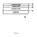
- FIG. 1 A schematic of a thin film disk used in magnetic storage devices is shown in Figure 1 . It includes a magnetic thin film (layer) 106 which is deposited upon a substrate 108 (typically a NiP plated Al-Mg alloy or glass).
- the magnetic thin film 106 can be protected by a thin film of carbon 104 (carbon layer), for example, whose thickness is typically 20 to 200 Angstroms ( ⁇ ).
- the carbon layer 104 is typically coated with a thin layer (10 to 30 Angstroms) of a fluorocarbon lubricant 102 (lubricant layer).
- the lubricant layer 102 serves to increase the durability of the underlying carbon layer 104 particularly when the magnetic read/write head contacts the disk, for example when the disk drive is turned off.
- the hard disk drive industry has been dramatically improving storage capacity by flying the thin film head closer to the surface of the thin film disk. As a result even very small defects can cause a hard drive to fail. These defects may be topographic such as scratches, pits, mounds, or particles or they may be non-topographic such as stains or inclusions. It is necessary to measure all these types of defects to control the disk manufacturing process and improve disk drive manufacturing yield.
- FIG. 2 A schematic of a semiconductor wafer is shown in Figure 2 .
- the structure of a semiconductor wafer can be very complex and Figure 2 shows only one example of a wafer that is undergoing the copper dual damascene process.
- a copper layer 201 a second plasma enhanced chemical vapor deposited (PECVD) oxide layer 202, a first PECVD oxide layer 203 and is a silicon substrate 204.
- the copper layer 201 is polished using a chemical mechanical polishing (CMP) process until only the via holes and copper lines remain.
- CMP chemical mechanical polishing
- the problem is that the CMP process can leave residual copper, nitride, or CMP slurry on the surface of the wafer.
- stains, particles, scratches, and micro-waviness may be present on the polished wafer. It is necessary to detect and measure such defects to control the process of making the wafer. Fewer defects will also mean greater wafer yields at the end of the process.
- a problem in the hard disk, semiconductor and photonics industries is to inspect these magnetic disks and wafers for defects such as particles, scratches, pits, mounds, stains, topographic irregularities and inclusions.
- Conventional techniques to solve these problems are discussed in U.S Patent No. 4,674,875, U.S. Patent No. 5,694,214 , U.S. Patent No. 5,748,305 , and U.S. Patent No. 6,157,444 .
- These patents describe techniques to measure defects using essentially sophisticated scatterometers and reflectometers. None of these systems enables the simultaneous measurement of topographic and non-topographic defects. This invention enables this measurement through the use of a combined reflectometer, scatterometer, ellipsometer, profilometer and Kerr effect microscope.
- US Patent No. 6,134,011 discloses an optical measurement system for evaluating the surface of a substrate or the thickness and optical characteristics of a thin film layer overlying the substrate. It includes an intensity stabilized light source configured to generate a stabilized light beam, a polarizing element for polarizing the light beam emanating from the light source, and a detection system for measuring the light reflected from the substrate. Furthermore, it includes a polarizing beam-splitter for splitting the light reflected from the substrate into S-polarized light and P-polarized light.
- US Patent No. 5,995,226 discloses an optical apparatus for measuring profiles for wafer including a pair of optical profile measuring systems which are provided at positions faced to both sides of a wafer vertically supported at its edge.
- US 4,906,844 discloses a method of monitoring the thickness of a growing layer during the fabrication of an optical thin film.
- the method comprises a step of directing a beam of circularly polarized monochromatic monitoring light having an S polarized component with a first phase and a P polarized component with a second phase into the layer.
- the reflected portion of the light is divided into two portions by a polarizing beam splitter.
- the beam splitter is rotated about the axis of reflected beams so that the beam is divided into a component polarized at + 45° with respect to the P polarization direction of the reflected beam and a component polarized at - 45° with respect to the P polarization.
- Two detectors indicate the amount of each component of the reflected light. When the amounts are equal, the phase shift is zero and the thickness of the layer is an integer multiple of one fourth the wavelength of the particular light selected by a monochrometer.
- What is needed is a system for examining thin film disks, silicon wafers and transparent wafers that: (1) measures topographic and non-topographic defects; (2) measures the optical profile on these substrates; (3) enables the measurements to be performed simultaneously; (4) measures the thickness of thin films; (4) enables measurement on patterned or unpatterned silicon or photonic wafers; (5) is performed in situ or in line .
- the present invention provides a system for measuring a phase shift according to claim 1.
- a system for measuring topographic and non-topographic defects and topography on thin film magnetic disks, silicon wafers and transparent substrates is provided.
- This invention enables the measurement of the height of a defect on a thin film disk or a silicon wafer having a first electromagnetic signal source for generating a first signal toward a first position on the thin film magnetic disk at a first angle, a second electromagnetic signal source for generating a second signal toward the first position on the thin film magnetic disk at a second angle, a spinning device for rotating the object to change the first position, a first position sensitive detector to receive a portion of said first signal that reflects off of the object, and to determine a radial portion of the first signal (S1r) and a circumferential portion of said first signal (S1c), a second position sensitive detector positioned at a right angle from the first position sensitive detector, to receive a reflected portion of the second signal that reflects off of the object, and to determine a radial portion of the second signal (S2r) and a circumferential
- the system also includes a processor for determining the height of the first position based upon a difference between S2c and S1c that does not include slope information.
- the system also enables the detection of topographic and non-topographic defects through the measurement of the phase shift of the optical wave.
- a feature of this invention is its ability to remove a semiconductor pattern from the data and enhance the ability to detect the presence of defects on the patterned silicon or photonics wafer.
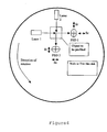
- Figure 3 is an illustration of an apparatus for measuring properties of the thin film according to an embodiment of the present invention.
- the apparatus uses a focused laser light signal whose angle of propagation ⁇ (as shown in Figure 3 ) can be between zero degrees from normal and ninety degrees from normal.
- One embodiment of the apparatus 300 includes a conventional laser diode 301, e.g., RLD65MZT1 or RLD-78MD available from Rolm Corporation, Kyoto, Japan, which has been collimated by Hoetron Corp., Sunnyvale, California, e.g., a conventional linear polarizer 302, e.g., made of Polarcor that is commercially available from Newport Corp., Irvine, California, a conventional zero order half wave plate 303 that is commercially available from CVI Laser, Livermore CA, a conventional focusing lens 304 that is commercially available from Newport Corporation, Irvine, California, conventional mirrors 305 and 308 available from Newport Corp. Irving, CA.
- a conventional laser diode 301 e.g., RLD65MZT1 or RLD-78MD available from Rolm Corporation, Kyoto, Japan, which has been collimated by Hoetron Corp., Sunnyvale, California
- a conventional linear polarizer 302 e.g., made of Polarcor that is commercially available from
- the apparatus 300 is an embodiment of the present invention and that alternate designs can be used without departing from the present invention. The operation of the apparatus 300 is now described in greater detail.
- a laser diode 301 emits an electromagnetic signal toward the thin film disk, silicon wafer, photonics wafer or glass substrate 306.
- the electromagnetic signal is a light signal having a wavelength of 780 or 655 nanometers (nm) although a wide variety of wavelengths can be used.
- the angle of propagation of the light signal can be any angle ⁇ between zero and ninety degrees.
- Laser diodes are well known to have an internal photodiode to monitor the laser output power.
- An embodiment of a feedback control circuit to control the optical intensity is to use such a photodiode, which is internal to the laser diode.
- This photodiode which is internal to the laser diode feeds back a control signal to negative feedback circuitry and by doing so keeps the intensity of the laser at a constant value.
- Another means of keeping an approximate constant output power of the laser is to control the current of the laser diode, that is, run the diode laser in a constant current mode.
- the laser diode will exhibit a very slow decrease in output power over a period of months. As long as the scan time is less than 5 or 10 minutes then the optical power output of the laser will remain constant during the scan.
- the advantage of this technique is its simplicity.
- Long-term drifts of the laser output power may be calibrated out of the system by first measuring a standard reflector and using this to normalize the measured signals. The value of the signal is first measured over the standard (known) reflector and then the disk or wafer is measured. If there has been any drift of the standard reflector measurement then all the data is corrected for this amount of drift. As a result long-term drifts may be compensated even when operating in a constant current mode.
- the emitted light passes through the linear polarizer 302.
- the linear polarizer 302 improves the linear polarization of the laser light signal.
- the linearly polarized light passes through a mechanically rotatable zero order half-wave plate 303.
- the half wave plate 303 is attached to a miniature motor 315 which allows the polarization to be dynamically rotated between P polarized (parallel to the plane of incidence), S polarized (perpendicular to the plane of incidence) and 45° polarized (between P and S) light.
- the polarized light passes through a focussing lens 304 and is directed onto a thin film magnetic disk, silicon wafer or transparent substrate 306 by a turning mirror 305.
- the reflected signal is directed to the detection optics by another turning mirror 308 and recollimated by another lens 309.
- the scattered component of the signal is detected by an avalanche photodiode 314.
- the recollimated beam passes through a zero order quarter wave plate 310 that is used to adjust the polarization of the beam so that equal amounts of energy are directed into the quadrant photodetectors 313 and 311.
- the beam is split by a polarization beam splitter 312 that is rotated by 45° to the plane of incidence.
- the polarizing beam splitter may be a Wollaston prism or a Glan Thompson or a Rochon prism beam splitter.
- the split beams are directed onto two quadrant detectors 311 and 313.
- the quadrant detectors are used to compute the phase shift between the split beams, the reflectivity, the optical profiles in the radial and circumferential directions, and the Kerr rotation (if the film on the substrate 306 is magnetic).
- the outputs from the quadrant detectors are digitized by a conventional analog to digital converter and directed to the memory of a conventional personal computer.
- the signals are then analyzed by the personal computer to detect defects, measure topography, and measure stains.
- the entire optical apparatus 300 is placed upon a stage that moves the apparatus in the radial direction while a motor 307 rotates the sample 306. In this manner the entire surface of the sample 306 may be scanned for defects.
- the spindle or motor which rotates the disk at a high rate of speed contains an encoder which produces 1024 pulses as it rotates through 360 degrees, for example.
- This encoder is used to determine the circumferential positions around the disk.
- the present invention preferably utilizes a very high-resolution determination of the position around the circumference of the disk. This is accomplished by using a phase locked loop to multiply the encoder signal by a selectable factor.
- the phase locked loop which multiplies the 1024 encoder pulses, has the ability to track any velocity jitter in the encoder. This feature allows averaging of repeated revolutions to be done with no loss of lateral resolution. That is, subsequent revolutions lie in phase with one another and when averaged, the resulting image is not smeared by any jitter effect. Averaging is done to improve signal-to-noise ratio.
- Figure 4 shows the top view design of an exemplifying optical profilometer useful for understanding the invention, which is capable of only measuring the height and directly measuring the height, that is, it can measure the height without measuring the slope. It can also measure the slope of the surface independent of height. This differs from previous optical profilometers that measure both slope and height simultaneously. With such systems the height is obtained from the slope data by integrating the slope information. However, if the slope information is contaminated with height information then the integration will not give the correct surface profile. The problem is to obtain data that contains only height information and not a combination of both slope and height.
- the design illustrated and described with reference to Figures 4-7 accomplishes this by using two lasers and two position sensitive detectors (PSD) oriented at right angles to one another.
- PSD position sensitive detector
- PSD position sensitive detectors
- the position sensitive detectors are quadrant detectors that are oriented as shown in figure 4 .
- the PSD's measure the displacement of the beam in the radial and circumferential directions by subtracting the appropriate PSD quadrants.
- the quadrant detector measures this by subtracting the sum of one pair of quadrants from the sum of another pair.
- the slope of the surface in the circumferential direction is given by [(A1+B1)-(C1+D1)]/[A1+B1+C1+D1] where the sum of the four quadrants in the denominator is used to normalize for reflectivity differences.
- the average distance of the surface from the detector changes, then the average position of the beam on the quadrant detector will change.
- the resulting difference signal in the above equation will register a slope change when in fact a difference in surface height is occurring. The problem is to be able to separate slope changes from height changes.
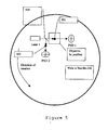
- a single laser is used and a 50/50 mirror 504 oriented at a compound angle directs a second beam onto the surface to a position labeled 502 on figure 5 .
- the beam that passes through the 50/50 mirror 504 is directed onto the surface to a position labeled 501 on figure 5 .
- the entire surface of the object to be measured is scanned with both of the beams resulting in at least two images of the surface.
- the resulting images are stored and digitally shifted so that the resulting images have the object to be profiled at the same x, y location.
- the resulting shifted images may then be subtracted to give the height profile in the manner described above.
- the advantage of this embodiment is that it uses only a single laser and fewer optical components and the beam shape of the two beams is identical.
- Laser one and PSD 1 nominally measure the signal in the radial, Sr, and the signal in the circumferential, Sc, directions. However, the nature of the PSD results in Sc from laser one and PSD 1 being contaminated with height information, in addition to slope information. Sr from laser 1 and PSD 1 include only slope information. Laser two and PSD 2 also nominally measure the slope in the radial and circumferential directions. However, Sr from laser 2 and PSD 2 measures both slope and height at the same positions as Sr from laser 1 and PSD 1. As a result the true height variation can be obtained by subtracting Sr from laser 2 and PSD 2 from Sr from laser 1 and PSD 1. That is, the slope information is removed when subtracting Sr from PSD 2 from Sr from PSD 1, leaving only the height information.
- Figure 6 shows the side view design of the optical profilometer. This figure only shows laser 1 and PSD 1 in an effort to easily show the side view design.
- the optical profilometer is positioned above a thin film disk or wafer and is translated in the radial direction while the disk or semiconductor wafer is rotated.
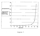
- the angle of incidence ( ⁇ ) shown in Figure 6 can be chosen for the particular application. Any angle of incidence can be chosen except normal incidence, where the PSD's would have no height sensitivity. For an application that involves transparent substrates one could choose angles greater than 45 degrees in order to increase the reflection signal from the surface. As the angle of incidence increases, the height sensitivity also increases by the factor sin ( ⁇ ) /cos 2 ( ⁇ ). A plot of this factor is shown in Figure 7 . This suggests that an angle of incidence greater than or equal to approximately 60 degrees would be optimal, although not necessary. At angles greater than 60 degrees the sensitivity will increase and the signal from a transparent surface will increase. This invention requires that the focused spot sizes of the two lasers be substantially identical and that the laser spots overlap as closely as possible.
- a problem in the magnetic recording industry is to inspect thin film disks for defects at the final test step of the manufacturer of disks.
- the manufacturers of thin film disks require that both sides of the thin film disk be inspected simultaneously.
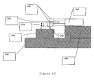
- the problem is that the clearance between the disk and the chuck (which holds the disk) is only 2.54 cm (1'') or less (see Figure 13 , 1304).
- This requires that the optics be miniaturized in order to fit in the small space between the disk and the chuck (see figure 13 ).
- a solution to this problem can be obtained by using the optical designs in Figure 8 , 9 , 10 , and 11 . These designs have several key improvements over conventional systems, which allow the design to be miniaturized without compromising the performance of the device.
- the design uses the internal feedback photodiode, which is contained within the laser diode 801, to achieve stabilization of the DC level of the optical signal.
- the angle of incidence, ⁇ is adjusted to reduce the height of the instrument so that it will fit within the 2.54 cm (1'') space requirement.
- the surface topography measurement capability feature of the instrument is incorporated within the phase/specular detectors 808 and 809 shown in Figures 8 and 9 .
- the position sensitive detectors 808 and 809 serve as both phase detectors, specular detectors, and topography measurement detectors.
- the size may be decreased by using a polarizing beam splitter 901 as shown in Figure 9 instead of a Wollaston prism 807 as shown in Figure 8 .
- the polarizing beam splitter 807 or Wollaston prism 901 is rotated at 45° with respect to the plane of incidence.
- Another embodiment of this invention can use a beam splitter that splits the beam into non-orthogonal components, which will be discussed in a subsequent section.
- Fifthly using two spherical mirrors 1004 and 1006 to direct the beam onto the disk as shown in Figure 10 will diminish the size in the lateral dimension.
- the mirrors 1004 and 1006 are adjusted at a compound angle as shown in Figures 10 .
- FIG 11 is a view of Figure 10 along the "A" direction, where the mirrors that are at a compound angle are 1102 and 1104. These mirrors direct the beam 1103 onto the disk or wafer 1101. In addition to directing the beam onto the disk the spherical mirrors also focus the beam to a small spot.
- An alternative embodiment to the use of a spherical mirror is to use flat mirrors 1202 and 1203 in combination with focussing lenses 1201 as shown in Figure 12 .
- a silicon photodetector or avalanche photodiode 1204 which is positioned above the point where the beam strikes the disk. This element enables the detection of submicron particles.
- the avalanche photodiode 1204 is available from Advanced Photonix, Inc., Camarillo, CA.
- the laser beam from the diode laser 801 passes through a linear polarizer 802, and a focussing lens 803 and then strikes a disk or wafer 804.
- the beam Upon reflecting from the surface the beam passes through a recollimating lens 805, a quarter wave plate 806, and through a polarizing beam splitter such as Wollaston prism 807 which is rotated at 45° to the plane of incidence and onto two quadrant detectors 808 and 809.
- SCD B ⁇ 1 + C ⁇ 1 - A ⁇ 1 + D ⁇ 1 / ( A ⁇ 1 + B ⁇ 1 + C ⁇ 1 + D ⁇ 1 )
- SRD A ⁇ 1 + B ⁇ 1 - C ⁇ 1 + D ⁇ 1 / ( A ⁇ 1 + B ⁇ 1 + C ⁇ 1 + D ⁇ 1 )
- the topography in the circumferential or radial direction is obtained by integrating the slope in the circumferential or radial direction, respectively.
- the slope signals can also be obtained from detector 2, 808 with the same equations as shown above except for substituting 2 for 1.
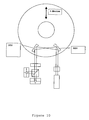
- FIG. 13 One embodiment of a miniature optical design that may be mounted on the top and bottom of a thin film disk 1302 is shown in Figure 13 .
- the resulting combination is translated over the surface of the disk with a stepper or DC servomotor driven stage 1308.
- a spindle motor 1306 rotates the disk while the optics 1301 is translated in the radial direction so that 100% of the surface of the disk may be measured for defects.
- the entire apparatus is mounted on a baseplate 1307.
- the electronics package is located above the stepper motor 1303.
- the disk is placed upon a vacuum chuck 1305 that is rotated at a high rate of speed.
- a problem in the inspection of transparent glass substrates 1406 and other transparent objects is to separate the signal from the top and the bottom surface. This can be accomplished by the use of a spatial filter 1404 that blocks the signal from the bottom surface 1405 and does not affect the top surface reflection 1403.
- Figure 14 shows this in the optical design of an Optical Surface Analyzer (OSA).
- the incoming optical beam is 1401.
- the spatial filter 1404 is in the shape of a small wedge that is attached to the bottom surface of an integrating sphere 1402.
- the location of the spatial filter is adjusted to just block the bottom surface reflection 1405 and not to interfere with the top surface reflection 1403.
- This invention allows one to separate information from the top and bottom surface of a transparent glass disk or wafer 1406.
- This invention also works with any transparent medium such as lithium niobate, fused silica, photoresist, and other transparent oxides.
- an alternative design does not require the spatial filter to be attached to the bottom of the integrating sphere.
- the integrating sphere may be omitted and the spatial filter may be attached to any other point on the optical body.
- the spatial filter should be located near enough to the transparent substrate so that the reflections from the top and bottom surface are separated in the lateral plane. In this manner it is possible to intercept the bottom surface reflection with the spatial filter and leave the top surface reflection unaffected.
- a problem in the measurement of semiconductor wafers is the detection of defects caused by the CMP (Chemical Mechanical Polishing) process. These defects can be residual copper, nitride, slurry, particles, scratches and stains.
- the measurement is complicated by the fact that the semiconductor wafers have a complex pattern on their surface.
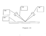
- a goal is to separate the defects from the complex pattern of semiconductor devices on the surface of the semiconductor wafer. This can be accomplished by the design shown in Figure 15 .
- the device consists of a means for measuring the phase shift between the P and S polarization components of the incident beam and a means to measure the topography of the surface.
- the device consists of a laser 1501 and a polarizer 1502.
- the laser is directed onto a focussing lens 1503 and onto a mirror 1504 that directs the beam onto a wafer or disk 1505 that may be rotated by a motor 1506.
- the reflected beam is directed by another mirror 1507 onto a collimating lens 1508 and through a quarter wave plate 1509.
- the signal passing through the quarter wave plate is directed onto a polarizing beam splitter 1511 that is oriented at 45° to the plane of incidence.
- the split beams are measured with two photodetectors 1510 and 1512.
- the phase shift of the incident beam is proportional to the difference in the amplitudes of photodetectors 1510 and 1512.
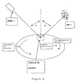
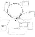
- a means to accomplish this is to image the wafer with two orthogonal beams as shown in Figure 16 .
- An optical path shown in Figure 15 generates each of the beams shown in Figure 16 .
- Laser one 1601 and detector one 1602 in Figure 16 generate a phase shift image of the surface that has one particular amplitude due to the orientation of the semiconductor pattern lines.
- Laser two 1603 and detector two 1604 have a particular amplitude pattern that is identical in lateral shape but opposite in amplitude to that generated by laser one 1601 and detector one 1602. This is because the orientation of the optical beams of lasers one and two are orthogonal with respect to the orientation of the pattern lines.
- what is generated are two phase shift images of the surface of the semiconductor that have opposite amplitude phase shift signals from the semiconductor pattern lines. If these two images are added together then the semiconductor pattern will be greatly attenuated.
- Defects on the other hand, do not change phase shift in the two orthogonal beams and as a result when the two orthogonal images are added the defects increase in amplitude and the semiconductor pattern diminishes in amplitude. Defects do not have opposite phase shift amplitudes since most defects are isotropic in nature and do not have the strong anisotropy associated with semiconductor pattern lines. This technique effectively enhances the defect signals and diminishes the semiconductor pattern signal.
- the focussed beams 1607 cross at point 1606. The entire device is contained within housing 1605.
- This invention has the additional advantage that it can simultaneously measure the topography of the surface.
- the angle of incidence ( ⁇ ) shown in Figure 15 is at approximately 60°. Larger or smaller angles of incidence may be used depending upon the application. For example, a larger angle of incidence may be used if a transparent substrate is to be examined. This would be advantageous since a transparent substrate will give a larger signal from the top surface with a greater angle of incidence.
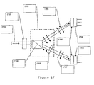
- Figure 17 illustrates the measurement of the phase shift of an elliptically polarized beam by the use of a beam splitter that splits the beam into non-orthogonally polarized components which is not an embodiment of the present invention.
- the incoming elliptically polarized beam is labeled 1701, this beam is directed into a quarter wave plate 1702 and subsequently into a beam splitter 1703 which splits the beam into non-orthogonally polarized components.
- a polarizing beam splitter such as a Wollaston prism 1704 or a polarizing cube beam splitter and a polarization rotation device 1705 such as a half wave plate or an optically active quartz polarization rotator.
- the two beams leaving the beam splitter 1703 are polarized in the same direction as indicated by 1706 and 1707.
- the two beams leaving the beam splitter 1703 may be polarized at any angle with respect to the other. This is accomplished by rotating a half wave plate 1705 (which is internal to the beam splitter 1703) to an arbitrary angle so that the beam leaving 1707 will now be polarized at an arbitrary angle with respect to beam 1706.
- the advantage of this type of beam splitter 1703 is that the outgoing beams may be polarized in the same direction.
- the incoming laser beams discussed in previous paragraphs have been described as P, S or 45° polarized beams. These earlier discussions are preferred embodiments of this invention. It is also possible to illuminate the surface with unpolarized light and detect the resulting reflected signals with the same optical and electronic methods. The resulting detected signals, which use a source of light which is unpolarized, will still give measurements of the phase shift, topography, reflectivity, defects and particles.
Landscapes
- Physics & Mathematics (AREA)
- General Physics & Mathematics (AREA)
- Length Measuring Devices By Optical Means (AREA)
- Investigating Materials By The Use Of Optical Means Adapted For Particular Applications (AREA)
- Manufacturing Of Magnetic Record Carriers (AREA)
- Optical Radar Systems And Details Thereof (AREA)
Applications Claiming Priority (4)
| Application Number | Priority Date | Filing Date | Title |
|---|---|---|---|
| US861280 | 1986-05-09 | ||
| US818199 | 1997-03-14 | ||
| US09/818,199 US20020015146A1 (en) | 1997-09-22 | 2001-03-26 | Combined high speed optical profilometer and ellipsometer |
| US09/861,280 US6757056B1 (en) | 2001-03-26 | 2001-05-18 | Combined high speed optical profilometer and ellipsometer |
Publications (2)
| Publication Number | Publication Date |
|---|---|
| EP1245922A1 EP1245922A1 (en) | 2002-10-02 |
| EP1245922B1 true EP1245922B1 (en) | 2010-05-12 |
Family
ID=27124244
Family Applications (1)
| Application Number | Title | Priority Date | Filing Date |
|---|---|---|---|
| EP02006807A Expired - Lifetime EP1245922B1 (en) | 2001-03-26 | 2002-03-25 | System for measuring phase differences in reflected light signals |
Country Status (4)
| Country | Link |
|---|---|
| EP (1) | EP1245922B1 (enExample) |
| JP (1) | JP4008730B2 (enExample) |
| AT (1) | ATE467810T1 (enExample) |
| DE (1) | DE60236337D1 (enExample) |
Cited By (1)
| Publication number | Priority date | Publication date | Assignee | Title |
|---|---|---|---|---|
| TWI879585B (zh) * | 2023-09-20 | 2025-04-01 | 日商斯庫林集團股份有限公司 | 觀察裝置、觀察方法以及基板處理裝置 |
Families Citing this family (12)
| Publication number | Priority date | Publication date | Assignee | Title |
|---|---|---|---|---|
| US6798512B2 (en) | 2001-08-09 | 2004-09-28 | Therma-Wave, Inc. | Multiple beam ellipsometer |
| US7224471B2 (en) * | 2003-10-28 | 2007-05-29 | Timbre Technologies, Inc. | Azimuthal scanning of a structure formed on a semiconductor wafer |
| SE0303048L (sv) * | 2003-11-17 | 2004-12-28 | Optonova Ab | Förfarande och anordning för beröringsfri avsyning och inmätning av ytegenskaper och ytdefekter på en materialyta |
| JP4748353B2 (ja) * | 2005-08-04 | 2011-08-17 | 大日本印刷株式会社 | 異物検査装置 |
| DE102007043937B4 (de) * | 2006-09-13 | 2010-10-07 | Innovent E.V. | Verfahren zur Bestimmung der Dicke und des Brechungsindex von optisch transparenten Schichten auf optisch transparenten planparallelen Substraten |
| SG152187A1 (en) * | 2007-10-25 | 2009-05-29 | Asml Netherlands Bv | Inspection method and apparatus, lithographic apparatus, lithographic processing cell and device manufacturing method |
| CN102192882B (zh) * | 2011-03-11 | 2013-01-09 | 山东大学 | 利用锁相放大器进行磁光椭偏测量的测量方法 |
| US12416580B2 (en) | 2018-05-07 | 2025-09-16 | Unm Rainforest Innovations | Method and system for in-line optical scatterometry |
| US11473901B2 (en) | 2018-05-29 | 2022-10-18 | Hitachi High-Tech Corporation | Height measurement device in which optical paths projected on the sample at different incidence angles |
| US11043239B2 (en) * | 2019-03-20 | 2021-06-22 | Kla Corporation | Magneto-optic Kerr effect metrology systems |
| WO2021087345A1 (en) * | 2019-11-01 | 2021-05-06 | Unm Rainforest Innovations | In-line angular optical multi-point scatterometry for nanomanufacturing systems |
| CN115388765B (zh) * | 2022-08-10 | 2023-10-24 | 睿励科学仪器(上海)有限公司 | 用于椭偏量测系统的自动聚焦装置 |
Citations (1)
| Publication number | Priority date | Publication date | Assignee | Title |
|---|---|---|---|---|
| US4906844A (en) * | 1988-08-12 | 1990-03-06 | Rockwell International Corporation | Phase sensitive optical monitor for thin film deposition |
Family Cites Families (8)
| Publication number | Priority date | Publication date | Assignee | Title |
|---|---|---|---|---|
| US4585348A (en) * | 1981-09-28 | 1986-04-29 | International Business Machines Corporation | Ultra-fast photometric instrument |
| US4674875A (en) | 1983-12-09 | 1987-06-23 | Hitachi, Ltd. | Method and apparatus for inspecting surface defects on the magnetic disk file memories |
| JP3140664B2 (ja) | 1995-06-30 | 2001-03-05 | 松下電器産業株式会社 | 異物検査方法及び装置 |
| US5694214A (en) | 1996-01-08 | 1997-12-02 | Hitachi Electronics Engineering Co., Ltd. | Surface inspection method and apparatus |
| NL1006016C2 (nl) * | 1997-05-09 | 1998-11-10 | Univ Delft Tech | Ellipsometer met twee lasers. |
| JPH112512A (ja) | 1997-06-11 | 1999-01-06 | Super Silicon Kenkyusho:Kk | ウェーハの光学式形状測定器 |
| US6134011A (en) | 1997-09-22 | 2000-10-17 | Hdi Instrumentation | Optical measurement system using polarized light |
| US6157444A (en) | 1997-11-28 | 2000-12-05 | Hitachi, Ltd. | Defect inspection apparatus for silicon wafer |
-
2002
- 2002-03-25 AT AT02006807T patent/ATE467810T1/de not_active IP Right Cessation
- 2002-03-25 DE DE60236337T patent/DE60236337D1/de not_active Expired - Lifetime
- 2002-03-25 EP EP02006807A patent/EP1245922B1/en not_active Expired - Lifetime
- 2002-03-26 JP JP2002085531A patent/JP4008730B2/ja not_active Expired - Lifetime
Patent Citations (1)
| Publication number | Priority date | Publication date | Assignee | Title |
|---|---|---|---|---|
| US4906844A (en) * | 1988-08-12 | 1990-03-06 | Rockwell International Corporation | Phase sensitive optical monitor for thin film deposition |
Cited By (1)
| Publication number | Priority date | Publication date | Assignee | Title |
|---|---|---|---|---|
| TWI879585B (zh) * | 2023-09-20 | 2025-04-01 | 日商斯庫林集團股份有限公司 | 觀察裝置、觀察方法以及基板處理裝置 |
Also Published As
| Publication number | Publication date |
|---|---|
| ATE467810T1 (de) | 2010-05-15 |
| DE60236337D1 (de) | 2010-06-24 |
| EP1245922A1 (en) | 2002-10-02 |
| JP2002365232A (ja) | 2002-12-18 |
| JP4008730B2 (ja) | 2007-11-14 |
Similar Documents
| Publication | Publication Date | Title |
|---|---|---|
| US7075630B2 (en) | Combined high speed optical profilometer and ellipsometer | |
| US6897957B2 (en) | Material independent optical profilometer | |
| US7362425B2 (en) | Wide spatial frequency topography and roughness measurement | |
| US7061601B2 (en) | System and method for double sided optical inspection of thin film disks or wafers | |
| US6909500B2 (en) | Method of detecting and classifying scratches, particles and pits on thin film disks or wafers | |
| US7123357B2 (en) | Method of detecting and classifying scratches and particles on thin film disks or wafers | |
| US6930765B2 (en) | Multiple spot size optical profilometer, ellipsometer, reflectometer and scatterometer | |
| US6392749B1 (en) | High speed optical profilometer for measuring surface height variation | |
| US6956658B2 (en) | System and method for measuring object characteristics using phase differences in polarized light reflections | |
| US7630086B2 (en) | Surface finish roughness measurement | |
| US6956660B2 (en) | System and method for measuring properties of an object using a phase difference between two reflected light signals | |
| US20020015146A1 (en) | Combined high speed optical profilometer and ellipsometer | |
| US7714995B2 (en) | Material independent profiler | |
| US6307627B1 (en) | Optical measurement system using polarized light | |
| EP1245922B1 (en) | System for measuring phase differences in reflected light signals | |
| US7345751B2 (en) | Material independent optical profilometer | |
| US6882437B2 (en) | Method of detecting the thickness of thin film disks or wafers |
Legal Events
| Date | Code | Title | Description |
|---|---|---|---|
| PUAI | Public reference made under article 153(3) epc to a published international application that has entered the european phase |
Free format text: ORIGINAL CODE: 0009012 |
|
| AK | Designated contracting states |
Kind code of ref document: A1 Designated state(s): AT BE CH CY DE DK ES FI FR GB GR IE IT LI LU MC NL PT SE TR |
|
| AX | Request for extension of the european patent |
Free format text: AL;LT;LV;MK;RO;SI |
|
| 17P | Request for examination filed |
Effective date: 20030304 |
|
| AKX | Designation fees paid |
Designated state(s): AT BE CH CY DE DK ES FI FR GB GR IE IT LI LU MC NL PT SE TR |
|
| 17Q | First examination report despatched |
Effective date: 20050613 |
|
| GRAC | Information related to communication of intention to grant a patent modified |
Free format text: ORIGINAL CODE: EPIDOSCIGR1 |
|
| GRAP | Despatch of communication of intention to grant a patent |
Free format text: ORIGINAL CODE: EPIDOSNIGR1 |
|
| RTI1 | Title (correction) |
Free format text: SYSTEM FOR MEASURING PHASE DIFFERENCES IN REFLECTED LIGHT SIGNALS |
|
| GRAS | Grant fee paid |
Free format text: ORIGINAL CODE: EPIDOSNIGR3 |
|
| GRAA | (expected) grant |
Free format text: ORIGINAL CODE: 0009210 |
|
| AK | Designated contracting states |
Kind code of ref document: B1 Designated state(s): AT BE CH CY DE DK ES FI FR GB GR IE IT LI LU MC NL PT SE TR |
|
| REG | Reference to a national code |
Ref country code: GB Ref legal event code: FG4D |
|
| REG | Reference to a national code |
Ref country code: CH Ref legal event code: EP |
|
| REG | Reference to a national code |
Ref country code: NL Ref legal event code: T3 |
|
| REG | Reference to a national code |
Ref country code: IE Ref legal event code: FG4D |
|
| REF | Corresponds to: |
Ref document number: 60236337 Country of ref document: DE Date of ref document: 20100624 Kind code of ref document: P |
|
| PG25 | Lapsed in a contracting state [announced via postgrant information from national office to epo] |
Ref country code: ES Free format text: LAPSE BECAUSE OF FAILURE TO SUBMIT A TRANSLATION OF THE DESCRIPTION OR TO PAY THE FEE WITHIN THE PRESCRIBED TIME-LIMIT Effective date: 20100823 Ref country code: SE Free format text: LAPSE BECAUSE OF FAILURE TO SUBMIT A TRANSLATION OF THE DESCRIPTION OR TO PAY THE FEE WITHIN THE PRESCRIBED TIME-LIMIT Effective date: 20100512 |
|
| PG25 | Lapsed in a contracting state [announced via postgrant information from national office to epo] |
Ref country code: AT Free format text: LAPSE BECAUSE OF FAILURE TO SUBMIT A TRANSLATION OF THE DESCRIPTION OR TO PAY THE FEE WITHIN THE PRESCRIBED TIME-LIMIT Effective date: 20100512 Ref country code: FI Free format text: LAPSE BECAUSE OF FAILURE TO SUBMIT A TRANSLATION OF THE DESCRIPTION OR TO PAY THE FEE WITHIN THE PRESCRIBED TIME-LIMIT Effective date: 20100512 |
|
| PG25 | Lapsed in a contracting state [announced via postgrant information from national office to epo] |
Ref country code: GR Free format text: LAPSE BECAUSE OF FAILURE TO SUBMIT A TRANSLATION OF THE DESCRIPTION OR TO PAY THE FEE WITHIN THE PRESCRIBED TIME-LIMIT Effective date: 20100813 Ref country code: CY Free format text: LAPSE BECAUSE OF FAILURE TO SUBMIT A TRANSLATION OF THE DESCRIPTION OR TO PAY THE FEE WITHIN THE PRESCRIBED TIME-LIMIT Effective date: 20100512 |
|
| PG25 | Lapsed in a contracting state [announced via postgrant information from national office to epo] |
Ref country code: PT Free format text: LAPSE BECAUSE OF FAILURE TO SUBMIT A TRANSLATION OF THE DESCRIPTION OR TO PAY THE FEE WITHIN THE PRESCRIBED TIME-LIMIT Effective date: 20100913 Ref country code: DK Free format text: LAPSE BECAUSE OF FAILURE TO SUBMIT A TRANSLATION OF THE DESCRIPTION OR TO PAY THE FEE WITHIN THE PRESCRIBED TIME-LIMIT Effective date: 20100512 |
|
| PG25 | Lapsed in a contracting state [announced via postgrant information from national office to epo] |
Ref country code: BE Free format text: LAPSE BECAUSE OF FAILURE TO SUBMIT A TRANSLATION OF THE DESCRIPTION OR TO PAY THE FEE WITHIN THE PRESCRIBED TIME-LIMIT Effective date: 20100512 |
|
| PLBE | No opposition filed within time limit |
Free format text: ORIGINAL CODE: 0009261 |
|
| STAA | Information on the status of an ep patent application or granted ep patent |
Free format text: STATUS: NO OPPOSITION FILED WITHIN TIME LIMIT |
|
| PG25 | Lapsed in a contracting state [announced via postgrant information from national office to epo] |
Ref country code: IT Free format text: LAPSE BECAUSE OF FAILURE TO SUBMIT A TRANSLATION OF THE DESCRIPTION OR TO PAY THE FEE WITHIN THE PRESCRIBED TIME-LIMIT Effective date: 20100512 |
|
| 26N | No opposition filed |
Effective date: 20110215 |
|
| REG | Reference to a national code |
Ref country code: DE Ref legal event code: R097 Ref document number: 60236337 Country of ref document: DE Effective date: 20110214 |
|
| PG25 | Lapsed in a contracting state [announced via postgrant information from national office to epo] |
Ref country code: MC Free format text: LAPSE BECAUSE OF NON-PAYMENT OF DUE FEES Effective date: 20110331 |
|
| REG | Reference to a national code |
Ref country code: CH Ref legal event code: PL |
|
| REG | Reference to a national code |
Ref country code: FR Ref legal event code: ST Effective date: 20111130 |
|
| REG | Reference to a national code |
Ref country code: IE Ref legal event code: MM4A |
|
| PG25 | Lapsed in a contracting state [announced via postgrant information from national office to epo] |
Ref country code: IE Free format text: LAPSE BECAUSE OF NON-PAYMENT OF DUE FEES Effective date: 20110325 Ref country code: FR Free format text: LAPSE BECAUSE OF NON-PAYMENT OF DUE FEES Effective date: 20110331 Ref country code: CH Free format text: LAPSE BECAUSE OF NON-PAYMENT OF DUE FEES Effective date: 20110331 Ref country code: LI Free format text: LAPSE BECAUSE OF NON-PAYMENT OF DUE FEES Effective date: 20110331 |
|
| PG25 | Lapsed in a contracting state [announced via postgrant information from national office to epo] |
Ref country code: LU Free format text: LAPSE BECAUSE OF NON-PAYMENT OF DUE FEES Effective date: 20110325 |
|
| PG25 | Lapsed in a contracting state [announced via postgrant information from national office to epo] |
Ref country code: TR Free format text: LAPSE BECAUSE OF FAILURE TO SUBMIT A TRANSLATION OF THE DESCRIPTION OR TO PAY THE FEE WITHIN THE PRESCRIBED TIME-LIMIT Effective date: 20100512 |
|
| PGFP | Annual fee paid to national office [announced via postgrant information from national office to epo] |
Ref country code: DE Payment date: 20150327 Year of fee payment: 14 Ref country code: NL Payment date: 20150326 Year of fee payment: 14 |
|
| PGFP | Annual fee paid to national office [announced via postgrant information from national office to epo] |
Ref country code: GB Payment date: 20150327 Year of fee payment: 14 |
|
| REG | Reference to a national code |
Ref country code: DE Ref legal event code: R119 Ref document number: 60236337 Country of ref document: DE |
|
| REG | Reference to a national code |
Ref country code: NL Ref legal event code: MM Effective date: 20160401 |
|
| GBPC | Gb: european patent ceased through non-payment of renewal fee |
Effective date: 20160325 |
|
| PG25 | Lapsed in a contracting state [announced via postgrant information from national office to epo] |
Ref country code: GB Free format text: LAPSE BECAUSE OF NON-PAYMENT OF DUE FEES Effective date: 20160325 Ref country code: NL Free format text: LAPSE BECAUSE OF NON-PAYMENT OF DUE FEES Effective date: 20160401 Ref country code: DE Free format text: LAPSE BECAUSE OF NON-PAYMENT OF DUE FEES Effective date: 20161001 |
|
| P01 | Opt-out of the competence of the unified patent court (upc) registered |
Effective date: 20230525 |