EP1242891B1 - Partitionierte speichervorrichtung mit merkmalen unterschiedlicher speichertechnologien - Google Patents
Partitionierte speichervorrichtung mit merkmalen unterschiedlicher speichertechnologien Download PDFInfo
- Publication number
- EP1242891B1 EP1242891B1 EP00984535A EP00984535A EP1242891B1 EP 1242891 B1 EP1242891 B1 EP 1242891B1 EP 00984535 A EP00984535 A EP 00984535A EP 00984535 A EP00984535 A EP 00984535A EP 1242891 B1 EP1242891 B1 EP 1242891B1
- Authority
- EP
- European Patent Office
- Prior art keywords
- memory
- management unit
- volatile
- application
- processing circuit
- Prior art date
- Legal status (The legal status is an assumption and is not a legal conclusion. Google has not performed a legal analysis and makes no representation as to the accuracy of the status listed.)
- Expired - Lifetime
Links
Images


Classifications
-
- G—PHYSICS
- G06—COMPUTING OR CALCULATING; COUNTING
- G06F—ELECTRIC DIGITAL DATA PROCESSING
- G06F12/00—Accessing, addressing or allocating within memory systems or architectures
- G06F12/02—Addressing or allocation; Relocation
-
- G—PHYSICS
- G06—COMPUTING OR CALCULATING; COUNTING
- G06F—ELECTRIC DIGITAL DATA PROCESSING
- G06F12/00—Accessing, addressing or allocating within memory systems or architectures
- G06F12/14—Protection against unauthorised use of memory or access to memory
- G06F12/1416—Protection against unauthorised use of memory or access to memory by checking the object accessibility, e.g. type of access defined by the memory independently of subject rights
- G06F12/145—Protection against unauthorised use of memory or access to memory by checking the object accessibility, e.g. type of access defined by the memory independently of subject rights the protection being virtual, e.g. for virtual blocks or segments before a translation mechanism
Definitions
- the present invention relates generally to a memory management system for single-chip data processing circuits, such as a smart card, and more particularly, to a memory management method and apparatus that (i) partitions homogeneous memory devices to achieve heterogeneous memory characteristics and (ii) restricts access of installed applications to predetermined memory ranges.
- Smart cards typically contain a central processing unit (CPU) or a microprocessor to control all processes and transactions associated with the smart card.
- the microprocessor is used to increase the security of the device, by providing a flexible method to implement complex and variable algorithms that ensure integrity and access to data stored in non volatile memory.
- smart cards contain non-volatile memory, for storing program code and changed data, and volatile memory for the temporary storage of certain information. In conventional smart cards, each memory type has been implemented using different technologies.
- Byte erasable EEPROM for example, is typically used to store non-volatile data, that changes or configures the device in the field, while Masked-Rom and more recently one-time-programmable read-only memory (OTPROM) is typically used to store program code.
- OTPROM one-time-programmable read-only memory
- Volatile memory is normally implemented as random access memory (RAM).
- RAM random access memory
- the hardware technologies associated with each memory type provide desirable security benefits. For example, the one-time nature of OTPROM prevents authorized program code from being modified or over-written with unauthorized program code. Likewise, the implementation of volatile memory as RAM ensures that the temporarily stored information, such as an encryption key, is cleared after each use.
- FERAM ferroelectric random access memory
- FERAM ferroelectric random access memory
- FERAM is a nonvolatile memory employing a ferroelectric material to smart cards.
- FERAM is a nonvolatile memory employing a ferroelectric material to store the information based on the polarization state of the ferroelectric material.
- Such homogeneous memory devices are desirable since they are non-volatile, while providing the speed of RAM, and the density of ROM while using little energy.
- the homogeneous nature of such memory devices eliminates the security benefits that were previously provided by the various hardware technologies themselves. Thus, a need exists for the ability to partition such otherwise homogeneous memory devices into volatile, non-volatile and program storage (ROM) regions with the appropriate corresponding memory characteristics.
- United States Patent Number 5,912,453 discloses the integration of multiple application programs on one chip card, whereby the application programs stored on it do not have access to each other, which is achieved through a separation and de-coupling of the individual programs from one another.
- United States Patent Number 5,890,199 to Downs discloses a system for selectively configuring a homogeneous memory, such as FERAM, as read/write memory, read only memory (ROM) or a combination of the foregoing.
- a homogeneous memory such as FERAM
- ROM read only memory
- the Downs system allows a single portion of the memory array to be partitioned as ROM for storing the software code for only an application.
- the Downs system does not provide a mechanism for configuring the homogeneous memory to behave like RAM that provides for the temporary storage of information that is cleared after each use.
- Single-chip microprocessors such as those used in smart cards, increasingly support multiple functions (applications) and must be able to download an application for immediate execution in support of a given function.
- a system would allow a third party to create an application and load it onto a standard card, which removes the control over the integrity of the software allowing malicious attacks.
- This may be overcome, for example, by programming an interpreter into the card that indirectly executes a command sequence (as opposed to the micrprocessor executing a binary directly).
- This technique requires more processing power for a given function and additional code on the device which further increases the cost of a cost-sensitive product.
- a mechanism is required that ensures that every memory transaction made by a loaded application is limited to the memory areas allocated to it. Furthermore, this mechanism needs to function independently of the software such that it cannot be altered by malicious programs. Thus, even malicious software is controlled.
- Hardware-implementations of an access control mechanism will maximize the security of the single-chip microprocessor, and allow code to be reused, by isolating the code from the actual hardware implementation of the device.
- a hardware-implemented access control mechanism allows a secure kernel (operating system) to be embedded into the device, having access rights to features of the device that are denied to applications.
- the present invention concerns a single-chip data processing circuit according to claim 1 and a method for partitioning a homogeneous memory device according to claim 10.
- a memory management unit for a single-chip data processing circuit, such as a smart card.
- the memory management unit (i) partitions a homogeneous memory device to achieve heterogeneous memory characteristics for various regions of the memory device, and (ii) restricts access of installed applications executing in the microprocessor core to predetermined memory ranges.
- the memory management unit imposes firewalls between applications and permits hardware checked partitioning of the memory.
- the memory management unit provides two operating modes for the processing circuit.
- a secure kernel mode the programmer can access all resources of the device including hardware control.
- an application mode the memory management unit translates the virtual memory address used by the software creator into the physical address allocated to the application by the operating system in a secure kernel mode during installation.
- the present invention also ensures that an application does not access memory outside of the memory mapped to the application by the software when in secure kernel mode. Any illegal memory accesses attempted by an application will cause a trap, and in one embodiment, the memory management unit restarts the microprocessor in a secure kernel mode, optionally setting flags to permit a system programmer to implement an appropriate mechanism to deal with the exception.
- An application table records the memory demands of each application that is installed on the single-chip data processing circuit, such as the volatile, non-volatile and program storage (OTPROM) memory requirements of each application.
- the memory management unit implements memory address checking using limit registers and translates virtual addresses to an absolute memory address using offset registers. Once the appropriate memory areas have been allocated to each application program, the memory management unit loads limit and offset registers with the appropriate values from the application table to ensure that the executing application only accesses the designated memory locations.
- the memory management unit partitions a homogeneous memory device, such as an FERAM memory device, to achieve heterogeneous memory characteristics normally associated with a plurality of memory technologies, such as volatile, non-volatile and program storage (ROM) memory segments.
- a homogeneous memory device such as an FERAM memory device
- ROM volatile, non-volatile and program storage
- the memory management unit enforces the appropriate corresponding memory characteristics for each heterogeneous memory type.
- a memory partition control logic is programmed with the required partitioning associated with each portion of the homogeneous memory in order that the homogenous memory behaves like volatile, non-volatile and program storage (OTPROM) memory technologies, as desired.
- FIG. 1 illustrates a single-chip data processing circuit 100, such as a smart card, that includes a microprocessor core 110, memory devices 120, 130 and a memory management unit 200 that interfaces between the microprocessor core 110 and the memory devices 120, 130 for memory access operations.
- the memory management unit 200 (i) partitions a homogeneous memory device to achieve heterogeneous memory characteristics for various regions of the memory device, and (ii) restricts access of installed applications executing in the microprocessor core 110 to predetermined memory ranges. It is noted that each of these two features are independent, and may be selectively and separately implemented in the memory management unit 200, as would be apparent to a person of ordinary skill.
- the present invention is illustrated in a smart card environment, the present invention applies to any single-chip data processing circuit, as would be apparent to a person of ordinary skill in the art.
- the memory management unit 200 imposes firewalls between applications and thereby permits hardware checked partitioning of the memory.
- an application has limited access to only a predetermined memory range.
- the memory management unit 200 performs memory address checking and translates addresses based on user-specified criteria.
- the memory management unit 200 provides two operating modes for the microprocessor 110.
- a secure kernel mode the programmer can access all resources of the device including hardware control.
- an application mode the memory management unit 200 translates the virtual memory address used by the software creator into the physical address allocated to the application by the operating system in a secure kernel mode during installation.
- the present invention also ensures that an application does not access memory outside of the memory mapped to the application by the software when in secure kernel mode. Any illegal memory accesses attempted by an application will cause a trap, and in one embodiment, the memory management unit 200 restarts the microprocessor 110 in a secure kernel mode, optionally setting flags to permit a system programmer to implement an appropriate mechanism to deal with the exception.
- an exception is identified if an application is written with the accidental or specific intention of compromising the security of the smart card, by accessing stored data, code or by manipulating the hardware to indirectly influence the operation of the chip.
- the memory management unit 200 limits the application to the allocated program code and data areas. Any other references result in termination of the application and flagging the secure kernel that such an illegal attempt has been made.
- each application is isolated from all other applications, the hardware and the secure kernel.
- the security mechanism acts as a general protection unit trapping software errors.
- the memory management unit 200 partitions a homogeneous memory device, such as an FERAM memory device, to achieve heterogeneous memory characteristics normally associated with a plurality of memory technologies, such as volatile, non-volatile and program storage (ROM) memory segments. Once partitioned, the memory management unit 200 enforces the appropriate corresponding memory characteristics for each heterogeneous memory type.
- a homogeneous memory device such as an FERAM memory device
- ROM program storage
- FIG. 2 provides a schematic block diagram of an exemplary hardware-implementation of the memory management unit 200.
- the memory management unit 200 partitions a homogeneous memory device to achieve heterogeneous memory characteristics for various regions of the memory device, and (ii) restricts access of installed applications executing in the microprocessor core 110 to predetermined memory ranges.
- the memory management unit 200 includes a section for memory partition control logic 400.
- the memory partition control logic 400 is programmed with the required partitioning associated with each portion of the homogeneous memory in order that the homogenous memory behaves like volatile, non-volatile and program storage (OTPROM) memory technologies, as desired.
- OTPROM volatile, non-volatile and program storage
- An application would normally be allocated different memory areas for code and data, and the data area can be further divided into a volatile portion, for scratchpad operations, and non-volatile storage areas.
- the memory management unit 200 includes an application table 300, discussed further below in conjunction with FIG. 3 .
- the application table 300 records the memory demands of each application that is installed on the single-chip data processing circuit 100.
- the application table 300 indicates the volatile, non-volatile and program storage (OTPROM) memory requirements of each application.
- OTPROM volatile, non-volatile and program storage
- the application table 300 is generated by the microprocessor 110 when operating in a secure kernel mode, as each application is installed. The kernel allocates the appropriate memory areas to each application program.
- the memory management unit 200 shown in FIG. 2 can load the limit and offset registers 230-232, 240-242, discussed below, with the appropriate values from the application table 300 to ensure that the executing application only accesses the designated memory locations.
- the memory management unit 200 implements memory address checking using the limit registers 230-232 and translates addresses to an absolute memory address using the offset registers 240-242.
- the memory management unit 200 In addition to restricting access of installed applications executing in the microprocessor core 110 to predetermined memory ranges, the memory management unit 200 also translates addresses between the virtual memory address used by the software programmer into the physical address allocated to the application by the operating system in a secure kernel mode, before it hands over execution to the application code. It is noted that when programming the illustrative 8051 microprocessor, a software programmer starts with a code space starting at an address of 0, and a data space starting at an address of 0. Furthermore, the size of the code and data space is a variable corresponding to the required resource of a given application.
- the application has the appropriate volatile, non-volatile and program storage (OTPROM) memory allocations that are translated and checked by the memory management unit 200, in a manner described below, such that attempts to access memory outside the designated memory area will result in the application being terminated.
- OTPROM volatile, non-volatile and program storage
- the hardware memory-mapping scheme and out of area protection hardware mechanism is shown in FIG. 2 .
- the microprocessor core 110 must implement context switching in a multi-function environment, as would be apparent to a person of ordinary skill.
- the memory management unit 200 includes a pair of limit and offset registers, such as the registers 230-232, 240-242, respectively, for each memory technology that is managed by the memory management unit 200.
- the associated memory requirements are retrieved from the application table 300 by the secure operating system running in the kernel mode.
- the associated memory requirements are loaded into the corresponding limit and offset registers 230-232, 240-242.
- the kernel loads the code application offset register (COR) 240 with the address of where the application program code is stored in memory.
- the kernel then loads the code application limit register (CLR) 230 with the size of the application code space.
- the data space can be defined as a block of memory, whose size is the sum of the sizes of both the volatile and non-volatile memory, allocated to that application.
- the kernel loads the data limit register (DLR) 231 with the size of the data space (both the volatile and non-volatile memory).
- the size of the allocated volatile memory is loaded into the volatile data limit register (VDLR) 232, and the base address to be used for the scratchpad memory (RAM) is loaded into the volatile data offset register (VDOR) 241.
- the base address to be used for non-volatile storage (EEPROM) allocated to the application is loaded into the non volatile offset register (NVOR) 242.
- the memory protection mechanism checks the virtual memory addresses assigned by the programmer, as opposed to the absolute addresses allocated by the kernel.
- the illegal access mechanism is simplified, as an illegal memory access is identified when an access is made to a location having a virtual address that is greater than the value contained in the appropriate limit register.
- the memory management unit 200 contains comparators 250, 255 for comparing the virtual address issued by the microprocessor core 210, to the value contained in the appropriate limit register 230-232. If the application is attempting an unauthorized memory access, the corresponding comparator 250, 255 will set an out-of-bounds trap.
- the corresponding comparator 250, 255 will enable the appropriate offset register 240-242, and the value from the offset register will be added by an adder 260 to the virtual address issued by the microprocessor core 210.
- the limit and offset registers 230-232, 240-242 and the comparators 250, 255 are fabricated using known tamper-resistant technologies to preclude physical security attack.
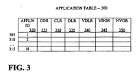
- FIG. 3 illustrates an exemplary application table 300 that stores information on each application installed on the single-chip data processing circuit 100, including the memory demands of each installed application.
- the application table 300 indicates the volatile, non-volatile and program storage (OTPROM) memory requirements of each application.
- OTPROM program storage
- the application table 300 may be generated by the microprocessor 110 when operating in a secure kernel mode, as each application is installed. The kernel allocates the appropriate memory areas to each application program.
- the application table 300 maintains a plurality of records, such as records 305-315, each associated with a different application. For each application identifier in field 320, the application table 300 includes the base address of where the application program code is stored in memory, and the corresponding size of the application code space in fields 325 and 330, respectively. In addition, the application table 300 indicates the total size of the data space in field 335 (sum of both the volatile and non-volatile memory), with the size of the allocated volatile memory stored in field 340, the base address for the scratchpad memory (RAM) in field 345, and the base address for non-volatile storage (EEPROM) is recorded in field 350. As previously indicated, when an application becomes active, each of the corresponding memory range values from fields 325 through 350 are retrieved and loaded into the appropriate limit and offset registers 230-232, 240-242, respectively.
- each of the corresponding memory range values from fields 325 through 350 are retrieved and loaded into the appropriate limit and offset registers 230-232, 240-242, respectively.
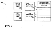
- FIG. 4 illustrates the memory partition control logic 400 for a homogeneous memory array 450.
- the memory partition control logic 400 contains registers associated with each portion of the homogeneous memory in order that the homogenous memory behaves like volatile, non-volatile and program storage (OTPROM) memory technologies, as desired.
- OTPROM program storage
- An application would normally be allocated different memory areas for code and data, and the data area can be further divided into a volatile portion, for scratchpad operations, and non-volatile storage areas.
- FERAM is inherently a non-volatile array. In other words, FERAM can be changed many times and holds the last written value, even when powered down, in a manner similar to EEPROM. Thus, it is unnecessary to force EEPROM-behavior onto the FERAM to achieve a non-volatile array.
- erase circuitry 410, 430 is added, for example, by writing 0's to each address, or using a block erase feature built into the array that writes 0's to many addresses in parallel.
- the erase circuitry 410, 430 records the upper and lower limits of the memory range that should behave like a volatile array.
- a write inhibit has to be forced onto the memory array using lock-write circuitry 420, 440.
- the lock-write circuitry 420, 440 records the upper and lower limits of the memory range that should behave like program storage (OTPROM) memory.
- the erase mechanism Before an application is started (or after or both), the erase mechanism is enabled, ensuring that an application when started can see no residual values left over by a previous application or the kernel, that may have used the designated block. Similarly, the same simple mechanism can be used to enforce a write-lock on the area designated as the code space for the application to prevent the application from modifying its code to cause potential unknown conditions and hence revealing secure aspects of the device.
- the application RAM area is defined by parameters loaded into erase circuitry 430. Typically, the value loaded into the erase circuitry 430 would be the physical address location within the FERAM memory array and the size of the allocated memory.
- the block erase logic 410 when activated, is constrained by the erase circuitry 430 to erase the predefined area. The same principle is used to obtain OTP characteristics.
- OTP partitioning is defined by the lock-write circuitry 440, which allocates an area of the same memory array once parameters are loaded.
- the lock write logic 420 removes the write capability for the area defined in the lock-write circuitry 440 giving the area the same characteristics as OTP memory.
Landscapes
- Engineering & Computer Science (AREA)
- Theoretical Computer Science (AREA)
- Physics & Mathematics (AREA)
- General Engineering & Computer Science (AREA)
- General Physics & Mathematics (AREA)
- Computer Security & Cryptography (AREA)
- Storage Device Security (AREA)
- Semiconductor Memories (AREA)
- Non-Volatile Memory (AREA)
- Controls And Circuits For Display Device (AREA)
Claims (18)
- Einchip-Datenverarbeitungsschaltung (100), umfassend:einen Prozessor (110) zum Ausführen einer Vielzahl von Anwendungen;eine homogene Speichereinheit (120, 130); undeine Speichermanagementeinheit (200) zum (i) Partionieren der homogenen Speichereinheit (120, 130) für jede aus der Vielzahl von Anwendungen, um Speichereigenschaften zu erzielen, die einer Vielzahl von Speichertechnologien zugeordnet sind, welche eine Technologie für flüchtige Speicher mit einschließen, (ii) Ansetzen für jede der Anwendungen einen Bereich für eine zugeordnete heterogene Speicherart, die jeder der Partitionen entspricht, und (iii) Auferlegen von Speichereigenschaften für eine heterogene Speicherart, die jeder der Partitionen für jede der Anwendungen entspricht.
- Einchip-Datenverarbeitungsschaltung nach Anspruch 1, wobei die Speichertechnologien eine ROM-Technologie mit begrenzter Programmierfähigkeit umfassen.
- Einchip-Datenverarbeitungsschaltung nach Anspruch 1, wobei die Speichertechnologien eine Technologie für nichtflüchtige Speicher umfassen.
- Einchip-Datenverarbeitungsschaltung nach Anspruch 1, wobei die Speichermanagementeinheit (200) eine Blocklöschlogik (410) umfasst, um Eigenschaften eines flüchtigen Speichers zu erzielen.
- Einchip-Datenverarbeitungsschaltung nach Anspruch 1, wobei die Speichermanagementeinheit eine Schreibsperrlogik (420) umfasst, um Eigenschaften eines Speichers mit begrenzter Programmierfähigkeit zu erzielen.
- Einchip-Datenverarbeitungsschaltung nach Anspruch 1, wobei die Speichermanagementeinheit (200) darüber hinaus ein Register umfasst, um eine Basisspeicheradresse zu speichern, die einem Ort entspricht, an dem ein nichtflüchtiger Speicherbereich beginnt.
- Einchip-Datenverarbeitungsschaltung nach Anspruch 1, wobei die Speichermanagementeinheit (200) darüber hinaus ein Register (230-232, 240-242) umfasst, um eine Speicheradresse zu speichern, die einem Ort entspricht, an dem ein nichtflüchtiger Speicherbereich endet.
- Einchip-Datenverarbeitungsschaltung nach Anspruch 1, wobei die Speichermanagementeinheit (200) darüber hinaus ein Register (230-232, 240-242) umfasst, um eine Basisspeicheradresse zu speichern, die einem Ort entspricht, an dem ein flüchtiger Speicherbereich beginnt.
- Einchip-Datenverarbeitungsschaltung nach Anspruch 1, wobei die Speichermanagementeinheit (200) darüber hinaus ein Register (230-232, 240-242) umfasst, um eine Speicheradresse zu speichern, die einem Ort entspricht, an dem ein flüchtiger Speicherbereich endet.
- Verfahren zum Partionieren einer homogenen Speichereinheit (120, 130), um für verschiedene Bereiche der Speichereinheit (120, 130) für eine Vielzahl von Anwendungen Eigenschaften eines heterogenen Speichers zu erzielen, die Schritte umfassend:Partionieren der homogenen Speichereinheit (120, 130), um Speichereigenschaften zu erzielen, die einer Vielzahl von Speichertechnologien zugeordnet sind, welche eine Technologie für flüchtige Speicher mit einschließen;Ansetzen für jede der Anwendungen einen Bereich für eine zugeordnete heterogene Speicherart, die jeder der Partitionen entspricht; undAuferlegen von Speichereigenschaften für eine heterogene Speicherart entsprechend jeder der Partitionen für jede der Anwendungen.
- Verfahren nach Anspruch 10, wobei die Speichertechnologien eine ROM-Technologie mit begrenzter Programmierfähigkeit umfassen.
- Verfahren nach Anspruch 10, wobei die Speichertechnologien eine Technologie für nichtflüchtige Speicher umfassen.
- Verfahren nach Anspruch 10, darüber hinaus den Schritt des Löschens einer Partition der homogenen Speichereinheit (120, 130) umfassend, um Eigenschaften eines flüchtigen Speichers zu erzielen.
- Verfahren nach Anspruch 10, darüber hinaus den Schritt umfassend, Schreibvorgänge in einer Partition zu verhindern, um Eigenschaften eines Speichers mit begrenzter Programmierfähigkeit zu erzielen.
- Verfahren nach Anspruch 10, darüber hinaus den Schritt umfassend, eine Basisspeicheradresse zu speichern, die einem Ort entspricht, an dem ein nichtflüchtiger Speicherbereich beginnt.
- Verfahren nach Anspruch 10, darüber hinaus den Schritt umfassend, eine Speicheradresse zu speichern, die einem Ort entspricht, an dem ein nichtflüchtiger Speicherbereich endet.
- Verfahren nach Anspruch 10, darüber hinaus den Schritt umfassend, eine Basisspeicheradresse zu speichern, die einem Ort entspricht, an dem ein flüchtiger Speicherbereich beginnt.
- Verfahren nach Anspruch 10, darüber hinaus den Schritt umfassend, eine Speicheradresse zu speichern, die einem Ort entspricht, an dem ein flüchtiger Speicherbereich endet.
Applications Claiming Priority (3)
| Application Number | Priority Date | Filing Date | Title |
|---|---|---|---|
| US09/420,318 US6292874B1 (en) | 1999-10-19 | 1999-10-19 | Memory management method and apparatus for partitioning homogeneous memory and restricting access of installed applications to predetermined memory ranges |
| US420318 | 1999-10-19 | ||
| PCT/US2000/041243 WO2001029672A1 (en) | 1999-10-19 | 2000-10-18 | Partitioned memory device having characteristics of different memory technologies |
Publications (3)
| Publication Number | Publication Date |
|---|---|
| EP1242891A1 EP1242891A1 (de) | 2002-09-25 |
| EP1242891A4 EP1242891A4 (de) | 2008-08-13 |
| EP1242891B1 true EP1242891B1 (de) | 2010-08-04 |
Family
ID=23665978
Family Applications (1)
| Application Number | Title | Priority Date | Filing Date |
|---|---|---|---|
| EP00984535A Expired - Lifetime EP1242891B1 (de) | 1999-10-19 | 2000-10-18 | Partitionierte speichervorrichtung mit merkmalen unterschiedlicher speichertechnologien |
Country Status (11)
| Country | Link |
|---|---|
| US (1) | US6292874B1 (de) |
| EP (1) | EP1242891B1 (de) |
| JP (1) | JP2003523554A (de) |
| KR (1) | KR100734340B1 (de) |
| AT (1) | ATE476706T1 (de) |
| AU (1) | AU771129B2 (de) |
| CA (1) | CA2387807A1 (de) |
| DE (1) | DE60044783D1 (de) |
| IL (1) | IL149157A0 (de) |
| NZ (1) | NZ518400A (de) |
| WO (1) | WO2001029672A1 (de) |
Families Citing this family (198)
| Publication number | Priority date | Publication date | Assignee | Title |
|---|---|---|---|---|
| ES2153455T3 (es) | 1995-08-04 | 2001-03-01 | Belle Gate Invest B V | Sistema de intercambio de datos que incluye unidades portatiles de procesamiento de datos. |
| US6385645B1 (en) * | 1995-08-04 | 2002-05-07 | Belle Gate Investments B.V. | Data exchange system comprising portable data processing units |
| US6295640B1 (en) * | 1998-05-08 | 2001-09-25 | Apple Computer, Inc. | Method and apparatus for distinguishing reference values from non-reference values in a runtime environment |
| US6996213B1 (en) | 1998-09-29 | 2006-02-07 | Sun Microsystems, Inc. | Superposition of data over voice |
| US6633984B2 (en) | 1999-01-22 | 2003-10-14 | Sun Microsystems, Inc. | Techniques for permitting access across a context barrier on a small footprint device using an entry point object |
| US6823520B1 (en) * | 1999-01-22 | 2004-11-23 | Sun Microsystems, Inc. | Techniques for implementing security on a small footprint device using a context barrier |
| US6907608B1 (en) * | 1999-01-22 | 2005-06-14 | Sun Microsystems, Inc. | Techniques for permitting access across a context barrier in a small footprint device using global data structures |
| US6922835B1 (en) | 1999-01-22 | 2005-07-26 | Sun Microsystems, Inc. | Techniques for permitting access across a context barrier on a small footprint device using run time environment privileges |
| US7093122B1 (en) | 1999-01-22 | 2006-08-15 | Sun Microsystems, Inc. | Techniques for permitting access across a context barrier in a small footprint device using shared object interfaces |
| ATE475139T1 (de) | 1999-06-10 | 2010-08-15 | Belle Gate Invest B V | Vorrichtung zum speichern unterschiedlicher versionen von datensätzen in getrennten datenbereichen und verfahren zur aktualisierung eines datensatzes in einem speicher |
| US6772416B1 (en) * | 1999-11-19 | 2004-08-03 | General Dynamics Decision Systems, Inc. | Separation kernel with memory allocation, remote procedure call and exception handling mechanisms |
| AU1586500A (en) | 1999-12-06 | 2001-06-12 | Sun Microsystems, Inc. | Computer arrangement using non-refreshed dram |
| US7080261B1 (en) | 1999-12-07 | 2006-07-18 | Sun Microsystems, Inc. | Computer-readable medium with microprocessor to control reading and computer arranged to communicate with such a medium |
| US6883716B1 (en) | 1999-12-07 | 2005-04-26 | Sun Microsystems, Inc. | Secure photo carrying identification device, as well as means and method for authenticating such an identification device |
| US6754815B1 (en) | 2000-03-31 | 2004-06-22 | Intel Corporation | Method and system for scrubbing an isolated area of memory after reset of a processor operating in isolated execution mode if a cleanup flag is set |
| US6957332B1 (en) | 2000-03-31 | 2005-10-18 | Intel Corporation | Managing a secure platform using a hierarchical executive architecture in isolated execution mode |
| US7082615B1 (en) * | 2000-03-31 | 2006-07-25 | Intel Corporation | Protecting software environment in isolated execution |
| US6990579B1 (en) | 2000-03-31 | 2006-01-24 | Intel Corporation | Platform and method for remote attestation of a platform |
| US6795905B1 (en) | 2000-03-31 | 2004-09-21 | Intel Corporation | Controlling accesses to isolated memory using a memory controller for isolated execution |
| US7013484B1 (en) * | 2000-03-31 | 2006-03-14 | Intel Corporation | Managing a secure environment using a chipset in isolated execution mode |
| US6760441B1 (en) | 2000-03-31 | 2004-07-06 | Intel Corporation | Generating a key hieararchy for use in an isolated execution environment |
| US7111176B1 (en) * | 2000-03-31 | 2006-09-19 | Intel Corporation | Generating isolated bus cycles for isolated execution |
| US6633963B1 (en) * | 2000-03-31 | 2003-10-14 | Intel Corporation | Controlling access to multiple memory zones in an isolated execution environment |
| US6996710B1 (en) | 2000-03-31 | 2006-02-07 | Intel Corporation | Platform and method for issuing and certifying a hardware-protected attestation key |
| US7013481B1 (en) | 2000-03-31 | 2006-03-14 | Intel Corporation | Attestation key memory device and bus |
| US6769058B1 (en) | 2000-03-31 | 2004-07-27 | Intel Corporation | Resetting a processor in an isolated execution environment |
| US6934817B2 (en) | 2000-03-31 | 2005-08-23 | Intel Corporation | Controlling access to multiple memory zones in an isolated execution environment |
| US7089418B1 (en) | 2000-03-31 | 2006-08-08 | Intel Corporation | Managing accesses in a processor for isolated execution |
| US7073071B1 (en) | 2000-03-31 | 2006-07-04 | Intel Corporation | Platform and method for generating and utilizing a protected audit log |
| US6678825B1 (en) | 2000-03-31 | 2004-01-13 | Intel Corporation | Controlling access to multiple isolated memories in an isolated execution environment |
| US7356817B1 (en) | 2000-03-31 | 2008-04-08 | Intel Corporation | Real-time scheduling of virtual machines |
| US7194634B2 (en) * | 2000-03-31 | 2007-03-20 | Intel Corporation | Attestation key memory device and bus |
| US7269631B2 (en) * | 2000-06-02 | 2007-09-11 | Hewlett-Packard Development Company, L.P. | Architecture for parallel distributed table driven I/O mapping |
| US6976162B1 (en) | 2000-06-28 | 2005-12-13 | Intel Corporation | Platform and method for establishing provable identities while maintaining privacy |
| DE10033612B4 (de) * | 2000-07-11 | 2004-05-13 | Siemens Ag | Verfahren zur Steuerung des Zugriffs auf eine Speichereinrichtung |
| DE60037342T2 (de) | 2000-07-20 | 2008-11-27 | Belle Gate Investment B.V. | Verfahren und system für kommunizierende geräte, und vorrichtungen dafür, mit geschützter datenübertragung |
| US7389427B1 (en) | 2000-09-28 | 2008-06-17 | Intel Corporation | Mechanism to secure computer output from software attack using isolated execution |
| US7793111B1 (en) | 2000-09-28 | 2010-09-07 | Intel Corporation | Mechanism to handle events in a machine with isolated execution |
| FR2816090B1 (fr) * | 2000-10-26 | 2003-01-10 | Schlumberger Systems & Service | Dispositif de partage de fichiers dans un dispositif a circuit integre |
| US7215781B2 (en) | 2000-12-22 | 2007-05-08 | Intel Corporation | Creation and distribution of a secret value between two devices |
| US7035963B2 (en) | 2000-12-27 | 2006-04-25 | Intel Corporation | Method for resolving address space conflicts between a virtual machine monitor and a guest operating system |
| US6907600B2 (en) * | 2000-12-27 | 2005-06-14 | Intel Corporation | Virtual translation lookaside buffer |
| US7818808B1 (en) | 2000-12-27 | 2010-10-19 | Intel Corporation | Processor mode for limiting the operation of guest software running on a virtual machine supported by a virtual machine monitor |
| US7225441B2 (en) | 2000-12-27 | 2007-05-29 | Intel Corporation | Mechanism for providing power management through virtualization |
| US7117376B2 (en) | 2000-12-28 | 2006-10-03 | Intel Corporation | Platform and method of creating a secure boot that enforces proper user authentication and enforces hardware configurations |
| US6567897B2 (en) * | 2001-03-01 | 2003-05-20 | International Business Machines Corporation | Virtualized NVRAM access methods to provide NVRAM CHRP regions for logical partitions through hypervisor system calls |
| GB0106082D0 (en) | 2001-03-13 | 2001-05-02 | Mat & Separations Tech Int Ltd | Method and equipment for removing volatile compounds from air |
| US7096497B2 (en) | 2001-03-30 | 2006-08-22 | Intel Corporation | File checking using remote signing authority via a network |
| DE10127179A1 (de) * | 2001-06-05 | 2002-12-19 | Infineon Technologies Ag | Verfahren zur Verwaltung eines Speichers einer Chipkarte |
| WO2003003194A1 (en) | 2001-06-27 | 2003-01-09 | Sony Corporation | Integrated circuit device, information processing device, information recording device memory management method, mobile terminal device, semiconductor integrated circuit device, and communication method using mobile terminal device |
| US7191440B2 (en) * | 2001-08-15 | 2007-03-13 | Intel Corporation | Tracking operating system process and thread execution and virtual machine execution in hardware or in a virtual machine monitor |
| US7024555B2 (en) | 2001-11-01 | 2006-04-04 | Intel Corporation | Apparatus and method for unilaterally loading a secure operating system within a multiprocessor environment |
| JP2003162433A (ja) * | 2001-11-27 | 2003-06-06 | Fujitsu Ltd | メモリシステム |
| US20030101381A1 (en) * | 2001-11-29 | 2003-05-29 | Nikolay Mateev | System and method for virus checking software |
| US7051340B2 (en) * | 2001-11-29 | 2006-05-23 | Hewlett-Packard Development Company, L.P. | System and method for isolating applications from each other |
| US7103771B2 (en) | 2001-12-17 | 2006-09-05 | Intel Corporation | Connecting a virtual token to a physical token |
| DE10164422A1 (de) * | 2001-12-29 | 2003-07-17 | Philips Intellectual Property | Verfahren und Anordnung zum Beschreiben von NV-Memories in einer Controller-Architektur sowie ein entsprechendes Computerprogrammprodukt und ein entsprechendes computerlesbares Speichermedium |
| US7308576B2 (en) | 2001-12-31 | 2007-12-11 | Intel Corporation | Authenticated code module |
| DE10200288A1 (de) * | 2002-01-07 | 2003-07-17 | Scm Microsystems Gmbh | Eine Vorrichtung zur Ausführung von Anwendungen, die sichere Transaktionen und/oder Zugangskontrolle zu werthaltigen Inhalten und/oder Dienstleistungen umfassen, und Verfahren zum Schutz einer solchen Vorrichtung |
| US7480806B2 (en) | 2002-02-22 | 2009-01-20 | Intel Corporation | Multi-token seal and unseal |
| US7631196B2 (en) | 2002-02-25 | 2009-12-08 | Intel Corporation | Method and apparatus for loading a trustable operating system |
| US7181737B2 (en) * | 2002-03-18 | 2007-02-20 | Sun Microsystems, Inc. | Method and apparatus for deployment of high integrity software using static procedure return addresses |
| US6996802B2 (en) * | 2002-03-18 | 2006-02-07 | Sun Microsystems, Inc. | Method and apparatus for deployment of high integrity software using initialization order and calling order constraints |
| US6912633B2 (en) * | 2002-03-18 | 2005-06-28 | Sun Microsystems, Inc. | Enhanced memory management for portable devices |
| US7010783B2 (en) * | 2002-03-18 | 2006-03-07 | Sun Microsystems, Inc. | Method and apparatus for deployment of high integrity software using reduced dynamic memory allocation |
| US20030182653A1 (en) * | 2002-03-22 | 2003-09-25 | Giuseppe Desoli | Systems and methods for verifying correct execution of emulated code via dynamic state verification |
| US7069442B2 (en) | 2002-03-29 | 2006-06-27 | Intel Corporation | System and method for execution of a secured environment initialization instruction |
| US7028149B2 (en) | 2002-03-29 | 2006-04-11 | Intel Corporation | System and method for resetting a platform configuration register |
| US7058807B2 (en) | 2002-04-15 | 2006-06-06 | Intel Corporation | Validation of inclusion of a platform within a data center |
| US7076669B2 (en) | 2002-04-15 | 2006-07-11 | Intel Corporation | Method and apparatus for communicating securely with a token |
| US7127548B2 (en) | 2002-04-16 | 2006-10-24 | Intel Corporation | Control register access virtualization performance improvement in the virtual-machine architecture |
| KR100476892B1 (ko) * | 2002-04-29 | 2005-03-17 | 삼성전자주식회사 | 데이터의 부정조작을 방지하는 방법 및 그것을 이용한데이터 처리 시스템 |
| US7139890B2 (en) | 2002-04-30 | 2006-11-21 | Intel Corporation | Methods and arrangements to interface memory |
| GB0212315D0 (en) * | 2002-05-28 | 2002-07-10 | Symbian Ltd | Secure mobile wireless device with protected file systems |
| JP3513147B2 (ja) | 2002-05-29 | 2004-03-31 | 株式会社ハギワラシスコム | Usbストレージデバイス及びその制御装置 |
| KR100505106B1 (ko) * | 2002-05-29 | 2005-07-29 | 삼성전자주식회사 | 강화된 보안 기능을 갖춘 스마트 카드 |
| US6820177B2 (en) * | 2002-06-12 | 2004-11-16 | Intel Corporation | Protected configuration space in a protected environment |
| KR20030096659A (ko) | 2002-06-17 | 2003-12-31 | 삼성전자주식회사 | 이미지 센서의 화소 어레이 영역, 그 구조체 및 그 제조방법 |
| US7142674B2 (en) | 2002-06-18 | 2006-11-28 | Intel Corporation | Method of confirming a secure key exchange |
| US7392415B2 (en) | 2002-06-26 | 2008-06-24 | Intel Corporation | Sleep protection |
| US6996748B2 (en) | 2002-06-29 | 2006-02-07 | Intel Corporation | Handling faults associated with operation of guest software in the virtual-machine architecture |
| US7124327B2 (en) | 2002-06-29 | 2006-10-17 | Intel Corporation | Control over faults occurring during the operation of guest software in the virtual-machine architecture |
| US7296267B2 (en) | 2002-07-12 | 2007-11-13 | Intel Corporation | System and method for binding virtual machines to hardware contexts |
| US8010405B1 (en) | 2002-07-26 | 2011-08-30 | Visa Usa Inc. | Multi-application smart card device software solution for smart cardholder reward selection and redemption |
| US8015060B2 (en) | 2002-09-13 | 2011-09-06 | Visa Usa, Inc. | Method and system for managing limited use coupon and coupon prioritization |
| US9852437B2 (en) | 2002-09-13 | 2017-12-26 | Visa U.S.A. Inc. | Opt-in/opt-out in loyalty system |
| US8626577B2 (en) | 2002-09-13 | 2014-01-07 | Visa U.S.A | Network centric loyalty system |
| US7121456B2 (en) | 2002-09-13 | 2006-10-17 | Visa U.S.A. Inc. | Method and system for managing token image replacement |
| US7171539B2 (en) * | 2002-11-18 | 2007-01-30 | Arm Limited | Apparatus and method for controlling access to a memory |
| US7383587B2 (en) * | 2002-11-18 | 2008-06-03 | Arm Limited | Exception handling control in a secure processing system |
| GB2396713B (en) * | 2002-11-18 | 2005-09-14 | Advanced Risc Mach Ltd | Apparatus and method for controlling access to a memory unit |
| GB2411027B (en) | 2002-11-18 | 2006-03-15 | Advanced Risc Mach Ltd | Control of access to a memory by a device |
| GB2396034B (en) * | 2002-11-18 | 2006-03-08 | Advanced Risc Mach Ltd | Technique for accessing memory in a data processing apparatus |
| GB0226874D0 (en) * | 2002-11-18 | 2002-12-24 | Advanced Risc Mach Ltd | Switching between secure and non-secure processing modes |
| RU2005115094A (ru) | 2002-11-18 | 2006-01-20 | Арм Лимитед (Gb) | Отображение адресов виртуальной памяти на физические адреса в системе с наличием защищенного домена и незащищенного домена |
| US6920611B1 (en) | 2002-11-25 | 2005-07-19 | Visa U.S.A., Inc. | Method and system for implementing a loyalty merchant component |
| US7165181B2 (en) | 2002-11-27 | 2007-01-16 | Intel Corporation | System and method for establishing trust without revealing identity |
| US7073042B2 (en) * | 2002-12-12 | 2006-07-04 | Intel Corporation | Reclaiming existing fields in address translation data structures to extend control over memory accesses |
| US7318235B2 (en) | 2002-12-16 | 2008-01-08 | Intel Corporation | Attestation using both fixed token and portable token |
| US7318141B2 (en) | 2002-12-17 | 2008-01-08 | Intel Corporation | Methods and systems to control virtual machines |
| US7793286B2 (en) * | 2002-12-19 | 2010-09-07 | Intel Corporation | Methods and systems to manage machine state in virtual machine operations |
| US7900017B2 (en) | 2002-12-27 | 2011-03-01 | Intel Corporation | Mechanism for remapping post virtual machine memory pages |
| US20040250105A1 (en) * | 2003-04-22 | 2004-12-09 | Ingo Molnar | Method and apparatus for creating an execution shield |
| US7827077B2 (en) | 2003-05-02 | 2010-11-02 | Visa U.S.A. Inc. | Method and apparatus for management of electronic receipts on portable devices |
| US20040243783A1 (en) * | 2003-05-30 | 2004-12-02 | Zhimin Ding | Method and apparatus for multi-mode operation in a semiconductor circuit |
| US7415708B2 (en) | 2003-06-26 | 2008-08-19 | Intel Corporation | Virtual machine management using processor state information |
| AU2003244914A1 (en) * | 2003-07-04 | 2005-01-21 | Nokia Corporation | Key storage administration |
| JP4537022B2 (ja) | 2003-07-09 | 2010-09-01 | 株式会社日立製作所 | データ配置に制限を設けるデータ処理方法、記憶領域制御方法、および、データ処理システム。 |
| US8554610B1 (en) | 2003-08-29 | 2013-10-08 | Visa U.S.A. Inc. | Method and system for providing reward status |
| US7104446B2 (en) | 2003-09-03 | 2006-09-12 | Visa U.S.A., Inc. | Method, system and portable consumer device using wildcard values |
| TWM249049U (en) * | 2003-09-09 | 2004-11-01 | Chicony Electronics Co Ltd | Digital camera |
| US7051923B2 (en) | 2003-09-12 | 2006-05-30 | Visa U.S.A., Inc. | Method and system for providing interactive cardholder rewards image replacement |
| US7424709B2 (en) | 2003-09-15 | 2008-09-09 | Intel Corporation | Use of multiple virtual machine monitors to handle privileged events |
| US7287197B2 (en) | 2003-09-15 | 2007-10-23 | Intel Corporation | Vectoring an interrupt or exception upon resuming operation of a virtual machine |
| US7739521B2 (en) | 2003-09-18 | 2010-06-15 | Intel Corporation | Method of obscuring cryptographic computations |
| US7610611B2 (en) | 2003-09-19 | 2009-10-27 | Moran Douglas R | Prioritized address decoder |
| US20050071656A1 (en) * | 2003-09-25 | 2005-03-31 | Klein Dean A. | Secure processor-based system and method |
| US7681046B1 (en) | 2003-09-26 | 2010-03-16 | Andrew Morgan | System with secure cryptographic capabilities using a hardware specific digital secret |
| US7177967B2 (en) | 2003-09-30 | 2007-02-13 | Intel Corporation | Chipset support for managing hardware interrupts in a virtual machine system |
| US8005763B2 (en) | 2003-09-30 | 2011-08-23 | Visa U.S.A. Inc. | Method and system for providing a distributed adaptive rules based dynamic pricing system |
| US7237051B2 (en) | 2003-09-30 | 2007-06-26 | Intel Corporation | Mechanism to control hardware interrupt acknowledgement in a virtual machine system |
| US20050080934A1 (en) | 2003-09-30 | 2005-04-14 | Cota-Robles Erik C. | Invalidating translation lookaside buffer entries in a virtual machine (VM) system |
| US7366305B2 (en) | 2003-09-30 | 2008-04-29 | Intel Corporation | Platform and method for establishing trust without revealing identity |
| US8407083B2 (en) | 2003-09-30 | 2013-03-26 | Visa U.S.A., Inc. | Method and system for managing reward reversal after posting |
| US7149863B1 (en) * | 2003-10-08 | 2006-12-12 | Sun Microsystems, Inc. | System and method of descriptively specifying memory placement in a computer system |
| DE10347828A1 (de) * | 2003-10-10 | 2005-05-25 | Giesecke & Devrient Gmbh | Zugreifen auf Datenelemente in einem tragbaren Datenträger |
| EP1676204A2 (de) * | 2003-10-13 | 2006-07-05 | Koninklijke Philips Electronics N.V. | Speicherungszuteilung pro anwendung |
| US7653602B2 (en) | 2003-11-06 | 2010-01-26 | Visa U.S.A. Inc. | Centralized electronic commerce card transactions |
| US7636844B2 (en) | 2003-11-17 | 2009-12-22 | Intel Corporation | Method and system to provide a trusted channel within a computer system for a SIM device |
| US7694151B1 (en) * | 2003-11-20 | 2010-04-06 | Johnson Richard C | Architecture, system, and method for operating on encrypted and/or hidden information |
| US8156343B2 (en) | 2003-11-26 | 2012-04-10 | Intel Corporation | Accessing private data about the state of a data processing machine from storage that is publicly accessible |
| US8037314B2 (en) | 2003-12-22 | 2011-10-11 | Intel Corporation | Replacing blinded authentication authority |
| US7802085B2 (en) | 2004-02-18 | 2010-09-21 | Intel Corporation | Apparatus and method for distributing private keys to an entity with minimal secret, unique information |
| US7356735B2 (en) | 2004-03-30 | 2008-04-08 | Intel Corporation | Providing support for single stepping a virtual machine in a virtual machine environment |
| US7620949B2 (en) | 2004-03-31 | 2009-11-17 | Intel Corporation | Method and apparatus for facilitating recognition of an open event window during operation of guest software in a virtual machine environment |
| US8171252B2 (en) * | 2004-04-09 | 2012-05-01 | Proton World International N.V. | Sharing of non-divisible files |
| US7490070B2 (en) | 2004-06-10 | 2009-02-10 | Intel Corporation | Apparatus and method for proving the denial of a direct proof signature |
| US7305592B2 (en) | 2004-06-30 | 2007-12-04 | Intel Corporation | Support for nested fault in a virtual machine environment |
| US7840962B2 (en) | 2004-09-30 | 2010-11-23 | Intel Corporation | System and method for controlling switching between VMM and VM using enabling value of VMM timer indicator and VMM timer value having a specified time |
| US8146078B2 (en) | 2004-10-29 | 2012-03-27 | Intel Corporation | Timer offsetting mechanism in a virtual machine environment |
| JP4750719B2 (ja) * | 2004-11-26 | 2011-08-17 | パナソニック株式会社 | プロセッサ、セキュア処理システム |
| US8924728B2 (en) | 2004-11-30 | 2014-12-30 | Intel Corporation | Apparatus and method for establishing a secure session with a device without exposing privacy-sensitive information |
| US8533777B2 (en) | 2004-12-29 | 2013-09-10 | Intel Corporation | Mechanism to determine trust of out-of-band management agents |
| DE102005000796A1 (de) * | 2005-01-05 | 2006-07-13 | Giesecke & Devrient Gmbh | Tragbarer Datenträger mit Wasserzeichen-Funktionalität |
| US7395405B2 (en) | 2005-01-28 | 2008-07-01 | Intel Corporation | Method and apparatus for supporting address translation in a virtual machine environment |
| KR100704037B1 (ko) * | 2005-04-15 | 2007-04-04 | 삼성전자주식회사 | 이종의 비휘발성 메모리를 가지는 데이터 저장장치와 그의구동 방법 |
| US7406711B2 (en) * | 2005-09-02 | 2008-07-29 | Motorola, Inc. | Method and apparatus for enforcing independence of processors on a single IC |
| US7809957B2 (en) | 2005-09-29 | 2010-10-05 | Intel Corporation | Trusted platform module for generating sealed data |
| US9573067B2 (en) * | 2005-10-14 | 2017-02-21 | Microsoft Technology Licensing, Llc | Mass storage in gaming handhelds |
| US7496727B1 (en) | 2005-12-06 | 2009-02-24 | Transmeta Corporation | Secure memory access system and method |
| US7845005B2 (en) * | 2006-02-07 | 2010-11-30 | International Business Machines Corporation | Method for preventing malicious software installation on an internet-connected computer |
| US8014530B2 (en) | 2006-03-22 | 2011-09-06 | Intel Corporation | Method and apparatus for authenticated, recoverable key distribution with no database secrets |
| US7650479B2 (en) * | 2006-09-20 | 2010-01-19 | Arm Limited | Maintaining cache coherency for secure and non-secure data access requests |
| US20080077749A1 (en) * | 2006-09-22 | 2008-03-27 | Daniel Scott Cohen | Access control of memory space in microprocessor systems |
| FR2908916B1 (fr) * | 2006-11-17 | 2009-04-17 | Thales Sa | Systeme de traitement d'objets graphiques comportant un gestionnaire graphique securise |
| SG146551A1 (en) * | 2007-03-29 | 2008-10-30 | Toshiba Kk | Portable electronic device and control method of portable electronic device |
| DE602007012519D1 (de) | 2007-04-05 | 2011-03-31 | St Microelectronics Res & Dev | Integrierte Schaltung mit beschränktem Datenzugang |
| US20080270652A1 (en) * | 2007-04-30 | 2008-10-30 | Jeffrey Kevin Jeansonne | System and method of tamper-resistant control |
| US8213612B2 (en) * | 2007-12-07 | 2012-07-03 | Inside Contactless S.A. | Secure software download |
| FR2929729A1 (fr) * | 2008-04-03 | 2009-10-09 | Alveol Technology Sarl | Dispositif de gestion de la memoire d'un environnement informatique |
| WO2010031976A1 (fr) * | 2008-09-22 | 2010-03-25 | France Telecom | Procède d'allocation de mémoire et procède de gestion de données associe a une application enregistrée dans un module de sécurité associe a un terminal, module de sécurité et terminal associes |
| KR101481562B1 (ko) * | 2008-09-22 | 2015-01-13 | 엘지전자 주식회사 | 디지털 방송 수신 장치 및 그의 동작 메모리 설정 방법 |
| KR101573047B1 (ko) | 2009-01-23 | 2015-12-02 | 삼성전자주식회사 | 복합 메모리 장치 및 이를 이용한 i/o 처리 방법 |
| RU2422883C1 (ru) * | 2009-12-09 | 2011-06-27 | Корпорация "САМСУНГ ЭЛЕКТРОНИКС Ко., Лтд." | Система и способ размещения статических объектов данных в неоднородной оперативной памяти |
| US7992781B2 (en) | 2009-12-16 | 2011-08-09 | Visa International Service Association | Merchant alerts incorporating receipt data |
| US8429048B2 (en) | 2009-12-28 | 2013-04-23 | Visa International Service Association | System and method for processing payment transaction receipts |
| KR101119434B1 (ko) * | 2010-05-26 | 2012-03-16 | 주식회사 켐트로닉스 | 하나의 메모리를 공유하는 마이크로 콘트롤러 유닛, 이에 포함되는 메모리 관리 방법 및 그 방법을 실행하는 프로그램이 기록된 기록 매체 |
| US8539245B2 (en) * | 2010-08-06 | 2013-09-17 | Intel Corporation | Apparatus and method for accessing a secure partition in non-volatile storage by a host system enabled after the system exits a first instance of a secure mode |
| US9378142B2 (en) | 2011-09-30 | 2016-06-28 | Intel Corporation | Apparatus and method for implementing a multi-level memory hierarchy having different operating modes |
| EP2761468B1 (de) * | 2011-09-30 | 2019-12-11 | Intel Corporation | Plattformspeicherhierarchie mit einem nichtflüchtigen ram-speicher mit konfigurierbaren partitionen |
| US9378133B2 (en) | 2011-09-30 | 2016-06-28 | Intel Corporation | Autonomous initialization of non-volatile random access memory in a computer system |
| EP3364304B1 (de) | 2011-09-30 | 2022-06-15 | INTEL Corporation | Speicherkanal zur unterstützung von nah- und fernspeicherzugriffen |
| EP2761469B1 (de) * | 2011-09-30 | 2019-11-13 | Intel Corporation | Nichtflüchtiger direktzugriffsspeicher (nvram) als ersatz für herkömmlichen massenspeicher |
| EP2761476B1 (de) | 2011-09-30 | 2017-10-25 | Intel Corporation | Vorrichtung, verfahren und system zur bios-speicherung in einer nichtflüchtige ram-speicherzelle |
| US8667270B2 (en) | 2012-02-10 | 2014-03-04 | Samsung Electronics Co., Ltd. | Securely upgrading or downgrading platform components |
| US9286235B2 (en) * | 2012-06-29 | 2016-03-15 | Intel Corporation | Virtual memory address range register |
| US9075751B2 (en) * | 2012-08-09 | 2015-07-07 | Intel Corporation | Secure data protection with improved read-only memory locking during system pre-boot |
| KR102002900B1 (ko) | 2013-01-07 | 2019-07-23 | 삼성전자 주식회사 | 메모리 관리 유닛을 포함하는 시스템 온 칩 및 그 메모리 주소 변환 방법 |
| US9224452B2 (en) | 2013-01-17 | 2015-12-29 | Qualcomm Incorporated | Heterogeneous memory systems, and related methods and computer-readable media for supporting heterogeneous memory access requests in processor-based systems |
| KR102088403B1 (ko) | 2013-08-08 | 2020-03-13 | 삼성전자 주식회사 | 저장장치, 이를 포함하는 컴퓨터 시스템 및 이의 동작 방법 |
| US20160048353A1 (en) * | 2014-08-13 | 2016-02-18 | Kabushiki Kaisha Toshiba | Memory system and method of controlling memory system |
| DE102015200801A1 (de) * | 2015-01-20 | 2016-07-21 | Continental Teves Ag & Co. Ohg | Elektronische Steuerungsvorrichtung |
| US9405515B1 (en) * | 2015-02-04 | 2016-08-02 | Rockwell Collins, Inc. | Computing systems utilizing controlled dynamic libraries and isolated execution spaces |
| US9904586B2 (en) * | 2015-10-28 | 2018-02-27 | Intel Corporation | Interfacing with block-based storage in a processor |
| US9747041B2 (en) | 2015-12-23 | 2017-08-29 | Intel Corporation | Apparatus and method for a non-power-of-2 size cache in a first level memory device to cache data present in a second level memory device |
| US10007606B2 (en) | 2016-03-30 | 2018-06-26 | Intel Corporation | Implementation of reserved cache slots in computing system having inclusive/non inclusive tracking and two level system memory |
| US10185619B2 (en) | 2016-03-31 | 2019-01-22 | Intel Corporation | Handling of error prone cache line slots of memory side cache of multi-level system memory |
| US10120806B2 (en) | 2016-06-27 | 2018-11-06 | Intel Corporation | Multi-level system memory with near memory scrubbing based on predicted far memory idle time |
| CN107665175A (zh) * | 2016-07-27 | 2018-02-06 | 展讯通信(上海)有限公司 | 存储器分区隔离的方法、装置及电子设备 |
| US10915453B2 (en) | 2016-12-29 | 2021-02-09 | Intel Corporation | Multi level system memory having different caching structures and memory controller that supports concurrent look-up into the different caching structures |
| US10445261B2 (en) | 2016-12-30 | 2019-10-15 | Intel Corporation | System memory having point-to-point link that transports compressed traffic |
| US10304814B2 (en) | 2017-06-30 | 2019-05-28 | Intel Corporation | I/O layout footprint for multiple 1LM/2LM configurations |
| US11188467B2 (en) | 2017-09-28 | 2021-11-30 | Intel Corporation | Multi-level system memory with near memory capable of storing compressed cache lines |
| US10860244B2 (en) | 2017-12-26 | 2020-12-08 | Intel Corporation | Method and apparatus for multi-level memory early page demotion |
| US20190258812A1 (en) * | 2018-02-20 | 2019-08-22 | Sensata Technologies, Inc. | Memory security for automotive functional safety compliance with independent downstream processes |
| KR102745459B1 (ko) | 2018-12-18 | 2024-12-20 | 에스케이하이닉스 주식회사 | 스마트 카 시스템 |
| US11055228B2 (en) | 2019-01-31 | 2021-07-06 | Intel Corporation | Caching bypass mechanism for a multi-level memory |
| KR102881581B1 (ko) | 2021-07-14 | 2025-11-07 | 삼성전자주식회사 | 반도체 소자 및 그의 제조 방법 |
Family Cites Families (10)
| Publication number | Priority date | Publication date | Assignee | Title |
|---|---|---|---|---|
| JP2514954B2 (ja) * | 1987-03-13 | 1996-07-10 | 三菱電機株式会社 | Icカ−ド |
| JP2682700B2 (ja) * | 1989-05-09 | 1997-11-26 | 三菱電機株式会社 | Icカード |
| JPH03276337A (ja) * | 1990-03-27 | 1991-12-06 | Toshiba Corp | マイクロコントローラ |
| JP3178881B2 (ja) * | 1992-03-06 | 2001-06-25 | 株式会社東芝 | 携帯可能電子装置 |
| JPH05120891A (ja) * | 1992-04-24 | 1993-05-18 | Hitachi Ltd | 半導体記憶装置 |
| JPH06274397A (ja) * | 1993-03-24 | 1994-09-30 | Toshiba Corp | ファイル管理方式 |
| JPH07114497A (ja) * | 1993-10-14 | 1995-05-02 | Hitachi Ltd | 半導体集積回路装置 |
| DE19536169A1 (de) * | 1995-09-29 | 1997-04-03 | Ibm | Multifunktionale Chipkarte |
| US5818771A (en) * | 1996-09-30 | 1998-10-06 | Hitachi, Ltd. | Semiconductor memory device |
| US5890199A (en) * | 1996-10-21 | 1999-03-30 | Ramtron International Corporation | Data processor incorporating a ferroelectric memory array selectably configurable as read/write and read only memory |
-
1999
- 1999-10-19 US US09/420,318 patent/US6292874B1/en not_active Expired - Lifetime
-
2000
- 2000-10-18 IL IL14915700A patent/IL149157A0/xx unknown
- 2000-10-18 CA CA002387807A patent/CA2387807A1/en not_active Abandoned
- 2000-10-18 JP JP2001532399A patent/JP2003523554A/ja active Pending
- 2000-10-18 EP EP00984535A patent/EP1242891B1/de not_active Expired - Lifetime
- 2000-10-18 WO PCT/US2000/041243 patent/WO2001029672A1/en not_active Ceased
- 2000-10-18 AT AT00984535T patent/ATE476706T1/de not_active IP Right Cessation
- 2000-10-18 DE DE60044783T patent/DE60044783D1/de not_active Expired - Lifetime
- 2000-10-18 KR KR1020027005035A patent/KR100734340B1/ko not_active Expired - Lifetime
- 2000-10-18 AU AU21137/01A patent/AU771129B2/en not_active Ceased
- 2000-10-18 NZ NZ518400A patent/NZ518400A/xx unknown
Also Published As
| Publication number | Publication date |
|---|---|
| KR100734340B1 (ko) | 2007-07-03 |
| WO2001029672A9 (en) | 2002-08-08 |
| AU771129B2 (en) | 2004-03-11 |
| ATE476706T1 (de) | 2010-08-15 |
| WO2001029672A1 (en) | 2001-04-26 |
| IL149157A0 (en) | 2002-11-10 |
| EP1242891A1 (de) | 2002-09-25 |
| DE60044783D1 (de) | 2010-09-16 |
| US6292874B1 (en) | 2001-09-18 |
| AU2113701A (en) | 2001-04-30 |
| KR20020039374A (ko) | 2002-05-25 |
| CA2387807A1 (en) | 2001-04-26 |
| NZ518400A (en) | 2003-01-31 |
| JP2003523554A (ja) | 2003-08-05 |
| EP1242891A4 (de) | 2008-08-13 |
Similar Documents
| Publication | Publication Date | Title |
|---|---|---|
| US6292874B1 (en) | Memory management method and apparatus for partitioning homogeneous memory and restricting access of installed applications to predetermined memory ranges | |
| KR102095614B1 (ko) | 메모리 보호 | |
| JP2727520B2 (ja) | メモリカード及びその作動方法 | |
| CN112602061B (zh) | 在计算机处理器中执行指令时的域交叉 | |
| US7975117B2 (en) | Enforcing isolation among plural operating systems | |
| KR20050113659A (ko) | 메모리 장치 | |
| US7260690B2 (en) | Microprocessor circuit for data carriers and method for organizing access to data stored in a memory | |
| CN112639732A (zh) | 基于超管理器的存在的计算机处理器的动态配置 | |
| US20100023780A1 (en) | Flash device security method utilizing a check register | |
| US20030105968A1 (en) | System and method for migration of a version of a bootable program | |
| CN110268392A (zh) | 安全架构和方法 | |
| GB2356469A (en) | Portable data carrier memory management system and method | |
| US20230161486A1 (en) | Method for managing a memory in a system-on-a-chip | |
| US20240370382A1 (en) | System-on-chip having a memory controller and corresponding memory control method | |
| US12039090B2 (en) | Integrated circuit with asymmetric access privileges |
Legal Events
| Date | Code | Title | Description |
|---|---|---|---|
| PUAI | Public reference made under article 153(3) epc to a published international application that has entered the european phase |
Free format text: ORIGINAL CODE: 0009012 |
|
| 17P | Request for examination filed |
Effective date: 20020419 |
|
| AK | Designated contracting states |
Kind code of ref document: A1 Designated state(s): AT BE CH CY DE DK ES FI FR GB GR IE IT LI LU MC NL PT SE |
|
| AX | Request for extension of the european patent |
Free format text: AL;LT;LV;MK;RO;SI |
|
| A4 | Supplementary search report drawn up and despatched |
Effective date: 20080716 |
|
| RAP1 | Party data changed (applicant data changed or rights of an application transferred) |
Owner name: EMOSYN AMERICA, INC. |
|
| RAP1 | Party data changed (applicant data changed or rights of an application transferred) |
Owner name: SILICON STORAGE TECHNOLOGY, INC. |
|
| 17Q | First examination report despatched |
Effective date: 20090218 |
|
| GRAP | Despatch of communication of intention to grant a patent |
Free format text: ORIGINAL CODE: EPIDOSNIGR1 |
|
| GRAS | Grant fee paid |
Free format text: ORIGINAL CODE: EPIDOSNIGR3 |
|
| GRAA | (expected) grant |
Free format text: ORIGINAL CODE: 0009210 |
|
| AK | Designated contracting states |
Kind code of ref document: B1 Designated state(s): AT BE CH CY DE DK ES FI FR GB GR IE IT LI LU MC NL PT SE |
|
| REG | Reference to a national code |
Ref country code: GB Ref legal event code: FG4D |
|
| REG | Reference to a national code |
Ref country code: CH Ref legal event code: EP |
|
| REG | Reference to a national code |
Ref country code: IE Ref legal event code: FG4D |
|
| REF | Corresponds to: |
Ref document number: 60044783 Country of ref document: DE Date of ref document: 20100916 Kind code of ref document: P |
|
| REG | Reference to a national code |
Ref country code: NL Ref legal event code: VDEP Effective date: 20100804 |
|
| PG25 | Lapsed in a contracting state [announced via postgrant information from national office to epo] |
Ref country code: AT Free format text: LAPSE BECAUSE OF FAILURE TO SUBMIT A TRANSLATION OF THE DESCRIPTION OR TO PAY THE FEE WITHIN THE PRESCRIBED TIME-LIMIT Effective date: 20100804 Ref country code: NL Free format text: LAPSE BECAUSE OF FAILURE TO SUBMIT A TRANSLATION OF THE DESCRIPTION OR TO PAY THE FEE WITHIN THE PRESCRIBED TIME-LIMIT Effective date: 20100804 Ref country code: FI Free format text: LAPSE BECAUSE OF FAILURE TO SUBMIT A TRANSLATION OF THE DESCRIPTION OR TO PAY THE FEE WITHIN THE PRESCRIBED TIME-LIMIT Effective date: 20100804 |
|
| PG25 | Lapsed in a contracting state [announced via postgrant information from national office to epo] |
Ref country code: PT Free format text: LAPSE BECAUSE OF FAILURE TO SUBMIT A TRANSLATION OF THE DESCRIPTION OR TO PAY THE FEE WITHIN THE PRESCRIBED TIME-LIMIT Effective date: 20101206 Ref country code: CY Free format text: LAPSE BECAUSE OF FAILURE TO SUBMIT A TRANSLATION OF THE DESCRIPTION OR TO PAY THE FEE WITHIN THE PRESCRIBED TIME-LIMIT Effective date: 20100804 |
|
| PGFP | Annual fee paid to national office [announced via postgrant information from national office to epo] |
Ref country code: DE Payment date: 20101022 Year of fee payment: 11 |
|
| PG25 | Lapsed in a contracting state [announced via postgrant information from national office to epo] |
Ref country code: BE Free format text: LAPSE BECAUSE OF FAILURE TO SUBMIT A TRANSLATION OF THE DESCRIPTION OR TO PAY THE FEE WITHIN THE PRESCRIBED TIME-LIMIT Effective date: 20100804 Ref country code: GR Free format text: LAPSE BECAUSE OF FAILURE TO SUBMIT A TRANSLATION OF THE DESCRIPTION OR TO PAY THE FEE WITHIN THE PRESCRIBED TIME-LIMIT Effective date: 20101105 Ref country code: SE Free format text: LAPSE BECAUSE OF FAILURE TO SUBMIT A TRANSLATION OF THE DESCRIPTION OR TO PAY THE FEE WITHIN THE PRESCRIBED TIME-LIMIT Effective date: 20100804 |
|
| PG25 | Lapsed in a contracting state [announced via postgrant information from national office to epo] |
Ref country code: DK Free format text: LAPSE BECAUSE OF FAILURE TO SUBMIT A TRANSLATION OF THE DESCRIPTION OR TO PAY THE FEE WITHIN THE PRESCRIBED TIME-LIMIT Effective date: 20100804 |
|
| PG25 | Lapsed in a contracting state [announced via postgrant information from national office to epo] |
Ref country code: IT Free format text: LAPSE BECAUSE OF FAILURE TO SUBMIT A TRANSLATION OF THE DESCRIPTION OR TO PAY THE FEE WITHIN THE PRESCRIBED TIME-LIMIT Effective date: 20100804 Ref country code: MC Free format text: LAPSE BECAUSE OF NON-PAYMENT OF DUE FEES Effective date: 20101031 |
|
| REG | Reference to a national code |
Ref country code: CH Ref legal event code: PL |
|
| PLBE | No opposition filed within time limit |
Free format text: ORIGINAL CODE: 0009261 |
|
| STAA | Information on the status of an ep patent application or granted ep patent |
Free format text: STATUS: NO OPPOSITION FILED WITHIN TIME LIMIT |
|
| PG25 | Lapsed in a contracting state [announced via postgrant information from national office to epo] |
Ref country code: ES Free format text: LAPSE BECAUSE OF FAILURE TO SUBMIT A TRANSLATION OF THE DESCRIPTION OR TO PAY THE FEE WITHIN THE PRESCRIBED TIME-LIMIT Effective date: 20101115 |
|
| 26N | No opposition filed |
Effective date: 20110506 |
|
| GBPC | Gb: european patent ceased through non-payment of renewal fee |
Effective date: 20101104 |
|
| PG25 | Lapsed in a contracting state [announced via postgrant information from national office to epo] |
Ref country code: CH Free format text: LAPSE BECAUSE OF NON-PAYMENT OF DUE FEES Effective date: 20101031 Ref country code: LI Free format text: LAPSE BECAUSE OF NON-PAYMENT OF DUE FEES Effective date: 20101031 |
|
| REG | Reference to a national code |
Ref country code: DE Ref legal event code: R097 Ref document number: 60044783 Country of ref document: DE Effective date: 20110506 |
|
| PG25 | Lapsed in a contracting state [announced via postgrant information from national office to epo] |
Ref country code: IE Free format text: LAPSE BECAUSE OF NON-PAYMENT OF DUE FEES Effective date: 20101018 |
|
| PG25 | Lapsed in a contracting state [announced via postgrant information from national office to epo] |
Ref country code: GB Free format text: LAPSE BECAUSE OF NON-PAYMENT OF DUE FEES Effective date: 20101104 |
|
| PGFP | Annual fee paid to national office [announced via postgrant information from national office to epo] |
Ref country code: FR Payment date: 20111103 Year of fee payment: 12 |
|
| PG25 | Lapsed in a contracting state [announced via postgrant information from national office to epo] |
Ref country code: LU Free format text: LAPSE BECAUSE OF NON-PAYMENT OF DUE FEES Effective date: 20101018 |
|
| REG | Reference to a national code |
Ref country code: FR Ref legal event code: ST Effective date: 20130628 |
|
| PG25 | Lapsed in a contracting state [announced via postgrant information from national office to epo] |
Ref country code: DE Free format text: LAPSE BECAUSE OF NON-PAYMENT OF DUE FEES Effective date: 20130501 |
|
| REG | Reference to a national code |
Ref country code: DE Ref legal event code: R119 Ref document number: 60044783 Country of ref document: DE Effective date: 20130501 |
|
| PG25 | Lapsed in a contracting state [announced via postgrant information from national office to epo] |
Ref country code: FR Free format text: LAPSE BECAUSE OF NON-PAYMENT OF DUE FEES Effective date: 20121031 |