EP1239627A2 - Clock/Data recovery circuit - Google Patents
Clock/Data recovery circuit Download PDFInfo
- Publication number
- EP1239627A2 EP1239627A2 EP02251533A EP02251533A EP1239627A2 EP 1239627 A2 EP1239627 A2 EP 1239627A2 EP 02251533 A EP02251533 A EP 02251533A EP 02251533 A EP02251533 A EP 02251533A EP 1239627 A2 EP1239627 A2 EP 1239627A2
- Authority
- EP
- European Patent Office
- Prior art keywords
- signal
- clock
- clock signal
- output
- circuit
- Prior art date
- Legal status (The legal status is an assumption and is not a legal conclusion. Google has not performed a legal analysis and makes no representation as to the accuracy of the status listed.)
- Granted
Links
Images

















Classifications
-
- H—ELECTRICITY
- H04—ELECTRIC COMMUNICATION TECHNIQUE
- H04L—TRANSMISSION OF DIGITAL INFORMATION, e.g. TELEGRAPHIC COMMUNICATION
- H04L7/00—Arrangements for synchronising receiver with transmitter
- H04L7/02—Speed or phase control by the received code signals, the signals containing no special synchronisation information
- H04L7/033—Speed or phase control by the received code signals, the signals containing no special synchronisation information using the transitions of the received signal to control the phase of the synchronising-signal-generating means, e.g. using a phase-locked loop
- H04L7/0337—Selecting between two or more discretely delayed clocks or selecting between two or more discretely delayed received code signals
-
- H—ELECTRICITY
- H03—ELECTRONIC CIRCUITRY
- H03L—AUTOMATIC CONTROL, STARTING, SYNCHRONISATION OR STABILISATION OF GENERATORS OF ELECTRONIC OSCILLATIONS OR PULSES
- H03L7/00—Automatic control of frequency or phase; Synchronisation
- H03L7/06—Automatic control of frequency or phase; Synchronisation using a reference signal applied to a frequency- or phase-locked loop
- H03L7/08—Details of the phase-locked loop
-
- H—ELECTRICITY
- H04—ELECTRIC COMMUNICATION TECHNIQUE
- H04J—MULTIPLEX COMMUNICATION
- H04J3/00—Time-division multiplex systems
- H04J3/02—Details
- H04J3/04—Distributors combined with modulators or demodulators
- H04J3/047—Distributors with transistors or integrated circuits
Definitions
- the clock/data recovery circuit is applied to a receiver part and the like of an optical front end circuit in a router or a cross-connect switch of point to point transmission, GbE/10GbE, Fibre Channel in an optical communication system.
- Fig.1 shows a configuration of a conventional clock/data recovery circuit.
- This configuration is a PLL configuration using the voltage control oscillator which outputs a clock signal of a frequency of 1/2 of bit rate of an input data signal (refer to: M.Wurzer,et.al.,"A 40-Gb/s Integrated Clock and Data Recovery Circuit in a 50-GHz Silicon Bipolar Technology,”IEEE J.Solid-State Circuits, VOL.34, NO.9, pp.1320-1324 Sep.1999).
- This clock/data recovery circuit includes a voltage control oscillator (VOC) 51 which outputs a clock signal CLK1 at a frequency of 1/2 of bit rate of an input data signal DIN, D-type ms-flip flop circuits (DFF) 52 and 53 (which write data at a rising edge), a 90-degree delay circuit 54 which delays phase of a signal by 90-degree, a D-type ms-flip flop circuit 55 which receives a clock signal CLK2 output from the 90-degree delay circuit 54, an EXOR circuit 56 which compares phases of signals D2 and D3 output from D-type ms-flip flop circuits 53 and 55, a lowpass filter (LPF) 57 which extracts DC voltage from the phase compared signal output from the EXOR circuit 56 and inputs the DC voltage to the voltage control oscillator 51 as a control voltage.
- D1 is an output signal of the D-type ms-flip flop circuit 52.
- Fig.2 shows a timing chart of the signals DIN, D2, CLK1, CLK2 of the clock/data recovery circuit.
- (a), (b), (c) indicate a lock status, a lead status of the clock signal CLK1 and a lag status of the clock signal CLK1 respectively.
- the rising/falling edge of the clock signal CLK1 becomes the same timing as a center between edges of the input data signal DIN
- the rising/falling edge of the clock signal CLK2 becomes the same timing as an edge of the input data signal DIN.
- the EXOR circuit 56 When there are data transitions (1 ⁇ 0, 0 ⁇ 1) in the input data signal DIN, the EXOR circuit 56 outputs an output signal according to lead/lag relationship of the phase of the input data signal DIN and the clock signal CLK1.
- the output signal of the EXOR circuit 56 is determined according to lead/lag status of the clock signal CLK1 with respect to the input data signal DIN. Then, a DC signal obtained by extracting DC voltage from the output signal by the lowpass filter 57 is input to the voltage control oscillator 51 as the feedback signal.
- a clock/data recovery circuit which can perform pull-in by using the voltage control oscillator having an oscillation frequency of a half of an oscillation frequency of a voltage control oscillator of a clock/data recovery circuit using PLL can be realized.
- Fig.2(a) represents a timing chart of the ideal lock status.
- the edge of the clock signals CLK1 and CLK2 of Fig.1 in an actual lock status repeats, as shown in Fig.3 (a), lead/lag movement with respect to the phase of the input data signal DIN around the pulse center t1 and the edge t2 of the input data signal DIN.
- the ratio of the number of cases that the output of the EXOR circuit 56 is 1 to the number of cases that the output of the EXOR circuit 56 is 0 is determined, so that the output voltage of the lowpass filter 57 which is fed back to the voltage control oscillator 51 can be determined.
- the ratio RLL of the lead/lag status number is determined by feeding a voltage proportionate to fd back to the voltage control oscillator 51, the phase difference (the magnitude of lead/lag) is not decided. That is, there may be a case in which RLL is the same and the phase magnitude of each lead/lag status is different (Fig.3 (b), (c)). Fig.3(b) shows a case when the magnitude of lead/lag is small and Fig.3(c) shows a case when the amount of lead/lag is large.
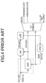
- FIG. 4 Another example of the conventional CDR (Clock and Data Recovery), as shown in Fig.4, is one using VCO having the same oscillation frequency as the input data bit rate.
- This CDR circuit extracts a clock signal CLK from the input data signal DATAIN, discriminates data signal.
- DEMUX demultiplexer
- the DEMUX outputs low speed parallel data signals demultiplexed of serial data signal output from CDR.
- the operation speed required for VCO becomes double and there is a problem in that speedup becomes difficult.
- An object of the present invention is to provide a clock/data recovery circuit realizing low jitter while a voltage control oscillator which oscillates at 1/K frequency of the bit rate of the input data signal is used.
- the object of the present invention is to provide a clock/data recovery circuit realizing a serial signal output function (clock and data) in addition to a parallel signal output function.
- a clock/data recovery circuit including:
- M K ⁇ L in which L is a natural number.
- the clock/data recovery circuit may includes:
- the demultiplexer may include:
- the demultiplexer may include:
- the demultiplexer may include:
- the demultiplexer may include:
- a clock/data recovery circuit including:
- M K ⁇ L in which L is a natural number.
- the clock/data recovery circuit may include:
- the first demultiplexer may include:
- the voltage control oscillator instead of providing the 90-degree delay circuit, the voltage control oscillator outputs a quadrature clock signal having the same frequency as the clock signal and being quadrature to the clock signal, the multiplier receives the clock signal and the quadrature clock signal and outputs a clock signal having the same frequency as bit rate of the input data signal.
- the clock/data recovery circuit may include:
- the voltage control oscillator may include 2k (k ⁇ 1) buffer circuits having the same delay time in which the delay time is controlled by a control voltage, the buffer circuits being connected in series, an inverted signal of output of 2kth buffer circuit is input to a first stage buffer circuit; and an input of the first stage buffer circuit is the clock signal and an output of kth stage buffer circuit is the quadrature clock signal.
- the K multiplier may include:
- a receiving apparatus including a clock/data recovery circuit, the clock/data recovery circuit including:
- the input data signal is converted into a data signal in which the phase corresponds with that of the output clock signal of the voltage control oscillator by performing demultiplexing/multiplexing operation.
- the phase comparison signal according to the phase difference can be output even when a voltage control oscillator of frequency of 1/2 of that of the conventional circuit is used, and the feedback voltage to the voltage control oscillator becomes a voltage according to phase difference.
- low jitter can be realized.
- a receiving apparatus including the clock/data recovery circuit can be provided.
- the receiving apparatus can be applied to an optical front end circuit receiver and the like in a router or in a cross connect part in SDH/SONET, point to point transmission, GbE/10GbE and Fiber Channel in an optical communication system.
- the low jitter, small size and low power consumption can be realized.
- lowering cost of an optical front end module can be realized and the cost of a communication system can be decreased.
- oscillation signal of voltage control oscillator which oscillates a clock signal of 1/K frequency of bit rate of the input data signal
- data signal the phase timing of which coincides with that of the oscillation signal of the voltage control oscillator is generated by performing demultiplexing and multiplexing for the input signal, the phase of this data signal is compared with the phase of the input data signal by the phase comparator.
- output signal phase of the voltage control oscillator is determined uniquely according to difference between a value two times of free-running frequency of the voltage control oscillator and the bit rate value of the input data signal in the lock status, and low jitter can be realized.
- the performance of the clock/data recovery circuit can be enhanced.
- Fig.5 shows a first embodiment of the present invention.
- 1 indicates a 90-degree delay circuit which delays phase of the input data signal DIN by 90-degree
- 2 indicates a voltage control oscillator (VCO) which oscillates at a frequency of 1/2 of the bit rate of the input data signal DIN
- 3 indicates a demultiplexer (DEMUX) which performs 1:2 demultiplexing operation for the input data signal DIN by using a clock signal CLK output from the voltage control oscillator 2
- 4 indicates a multiplexer (MUX) which performs 2:1 multiplexing operation for the output signals DX11, DX12 from the demultiplexer 3 by using the clock signal CLK
- 5 indicates an phase comparator (PC) which compares the output signal MX1 of the multiplexer 4 and the output signal DY1 of the 90-degree delay circuit
- 6 indicates a lowpass filter (LPF) which extracts DC voltage from the output signal PC1 of the phase comparator
- 7 indicates a gain control amplifier (GCA) which amplifies the output
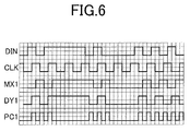
- Fig.6 shows a timing chart of the operation of this embodiment in the lock status.
- the demultiplexer 3 demultiplexes the input data signal DIN into two demultiplexed signals, and the multiplexer 4 multiplexes the demultiplexed data signals into the signal MX1. Accordingly, the phase timing of the output signal MX1 of the multiplexer 4 coincides with that of the clock signal CLK.
- phase comparator 5 By comparing the phase of the output signal MX1 and the phase of the output signal DY1 of the 90-degree delay circuit 1 by the phase comparator 5, a pulse signal PC1 which has a pulse width according to the phase difference is output from the phase comparator 5, DC voltage of this signal is extracted by the lowpass filter 6, and the DC voltage is amplified by the gain control amplifier 7 and is input to the voltage control oscillator 2 as the control voltage.
- the waveform of the output signal of the phase comparator 5 in the timing chart shown in Fig.6 is for a case that the phase comparator is an EXOR type.
- the data signal MX1 the phase timing of which coincides with the phase timing of the output clock signal CLK of the voltage control oscillator 2 is generated, so that the voltage control oscillator 2 is controlled according to a result of phase comparison between the data signal MX1 and the input data signal DIN. Therefore, the phase of the output signal of the voltage control oscillator 2 is determined uniquely in the lock status, so that low jitter can be realized.
- Fig.7 shows an effect of this embodiment.
- bit rate of the input data signal DIN is BR[B/s]
- the jitter is decreased by 1/BR [s]pp.
- Fig.8 shows a second embodiment of the present invention.
- the same numeral is assigned for the same component as that of the first embodiment shown in Fig.5.
- toggle-flip flop circuit (TFF) 8 is connected to input side of the phase comparator 5 as a divider which doubles the minimum pulse width of the output data signal DIN, and the circuit of this embodiment is configured such that the CLK phase timing coincides with that of the output signal FF1 of the toggle-flip flop circuit 8.
- the clock signal CLKm output from the m divider 10 is the recovery divided clock
- the output signals DX21, DX22, ⁇ , DX2N of the demultiplexer 9 are recovery parallel data.
- Fig.9 shows a timing chart of the operation of this embodiment in a lock status.
- a demultiplexer 3 which receives the clock signal CLK demultiplexes the output signal FF1 of the toggle-flip flop circuit 8, and the demultiplexed signals are multiplexed by a multiplexer which uses the clock CLK.
- the phase timing of the output signal MX1 of the multiplexer 4 coincides with that of the clock signal CLK.
- Phases of this signal MX1 and the output signal FF1 of the toggle-flip flop circuit 8 are compared by the phase comparator 5. Then, a signal with pulse width according to the phase difference is output from the phase comparator 5, DC voltage of the pulse is extracted by the lowpass filter 6, and the DC voltage of the pulse is amplified by the gain control amplifier 7 and is input to the voltage control oscillator 2.
- Fig.10 shows a third embodiment of the present invention.
- the same numeral is assigned for the same component as that of the first embodiment shown in Fig.5.
- a delay circuit 11 for delaying the input data signal DIN is inserted, and the output signal DY0 of the delay circuit 11 is delayed by 90-degree by using the 90-degree delay circuit 1.
- a phase comparator 12 which receives the output signal DY0 of the delay circuit 11, the output signal DY1 of the 90-degree delay circuit 1 and the output signal MX1 of the multiplexer 4 is used.
- the phase comparator 12 compares phases of the signal DY1 and the multiplexed signal MX1, and compares the phase of a signal of the comparison result and the phase of the signal DY0 (refer to: Japanese laid-open patent application No.6-252654 for example). According to this phase comparator 12, input-data-pattern dependence of the response can be decreased.
- Phase change of the output signal MX1 of the multiplexer 4 follows phase change of the clock signal CLK, so that the phase comparator 12 outputs a phase comparison signal having a pulse width according to phase timing difference between the clock signal CLK output from the voltage control oscillator 2 and the input data signal DIN.
- Fig.11 shows a fourth embodiment of the present invention.
- the same numeral is assigned for the same component as that of the second and third embodiments shown in Figs.8 and 10.
- a 90-degree delay circuit 1 for receiving the output signal FF1 of the toggle-flip flop circuit 8 is inserted, and a phase comparator 12 which receives the output signal DY1 of the 90-degree delay circuit 1, the output signal FF1 of the toggle-flip flop circuit 8 and the output signal MX1 of the multiplexer 4 is provided instead of the phase comparator 5.
- Fig.12 shows a detailed block diagram of the demultiplexer 3.
- the demultiplexer 3 includes two D-type ms-flip flop circuits 31, 32 which output signals DX11 and DX12 respectively.
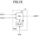
- Fig.13 is a detailed block diagram of the multiplexer 4.
- the multiplexer 4 includes a selector 41 and a clock delay circuit 42.
- the selector 41 is switched by using a signal output from the delay circuit 42 in which the timing of the clock signal CLK is adjusted, so that the signals DX11 and DX12 are selected alternately and outputs MX1. Accordingly, the demultiplexer 3 and the multiplexer 4 can be realized by a simple structure so as to contribute to lowering cost of the clock/data recovery circuit.
- the 90-degree delay circuit 1 shown in Figs.5, 10 and 11 are used for timing adjustment, and this circuit is not limited to the 90-degree delay circuit. Any circuit can be used as long as the circuit performs appropriate phase delay.
- the frequency of the oscillation clock CLK of the voltage control oscillator 2 shown in Figs.5, 8, 10 and 11 in the above-mentioned embodiments is not limited to 1/2 of bit rate of the input data signal DIN.
- the demultiplexer 3 is configured such that it performs 1:K demultiplexing
- the multiplexer 4 is configured such that it performs K:1 multiplexing. That is, the demultiplexer 3 is configured such that the number of parallel expansion becomes K.
- the relationship between the frequency of oscillation clock CLK of the voltage control oscillator 2 (VCO) and the number of parallel expansion of the demultiplexer (DEMUX) is not limited to that shown above.
- Fig.14 shows a general configuration in the first to third examples.
- the 1:M demultiplexer 3 which receives a VCO oscillation clock signal CLK generates a divided signal DCLK by dividing the clock signal CLK by L.
- M parallel data signals are generated by demultiplexing the input signal into M parallel data signals.
- an M:1 multiplexer 4 multiplexes the M parallel data signals and the multiplexed output signal is input to the phase comparator 5.
- DCLK is output as a recovery divided clock and the M parallel signals are output as recovery parallel data.
- the 1:M demultiplexer 3 can be configured by using an 1:2 demultiplexer which receives the clock signal CLK, and two 1:L demultiplexers each of which receives the divided signal DCLK which is generated by dividing the clock signal CLK by L by an L divider.
- the M:1 multiplexer 4 can be configured by using two L:1 multiplexer each of which receives DCLK and a 2:1 multiplexer which receives CLK as shown in Fig.19. In this configuration, the two L:1 multiplexers multiplex the M parallel signals into two parallel signals. Then, the 2:1 multiplexer multiplexes the parallel signals into serial data.
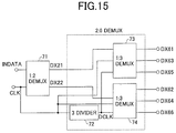
- this 1:6 demultiplexer includes an 1:2 demultiplexer 71, 3 divider 72 (which divides a frequency of a signal by 3) (generally, L divider), and two 1:3 demultiplexers 73 and 74 each of which receives the clock signal DCLK generated by dividing CLK by the 3 divider 72.
- the input data signal INDATA is demultiplexed by the 1:2 demultiplexer 71, and the demultiplexed output signals DX21 and DX22 are demultiplexed by the two 1:3 demultiplexer 73 and 74, so that six parallel signals DX61, DX62, DX63, DX64, DX65 and DX66 are output.
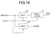
- Fig.16 shows a block diagram of the 1:2 demultiplexer.
- DFFs 75 and 76 DFF1, DFF2 which receives CLK and an inverted signal of CLK respectively discriminate the input data signal.
- output of DFF1 which receives CLK is input into a data latch 77 which uses the inverted signal of CLK, so that phases of the latch output DX21 and output DX22 of the DFF2 which receives the inverted CLK signal are adjusted.
- Fig.17 shows a block diagram of the 1:3 demultiplexer.
- DX21 is input to a shift register which consists of two DFFs 78 and 79 (DFFs 3, 4) which receives the inverted CLK signal.
- DFF5 which receives DCLK discriminates DX21 and outputs a signal DX65
- DFF6 which receives DCLK discriminates an output of DFF3 which is in a first stage of the shift register and outputs DX63
- DFF7 which receives DCLK discriminates an output of DFF4 in a second stage of the shift register and outputs a signal DX61.
- DX22 is input to the 1:3 demultiplexer 74, and, DX62, DX64 and DX66 are output, so that parallel signals DX61, DX62, DX63, DX64, DX65 and DX66 are obtained.
- FIG.18 A timing chart of this 1:6 demultiplexer is shown in Fig.18.
- each DFF and data latch performs rewriting operation at rising edge of the clock.
- Fig.19 shows a block diagram of a 6:1 multiplexer.
- the 6:1 multiplexer includes two 3:1 multiplexers 81, 82 each of which receives DCLK, and a 2:1 multiplexer 83.
- the signals DX61, DX62, DX63, DX64, DX65 and DX66 are multiplexed by two 3:1 multiplexers 81, 82, and the multiplexed outputs MX21 and MX22 are multiplexed by the 2:1 multiplexer 83 which receives CLK, so that serial data MX61 (MUXOUT) is output.
- Fig.20 shows a block diagram of the 3:1 multiplexer 81.
- DX65 is input to DFF8 (84) which receives CLK
- DFF8 and DX63 are input to a 2:1 selector 1 (85) which receives an output PG3 of a pulse generator 89 which outputs the signal with pulse width of CLK at DCLK period.
- the output of the 2:1 selector 1 is input to DFF9 (86) which receives DCLK
- the output of DFF9 and DX1 are input to a 2:1 selector 2 (87) which receives PG3 as a switching signal
- the output of the 2:1 selector 2 is input to DFF10 (88) which receives an inverted signal of CLk.
- DX61, DX63 and DX65 are multiplexed, so that MX21 is output.
- DX62, DX64 and DX66 are multiplexed by the 3:1 multiplexer 82 and MX22 is output as a multiplexed output.
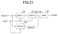
- Fig.21 shows a block diagram of the pulse generator 89.
- an inverted signal of DCLK is input to DFF11 (90) which receives an inverted signal of CLK as a clock signal, and the output is input to DFF12 (91) which receives CLK as a clock signal.
- the output signal of DFF12 and an output signal of DFF13 are input to an NOR circuit 92 in which the output signal of DFF12 is a signal generated by delaying the inverted signal of DCLK by one period of CLK, and the output signal of DFF13 is a signal generated by delaying an opposite signal of DCLK by a half period of CLK.
- the NOR circuit 92 outputs the signal PG3 of the pulse generator which outputs the signal with pulse width of CLK at DCLK period.
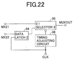
- Fig.22 shows a block diagram of a 2:1 multiplexer.
- MX22 is input to a data latch 2 (94) which receives CLK, so that the phase of MX22 is shifted by a half period of CLK.
- the data latch output signal and MX21 are input to a 2:1 selector 3 (95) which receives an inverted signal of a signal output from a timing adjustment circuit 96 in which timing of CLK is adjusted as a switching signal.
- MX21 and the output of the data latch are output alternately, so that a serial data signal MUXOUT in which MX21 and MX22 are multiplexed is output.
- a timing chart of the 6:1 multiplexer is shown in Fig.23.
- DFF8, 9, 10, 11, 12 and 13 perform rewriting operation at rising edge of the clock signal
- the 2:1 selectors 1 and 2 select DX63 and DX61 when PG3 is 1 (high), and select DFF output when PG3 is 0 (low).
- the switching signal of the 2:1 selector 3 is a signal in which CLK is delayed, and the 2:1 selector 3 selects MX21 when it is 0 (low), selects output of the data latch 2 when it is 1 (high).
- the 1:M demultiplexer can be configured as shown in Fig.24.
- an input data signal is demultiplexed by an 1:2 demultiplexer 97 which uses CLK as a clock signal into two parallel data signals.
- the parallel signals are demultiplexed into four parallel signals by second and third 1:2 demultiplexers 99, 100 which receive a divided signal DCLK2 divided by 2 by a 2 divider 98.
- 1:2 T demultiplexing is performed. Accordingly, the input data signal is demultiplexed into 2 T parallel data signals.
- the configuration of the M:1 multiplexer 4 is as shown in Fig.25.
- the demultiplexed signals are multiplexed into M/2 parallel data signals by M/2 2:1 multiplexers each of which receives DCLK2 T-1 generated by dividing CLK by L as a clock signal.
- the multiplexed data signals are multiplexed repeatedly by using 2:1 multiplexers which use a divided clock by using parallel signal input number.
- a serial data signal is output.
- DCLK2 T-1 is output as a recovery divided clock and M parallel signals are output as recovery parallel data.
- the 1:M demultiplexer can be configured by an 1:K demultiplexer and K 1:L demultiplexers.
- the 1:K demultiplexer demultiplexes input data signal into K parallel data signals by using the generated signal and CLK.
- the M:1 multiplexer can be configured by K L:1 multiplexers and a K:1 multiplexer.
- the L:1 multiplexers multiplexe M parallel signals into K parallel signals by using DCLK and CLK, and the K parallel signals are multiplexed into a serial data signal by using CLK and MCLK generated by multiplying CLK by J by using a multiplier.
- the configuration can be the same as that of the first embodiment.
- K is an odd number equal to or larger than 3
- M K ⁇ L (L is an integer equal to or larger than 1)
- the circuit can be configured as shown in Fig.26.
- MCLK multiplied signal
- a divided clock signal generated by multiplying CLK by S and M parallel data signals are output.
- the division number of the divider and the division number of VCO can take various relationship. In the following description, it is assumed that the division number of the divider is Q, the dividing ratio of the oscillation frequency of VCO to the bit rate of the input data signal is K and the number of parallel expansion of the second demultiplexer (DEMUX 9) is N.
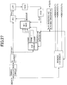
- a configuration which generalizes the configuration of Fig.8 is shown in Fig.27
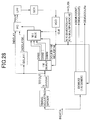
- a configuration which generalizes the configuration of Fig.11 is shown in Fig.28.
- multiplexing/demultiplexing is performed on the input data signal to convert the signal into a data signal in which the phase is corresponds with that of an output clock signal of the voltage control oscillator. Then, by comparing phases of the data signal and the input data signal, phase comparison output signal according to phase difference between the input data signal and the data signal can be output even by using the voltage control oscillator the frequency of which is 1/k of that of the conventional voltage control oscillator.
- low jitter can be realized such that the feedback voltage to the voltage control oscillator can be proportional to the difference between the value of two times of the free-running frequency of the voltage control oscillator and the value of bit rate of the input data.
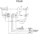
- Fig.29 shows an example of a clock/data recovery circuit (CDR circuit) in the embodiments which have been described.
- 1 indicates a delay circuit which delays the input data signal DIN for timing adjustment
- 2 indicates a voltage control oscillator (VCO) which oscillates at a frequency of 1/2 of the bit rate of the input data signal DIN
- 3 indicates a demultiplexer (DEMUX) which performs 1:N (N ⁇ 2) demultiplexing operation for the input data signal DIN by using a clock signal CLK output from the voltage control oscillator
- 4 indicates a multiplexer (MUX) which performs N:1 multiplexing operation for the N output signals DX1,DX2, ⁇ ,DXN from the demultiplexer 3 by using the clock signal CLK as a clock signal
- 5 indicates an phase comparator (PC) which compares the output signal MX1 of the multiplexer 4 and the output signal of the delay circuit
- 6 indicates a lowpass filter (LPF) which extracts DC voltage from the output signal of the phase comparator
- 7 indicates a gain control amplifier (GCA) which amplifies the output signal of the lowpass filter 6 and inputs the ampl
- the output signal of the m divider 408 is a recovery divided clock CLKm.
- the output signals DX1, DX2, ⁇ , DXN of the demultiplexer 3 are data signals which are recovery parallel data.
- the demultiplexer 3 demultiplexes the input data signal DIN into N, and the multiplexer 4 multiplexes the N demultiplexed data signals into MX1. Accordingly, the phase timing of the output signal MX1 of the multiplexer 4 coincides with that of the clock signal CLK.
- the phase comparator 5 By comparing the phase of the output signal MX1 and the phase of the output signal of the delay circuit 1 by the phase comparator 5, a pulse signal which has a time width according to the phase difference is output from the phase comparator 5, DC voltage of this signal is extracted by the lowpass filter 6, and the DC voltage is amplified by the gain control amplifier 7 and is input to the voltage control oscillator 2 as the control voltage.
- signals which can be output from the clock/data recovery circuit are only the signal MX1, N parallel signals DX1, DX2, ⁇ , DXN which are 1:N demultiplexed, and a clock signal CLKm having a frequency of equal to or less than 1/2 of the bit rate of the input data signal.
- the circuit can not output a clock signal (serial clock signal) having the same frequency of the input bit rate.
- Fig.30 is a block diagram of the clock/data recovery circuit of the eighth embodiment of the present invention.
- 1 indicates a delay circuit which delays the input data signal DIN for timing adjustment
- 2 indicates a voltage control oscillator (VCO) which oscillates at a frequency of 1/2 of the bit rate of the input data signal DIN
- 3 indicates a demultiplexer (DEMUX) which performs 1:N (N ⁇ 2) demultiplexing operation for the input data signal DIN by using a clock signal CLK output from the voltage control oscillator
- 4 indicates a multiplexer (MUX) 5 which performs N:1 multiplexing operation for the N output signals DX1, DX2, ⁇ ,DXN from the demultiplexer 3 by using the clock signal CLK as a clock signal
- 5 indicates an phase comparator (PC) including EXOR and the like which compares the output signal MX1 of the multiplexer 4 and the output signal of the delay circuit
- 6 indicates a lowpass filter (LPF) which extracts DC voltage from the output signal of the
- 409 indicates a 90-degree delay circuit which delays the clock signal CLK by 90 degree
- 410 indicates a multiplier which multiplies an output clock signal CLK90 of the 90-degree delay circuit 409 and the clock signal CLK, and outputs a clock signal CLK1.
- Fig.30 Difference between configurations of Fig.30 and Fig.29 is that the 90-degree delay circuit 409 and the multiplier 410 are added. Therefore, in the configuration shown in Fig.30, same operation as that shown in Fig.29 is performed in the same parts as Fig.29.
- the circuit shown in Fig.30 outputs the clock signal CLKm from the m divider 408 and the output signals DX1,DX2, ⁇ , DXN of the demultiplexer 3 as parallel signals.
- Fig.36 shows input-output waveforms of the multiplier 410.
- CLK1 output from the multiplier 10 can be represented as
- the period Tl(sec) of the output clock signal CLK1 of the multiplier 410 is 1/2 of the period T of the output clock signal CLK of the voltage control oscillator 2, the frequency of the clock signal CLK1 becomes the same as the bit rate of the input data signal DIN.
- a serial output signal including the clock signal CLK1 having the same frequency of the bit rate of the input data signal and the discriminated data signal MX1 of the same bit rate of that of the input data signal can be output in addition to the parallel output signals including the divided clock signal CLKm and the output signals DX1, DX2, ⁇ ,DXN.
- Fig.31 is a block diagram of the clock/data recovery circuit of the ninth embodiment of the present invention.
- the same numeral is assigned to the same component as that of Fig.30.
- a voltage control oscillator 421 is adopted in which the voltage control oscillator 421 outputs the clock signal CLK of the frequency of 1/2 of bit rate of the input data signal DIN and the clock signal CLK90 of which phase is shifted by 90 degree (that is, they are quadrature).
- Both of the clock signals CLK and CLK90 are input to the multiplier 410, so that the multiplier 41 outputs the clock signal CLK1 having a frequency which is two times of that of the clock signal CLK.
- Other parts are the same as those in Fig.30.
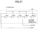
- Fig.37 shows the configuration of the voltage control oscillator 421.
- the voltage control oscillator 421 is configured such that buffer circuits B1,B2, ⁇ ,Bk,Bk+1,Bk+2, ⁇ ,B2k of 2k (k ⁇ 1) stages each having the same delay time are connected in series.
- the inverted signal of the output of the buffer B2k of the 2kth (the last stage) is input to the buffer B1 of the first stage (ring oscillator type VCO).
- the clock signal CLK is a signal input to the first stage buffer circuit
- the clock signal CLK90 the phase of which is shifted by 90 degree is an output of the buffer circuit Bk of the kth stage.
- the control voltage output from the gain control amplifier 7 controls the delay time tpd at the same time by controlling switching current of each buffer circuit.
- the 90-degree delay circuit 409 as shown in Fig.30 is not necessary, so that simplified clock/data recovery circuit can be realized.
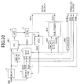
- Fig.32 is a block diagram of the clock/data recovery circuit of the tenth embodiment of the present invention.
- the same numeral is assigned to the same component as that of Fig.30.
- the output of the delay circuit 1 which delays the input data signal DIN is divided into two branches, and a 90-degree delay circuit 11 is connected to one of the branches.
- a phase comparator 451 which compares phases of another signal of the branches output from the delay circuit 1, the output signal of the 90-degree delay circuit 11 and the output signal MX1 of the multiplexer 4 is adopted.
- phase comparator 451 phase comparison between the output signal of the 90-degree delay circuit 11 and the output signal MX1 of the multiplexer 4 is performed first. Then, the result of the phase comparison and the output signal of the delay circuit 1 are compared (for example, Japanese laid-open patent application No. 5-56410). According to this phase comparator 451, input-data-pattern dependence of the response can be decreased.
- phase change of the output signal MX1 of the multiplexer 4 follows the phase change of the clock signal CLK.
- the phase comparator 451 outputs a phase comparison signal having a pulse width according to phase differences between the phase of MX1 and the phase of the input data signal DIN.
- Fig.33 is a block diagram of the clock/data recovery circuit of the eleventh embodiment of the present invention.
- the same numeral is assigned to the same component as that of Fig.30.
- the output of the delay circuit 1 which delays the input data signal DIN is divided into two branches, and a 90-degree delay circuit 11 is connected to one of the branches.
- a phase comparator 451 receives another signal of the branches output from the delay circuit 1, the output signal of the 90-degree delay circuit 11 and the output signal MX1 of the multiplexer 4.
- a voltage control oscillator 421 is adopted in which the voltage control oscillator 421 outputs the clock signal CLK of the frequency of 1/2 of bit rate of the input data signal DIN and the clock signal CLK90 the phase of which is shifted by 90 degree. Both of the clock signals CLK and CLK90 are input to the multiplier 410, so that the multiplier 410 outputs the clock signal CLK1 having a frequency which is two times of the clock signal CLK.
- Fig.34 is a block diagram of a clock/data recovery circuit of the twelfth embodiment of the present invention.
- the same numeral is assigned to the same component as that of Fig.30.
- the clock signal CLK output from the voltage control oscillator 2 is input to a PLL type clock multiplier 412, so that the clock signal CLK1 having the frequency of two times of that of the clock signal CLK is output.
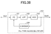
- Fig.38 is a block diagram of an inside configuration of the PLL type clock multiplier 412.
- This multiplier 412 includes a phase comparator 121 which compares phases of the clock signal CLK and the output signal of the 2 divider 124, a lowpass filter 122 which extracts DC voltage from the output signal of the phase comparator 121, a voltage control oscillator 123 which oscillates the clock signal CLK1 by using the output signal of the lowpass filter 122 as a control voltage, and the 2 divider 124 which divides the frequency of the output clock signal CLK1 of the voltage control oscillator 123 into 1/2 frequency.
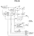
- Fig.35 is a block diagram of the clock/data recovery circuit of the thirteenth embodiment of the present invention.
- the same numeral is assigned to the same component as that of Fig.30.
- the output of the delay circuit 1 which delays the input data signal DIN is divided into two branches, and a 90-degree delay circuit 11 is connected to one of the branches.
- a phase comparator 451 receives another signal of the branches output from the delay circuit 1, the output signal of the 90-degree delay circuit 11 and the output signal MX1 of the multiplexer 4.
- the PLL type clock multiplier 412 is adopted in which the clock signal CLK output from the voltage control oscillator 2 is input to the PLL type clock multiplier 412, so that the clock signal CLK1 having the frequency of two times of that of the clock signal CLK is generated.
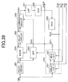
- FIG.39 Another example of the CDR circuit using the discriminator consisting of DEMUX and MUX described in the above-mentioned embodiments is shown in Fig.39.
- 201 indicates a first delay circuit which delays the input data signal DIN
- 202' indicates a discriminator including an 1:2 demultiplexer 221 and a 2:1 multiplexer 222
- 203 indicates a D-type ms-flip flop circuit which discriminates an output data signal DY1 of the delay circuit 201 by using the output data signal DF1 of the discriminator 202'
- 204 indicates a phase comparator of EXOR type which compares phases of the output data signal DY1 of the delay circuit 201 and the output data signal DF1 of the discriminator 202'
- 205 indicates a second delay circuit which delays an output signal PC1 of the phase comparator 204
- 206 indicates a combining circuit which receives the output signal DY2 of the delay circuit 205 and the output data signal DF2 of the D-type ms-flip flop circuit 203 and outputs a pulse signal COM1 (three value) of +1, -1 or 0,
- 207 indicates a lowpass filter (LPF) which extracts
- the 1:2 demultiplexer 221 demultiplexes the input data signal DIN into two parallel demultiplexed data signals DX1 and DX2, and the multiplexer 222 multiplexes the data signals DX1 and DX2 into a serial data signal DF1.
- the phase comparator 204 outputs a signal PC1 having a pulse width corresponding to phase difference between the data DF1 discriminated by the circuit 202' and the output data DY1 of the delay circuit 201.
- the D-type ms-flip flop circuit 203 outputs a signal of 0 when the output signal DF1 of the circuit 202' leads the output signal DY1 of the delay circuit 201
- the D-type ms-flip flop circuit 203 outputs a signal of 1 when the output signal DF1 of the circuit 202' lags the output signal DY1 of the delay circuit 201. That is, decision of lead/lag of phase is performed in the D-type ms-flip flop circuit 203 and the phase comparator 204 detects lead/lag magnitude of the phase.
- the combining circuit 206 combines the signal DY2 generated by delaying the output signal PC1 of the phase comparator 204 by the delay circuit 205 and the output signal DF2 of the D-type ms-flip flop circuit 203.
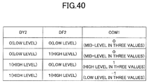
- the combining circuit 206 operates as shown in Fig.40, so that it outputs a pulse signal COM1 of three value of +1, -1 or 0. That is, when the clock signal CLK leads the input data signal DIN, the combining circuit 206 outputs a signal of 1 having a pulse width which is proportionate to the magnitude of lead. When the clock signal CLK lags the input data signal DIN, the combining circuit 206 outputs a signal of -1 having a pulse width which is proportionate to the magnitude of lag. When the output from the phase comparator 204 is 0 (there is no phase comparison information), the combining circuit 206 outputs a signal of 0.
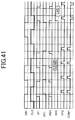
- Fig. 41 shows a timing chart of the above operation. According to this embodiment, since decision of lead/lag of phase and detection of lead/lag magnitude are performed by different circuits respectively, phase margin becomes large, so that synchronization operation (pull-in operation) is stabilized.
- Fig.42 shows a circuit diagram indicating an inside configuration of the combining circuit 206. Differential input is assumed in Fig.42.
- the combining circuit 206 includes transistors Q1, Q2 which form a first ECL circuit, transistors Q3, Q4 which form a second ECL circuit, transistors Q5, Q6 which form a third ECL circuit, a load resistance R2 common for the transistors Q2, Q4, and first and second current sources I1, I2.
- a common emitter of the transistors Q1, Q2 is connected to a collector of the transistor Q5 and the current source I1
- a common emitter of the transistors Q3,Q4 is connected to a collector of the transistor Q6
- a common emitter of the transistors Q5,Q6 is connected to the current source I2.
- a non-inverted signal of the output signal DF2 of the D-type ms-flip flop circuit 203 is input into a base of the transistors Q1, Q4, the inverted signal of DF2 is input to a base of the transistors Q2, Q3.
- a non-inverted signal of the output signal DY2 of the delay circuit 5 is input into a base of the transistor Q5, the inverted signal of DY2 is input to a base of the transistor Q6.
- the 1:2 demultiplexer 221 and the 2:1 multiplexer 222 which form the circuit 202' perform demultiplexing and multiplexing by using the clock signal CLK
- the frequency of the clock signal CLK can be 1/2 of the bit rate of the input data signal DIN. That is, operation speed required for the voltage control oscillator 208 can be lowered, so that speedup becomes available.
- the demultiplexer 221 By configuring the demultiplexer 221 to perform 1:N demultiplexing and the multiplexer 222 to perform N:1 multiplexing, since the frequency required for the clock signal CLK becomes 1/N, further speedup becomes possible, so that the bit rate of input data signal to which the clock/data recovery circuit can achieve lock can be further increased.
- the configurations of the sixth embodiments can be adopted. According to this embodiment, phase margin for phase comparison is extended, so that pull-in operation using higher frequency is stabilized. In addition, by adopting demultiplexing and multiplexing, pull-in operation using further higher frequency is stabilized.
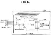
- Fig.44 shows a receiving apparatus 300 which includes a CDR circuit of the present invention.
- the receiving apparatus 300 is used in high speed optical communication and the like.
- the input optical data signal is optical-to-electrical converted by an optical/electrical converter which includes a photo detector 301, and electrical signal level and the amplitude of the converted output are adjusted by the AGC amplifier and the limiting amplifier 302.
- the signal is input to the CDR circuit 303 of the present invention, and the parallel signals (demultiplexed signals) and divided clock signal are output.
- a transmission apparatus can be configures in which the parallel signals (demultiplexed signals) and divided clock signal are input to the signal processing circuit 304, and the output of the signal processing circuit is input to a sending apparatus, and a signal is output to the outside.
- the input data signal is converted into a data signal in which the phase corresponds with that of the output clock signal of the voltage control oscillator by performing demultiplexing/multiplexing operation.
- the phase comparison signal according to the phase difference can be output even when the frequency of voltage control oscillator is 1/2 of that of the conventional circuit, and the feedback voltage to the voltage control oscillator becomes a voltage according to phase difference.
- low jitter can be realized.
- a clock signal is provided to the 1:2 DEMUX via a TFF which decreases the frequency of the clock output from VCO oscillating at frequency same as bit rate of input data to 1/2.
- operating margin of the discriminator is increased.
- the VCO oscillates at the same frequency as the bit rate of the input data high speed operation is required for the circuits forming the VCO and circuits forming the TFF.
- high speed signals are transmitted in signal lines between VCO-TFF.
- operation of CDR+DEMUX is limited to the performance of operation of the VCO and TFF.
- a problem that the high speed signals between VCO-TFF are sensitive to noise leaking from other circuits arises.
- the discriminator is configured by the 1:2 demultiplexer and the 2:1 multiplexer and the VCO oscillates at a speed of 1/2 of that of the conventional VCO.
- the discriminator can be used as demultiplexed data output, and the DEMUX clock output can be used as VCO output. Therefore, the last stage 1:2 DEMUX shown in Fig.4 becomes unnecessary and reduction of power requirements can also be realized.
- the input data signal phase is converted to VCO clock signal phase according to the present invention.
- the phase comparator can perform linear comparison between the input data signal and DEMUX+MUX output signal.
- the phase comparator outputs a signal having a pulse width proportionate to phase difference between the input data signal and data signals the phase timing of which coincides with that of VCO clock signal.
- the analog component of the phase comparison signal is fed back to the VCO, so that synchronization status of PLL can be realized.
- this linear phase comparison method the effect of jitter decreasing can be obtained.
- the low jitter, small and low power consumption clock/data recovery circuit can be realized in which the clock/data recovery circuit is used as an optical front end circuit receiver and the like in a router or in a cross connect switch in SDH/SONET, point to point transmission, GbE/10GbE and Fiber Channel in an optical communication system.
- the clock/data recovery circuit is used as an optical front end circuit receiver and the like in a router or in a cross connect switch in SDH/SONET, point to point transmission, GbE/10GbE and Fiber Channel in an optical communication system.
Landscapes
- Engineering & Computer Science (AREA)
- Computer Networks & Wireless Communication (AREA)
- Signal Processing (AREA)
- Microelectronics & Electronic Packaging (AREA)
- Synchronisation In Digital Transmission Systems (AREA)
- Time-Division Multiplex Systems (AREA)
Abstract
Description
and an input of the first stage buffer circuit is the clock signal and an output of kth stage buffer circuit is the quadrature clock signal.

Claims (18)
- A clock/data recovery circuit characterized by:wherein said clock/data recovery circuit outputs said clock signal generated by said voltage control oscillator as a recovery divided clock signal, and outputs said M demultiplexed signals from said demultiplexer as recovery parallel data signals.a voltage control oscillator for generating a clock signal of a frequency of 1/K (K=2,3,···) of a bit rate of an input data signal;a delay circuit for delaying said input data signal for timing adjustment;a demultiplexer for demultiplexing said input data signal into M demultiplexed signals (M=2,3,···) by using said clock signal;a multiplexer for multiplexing said M demultiplexed signals by using said clock signal;a phase comparator for comparing phases of an output signal of said delay circuit and an output signal of said multiplexer;a lowpass filter for extracting DC voltage from an output signal of said phase comparator and for inputting said DC voltage to said voltage control oscillator as a control voltage;
- The clock/data recovery circuit as claimed in claim 1, wherein M=K×L in which L is a natural number.
- The clock/data recovery circuit as claimed in claim 1, said clock/data recovery circuit comprising:another delay circuit, provided before said delay circuit, for delaying said input data signal; andanother phase comparator, instead of said phase comparator, for comparing phases of said output signal of said delay circuit and said output signal of said multiplexer, and comparing phases of a result of comparison of phases of said output signal of said delay circuit and said output signal of said multiplexer and an output signal of said another delay circuit.
- The clock/data recovery circuit as claimed in claim 1, when K=2 and M=2, said demultiplexer comprising:a first D-type ms-flip flop circuit for receiving said input data signal by using said clock signal; anda second D-type ms-flip flop circuit for receiving said input data signal by using an inverted signal of said clock signal;said multiplexer comprising:a clock delay circuit for delaying said clock signal; anda selector for selecting alternately an output signal of said first D-type ms-flip flop circuit and an output signal of said second D-type ms-flip flop circuit by using an output signal of said clock delay circuit.
- The clock/data recovery circuit as claimed in claim 2, when K=2, said demultiplexer comprising:a first demultiplexer for demultiplexing said input data signal into two first parallel data signals by using said clock signal;two second demultiplexers each of which demultiplexes one of said first parallel signals into L second parallel data signals by using a divided clock signal generated dividing said clock signal by L and said clock signal;said multiplexer comprising:two first multiplexers each of which multiplexes said L second parallel data signals into serial data by using said divided clock signal and said clock signal; anda second multiplexer for multiplexing two parallel data signals output from said two first multiplexer into serial data by using said clock signal.
- The clock/data recovery circuit as claimed in claim 2, when K=2 and M=2T (T is an integer equal to or larger than 2), said demultiplexer comprising:T stages in which a Qth (Q=1,2,3···T) stage includes 2(Q-1) 1:2 demultiplexers, and a divided clock signal generated by dividing said clock signal by 2(Q-1) is provided to each 1:2 demultiplexer in said Qth stage;said multiplexer comprising:T stages in which a Qth (Q=1,2,3···T) stage includes 2(T-Q) 2:1 multiplexers, a divided clock signal generated by dividing said clock signal by 2(T-Q) is provided to each 2:1 multiplexer.
- The clock/data recovery circuit as claimed in claim 2, when K>2, said demultiplexer comprising:a part for generating K-1 signals in which phases are different each other with respect to said clock signal;a first demultiplexer for demultiplexing said input data signal into K first parallel data signals by using said K-1 signals and said clock signal; andK second demultiplexers each of which demultiplexes one of said first parallel data signals into L second parallel data signals;said multiplexer comprising:K first multiplexer each of which multiplexes said L second parallel data signals into serial data by using said divided clock signal and said clock signal; anda second multiplexer for multiplexing K parallel data signals output from said K first multiplexers into serial data by using a multiplied signal generated by multiplying said clock signal and said clock signal.
- A clock/data recovery circuit characterized by:wherein said clock/data recovery circuit outputs an output signal of said m (=N/K) divider as a recovery divided signal, and outputs said N demultiplexed signals output from said second demultiplexer as recovery parallel data signals.a voltage control oscillator for generating a clock signal of a frequency of 1/K (K=2,3,···) of a bit rate of an input data signal;a Q divider for receiving said input data signal and for dividing a frequency of said input data signal by Q (Q=2,3,4···);a first demultiplexer for demultiplexing an output signal of said Q divider into M demultiplexed signals (M=2,3,···) by using said clock signal;a second demultiplexer for demultiplexing said input data signal into N demultiplexed signals by using said clock signal;a multiplexer for multiplexing said M demultiplexed signals output from said first demultiplexer into a signal by using said clock signal;a phase comparator for comparing phases of an output signal of said Q divider and an output signal of said multiplexer;a lowpass filter for extracting DC voltage from an output signal of said phase comparator and for inputting said DC voltage to said voltage control oscillator as a control voltage; andan m (=N/K) divider for dividing a frequency of an output clock signal of said voltage control oscillator by m;
- The clock/data recovery circuit as claimed in claim 8, wherein M=K×L in which L is a natural number.
- The clock/data recovery circuit as claimed in claim 8, said clock/data recovery circuit comprising:a delay circuit provided after said Q divider (Q=2,3,4···) ; andanother phase comparator, instead of said phase comparator, for comparing phases of an output signal of said delay circuit and said output signal of said multiplexer, and comparing phases of a result of comparison of phases of said output signal of said delay circuit and said output signal of said multiplexer and an output signal of said Q divider.
- The clock/data recovery circuit as claimed in claim 8, when K=2 and M=2, said first demultiplexer comprising:a first D-type ms-flip flop circuit for receiving an output signal of said Q divider by using said clock signal; anda second D-type ms-flip flop circuit for receiving an output signal of said Q divider by using an inverted signal of said clock signal;said multiplexer comprising:a clock delay circuit for delaying said clock signal; anda selector for selecting alternately an output signal of said first D-type ms-flip flop circuit and an output signal of said second D-type ms-flip flop circuit by using an output signal of said clock delay circuit.
- The clock/data recovery circuit as claimed in claim 1, when K=2, said clock/data recovery circuit comprising:wherein said clock/data recovery circuit outputs a data signal from said multiplexer and a clock signal from said multiplier as a serial data signal.an m (=M/K) divider for outputting a divided clock signal generated by dividing said clock signal by m;a 90-degree delay circuit for delaying said clock signal output from said voltage control oscillator by 90 degree; anda multiplier for multiplying an output signal from said 90-degree delay circuit and a clock signal output from said voltage control oscillator, and outputting a clock signal the frequency of which is the same as bit rate of said input data signal;
- The clock/data recovery circuit as claimed in claim 3, when K=2, said clock/data recovery circuit comprising:wherein said clock/data recovery circuit outputs a data signal from said multiplexer and a clock signal from said multiplier as a serial data signal.an m(=M/K) divider for outputting a divided clock signal generated by dividing said clock signal by m;a 90-degree delay circuit for delaying said clock signal output from said voltage control oscillator by 90 degree; anda multiplier for multiplying an output signal from said 90-degree delay circuit and a delay clock signal from said voltage control oscillator, and outputting a clock signal of which the frequency is the same as bit rate of said input data signal;
- The clock/data recovery circuit as claimed in claim 12, instead of providing said 90-degree delay circuit, wherein said voltage control oscillator outputs a quadrature clock signal having the same frequency as said clock signal and being quadrature to said clock signal, said multiplier receives said clock signal and said quadrature clock signal and outputs a clock signal having the same frequency as bit rate of said input data signal.
- The clock/data recovery circuit as claimed in claim 1, said clock/data recovery circuit comprising:wherein said clock/data recovery circuit outputs a data signal from said multiplexer and a clock signal from said K multiplier as a serial data signal.an m divider for outputting a divided clock signal generated by dividing said clock signal by m; anda K multiplier for multiplying said clock signal by K, so that a clock signal having the same frequency as bit rate of said input data signal is output;
- The clock/data recovery circuit as claimed in claim 14, said voltage control oscillator comprising 2k (k≧1) buffer circuits having the same delay time in which said delay time is controlled by a control voltage, said buffer circuits being connected in series, an inverted signal of the output of a 2kth buffer circuit is input to a first stage buffer circuit;
wherein an input of said first stage buffer circuit is said clock signal and an output of kth stage buffer circuit is said quadrature clock signal. - The clock/data recovery circuit as claimed in claim 15, said K multiplier comprising:wherein said first phase comparator receives an output signal of said K divider and said clock signal of said voltage control oscillator, and said first voltage control oscillator outputs a clock signal having the same frequency as bit rate of said input data signal.a first phase comparator,a lowpass filter for extracting DC voltage from an output signal of said first phase comparator;a first voltage control oscillator in which the oscillation frequency is controlled by an output signal of said first lowpass filter; anda K divider for dividing an output signal of said first voltage control oscillator by K
- A receiving apparatus including a clock/data recovery circuit, said clock/data recovery circuit characterized by:wherein said clock/data recovery circuit outputs said clock signal generated by said voltage control oscillator as a recovery divided clock signal, and outputs said M demultiplexed signals output from said demultiplexer as recovery parallel data signals.a voltage control oscillator for generating a clock signal of a frequency of 1/K (K=2,3,···) of a bit rate of an input data signal;a delay circuit for delaying said input data signal for timing adjustment;a demultiplexer for demultiplexing said input data signal into M demultiplexed signals (M=2,3,···) by using said clock signal;a multiplexer for multiplexing said M demultiplexed signals by using said clock signal;a phase comparator for comparing phases of an output signal of said delay circuit and an output signal of said multiplexer;a lowpass filter for extracting DC voltage from an output signal of said phase comparator and inputting said DC voltage to said voltage control oscillator as a control voltage;
Applications Claiming Priority (4)
| Application Number | Priority Date | Filing Date | Title |
|---|---|---|---|
| JP2001063775 | 2001-03-07 | ||
| JP2001063775 | 2001-03-07 | ||
| JP2001326090 | 2001-10-24 | ||
| JP2001326090 | 2001-10-24 |
Publications (3)
| Publication Number | Publication Date |
|---|---|
| EP1239627A2 true EP1239627A2 (en) | 2002-09-11 |
| EP1239627A3 EP1239627A3 (en) | 2005-11-30 |
| EP1239627B1 EP1239627B1 (en) | 2009-02-25 |
Family
ID=26610796
Family Applications (1)
| Application Number | Title | Priority Date | Filing Date |
|---|---|---|---|
| EP02251533A Expired - Lifetime EP1239627B1 (en) | 2001-03-07 | 2002-03-05 | Clock/Data recovery circuit |
Country Status (4)
| Country | Link |
|---|---|
| US (1) | US7095816B2 (en) |
| EP (1) | EP1239627B1 (en) |
| CA (1) | CA2374777C (en) |
| DE (1) | DE60231266D1 (en) |
Cited By (2)
| Publication number | Priority date | Publication date | Assignee | Title |
|---|---|---|---|---|
| EP1276270A3 (en) * | 2001-07-09 | 2004-05-12 | Alcatel | Method and arrangement for recovering a clock signal from a data signal |
| EP2755350A1 (en) * | 2013-01-15 | 2014-07-16 | Alcatel-Lucent | Apparatus for performing clock and/or data recovery |
Families Citing this family (15)
| Publication number | Priority date | Publication date | Assignee | Title |
|---|---|---|---|---|
| JP4426739B2 (en) * | 2001-06-26 | 2010-03-03 | 日本オプネクスト株式会社 | Optical module and manufacturing method thereof |
| US6862397B2 (en) * | 2002-10-15 | 2005-03-01 | The Boeing Company | Method for audibly measuring optical efficiency in an installed fiber optic link |
| EP1471667B1 (en) * | 2003-04-22 | 2005-09-07 | Alcatel | Clock recovery from distorted optical signals |
| DE102004047871A1 (en) * | 2004-10-01 | 2006-04-06 | Deutsche Thomson-Brandt Gmbh | Signal input circuit |
| KR100607858B1 (en) * | 2004-12-31 | 2006-08-08 | 삼성전자주식회사 | Apparatus and method for removing noise of frequency band used in mobile communication terminal |
| US7861105B2 (en) * | 2007-06-25 | 2010-12-28 | Analogix Semiconductor, Inc. | Clock data recovery (CDR) system using interpolator and timing loop module |
| JP2009094638A (en) * | 2007-10-04 | 2009-04-30 | Yokogawa Electric Corp | High frequency module |
| WO2012070073A1 (en) * | 2010-11-23 | 2012-05-31 | Power-One Italy S.P.A. | Method and circuit for clock recovery of a data stream description |
| US8755480B1 (en) | 2011-12-30 | 2014-06-17 | Altera Corporation | Integrated circuit (IC) clocking techniques |
| US9166605B2 (en) * | 2013-03-18 | 2015-10-20 | Terasquare Co., Ltd. | Low-power and all-digital phase interpolator-based clock and data recovery architecture |
| US10212006B2 (en) * | 2016-03-01 | 2019-02-19 | Mediatek Inc. | Feed-forward filtering device and associated method |
| KR102653891B1 (en) | 2016-11-30 | 2024-04-02 | 삼성전자주식회사 | Phase interpolator for interpolating delayed clock signal and device including the same for operating data sampling by using phase interpolated clock signal |
| CN108322212B (en) * | 2018-05-14 | 2024-08-16 | 广东工业大学 | A high-speed and low-power four-to-five prescaler |
| TWI768690B (en) * | 2021-01-29 | 2022-06-21 | 瑞昱半導體股份有限公司 | Reference-less clock and data recovery (cdr) device and method thereof |
| CN113300702B (en) * | 2021-05-24 | 2023-03-24 | 成都振芯科技股份有限公司 | Signal jitter separation circuit and method |
Family Cites Families (13)
| Publication number | Priority date | Publication date | Assignee | Title |
|---|---|---|---|---|
| JPH0693667B2 (en) * | 1988-08-03 | 1994-11-16 | 富士通株式会社 | Synchronous multiplexing |
| JPH0556410A (en) | 1991-08-28 | 1993-03-05 | Fujitsu General Ltd | Television receiver |
| JP3196949B2 (en) | 1993-02-23 | 2001-08-06 | 日本電信電話株式会社 | Data signal phase comparison circuit |
| JP3481051B2 (en) * | 1996-06-19 | 2003-12-22 | 富士通株式会社 | Charge pump circuit, PLL circuit having the charge pump circuit, and semiconductor integrated circuit |
| JP2862078B2 (en) | 1996-10-18 | 1999-02-24 | 日本電気株式会社 | PLL |
| US5933058A (en) * | 1996-11-22 | 1999-08-03 | Zoran Corporation | Self-tuning clock recovery phase-locked loop circuit |
| JP2993559B2 (en) * | 1997-03-31 | 1999-12-20 | 日本電気株式会社 | Phase locked loop |
| JP3385577B2 (en) | 1997-08-07 | 2003-03-10 | 日本電信電話株式会社 | Voltage controlled oscillator and PLL circuit |
| US6178213B1 (en) * | 1998-08-25 | 2001-01-23 | Vitesse Semiconductor Corporation | Adaptive data recovery system and methods |
| DE69920737T2 (en) * | 1998-11-03 | 2005-10-13 | Broadcom Corp., Irvine | QAM / VSB TWO-DAY RECEIVER |
| CA2293173A1 (en) * | 1999-12-29 | 2001-06-29 | Nortel Networks Corporation | Agile phase noise filter using vcxo and frequency synthesis |
| US6359519B1 (en) * | 2000-02-11 | 2002-03-19 | Agere Systems Guardian Corp. | Self-timed numerically controlled ring oscillator |
| JP4246965B2 (en) * | 2002-05-31 | 2009-04-02 | 株式会社日立製作所 | Semiconductor integrated circuit device |
-
2002
- 2002-03-05 DE DE60231266T patent/DE60231266D1/en not_active Expired - Lifetime
- 2002-03-05 EP EP02251533A patent/EP1239627B1/en not_active Expired - Lifetime
- 2002-03-05 US US10/092,089 patent/US7095816B2/en not_active Expired - Fee Related
- 2002-03-06 CA CA002374777A patent/CA2374777C/en not_active Expired - Fee Related
Cited By (2)
| Publication number | Priority date | Publication date | Assignee | Title |
|---|---|---|---|---|
| EP1276270A3 (en) * | 2001-07-09 | 2004-05-12 | Alcatel | Method and arrangement for recovering a clock signal from a data signal |
| EP2755350A1 (en) * | 2013-01-15 | 2014-07-16 | Alcatel-Lucent | Apparatus for performing clock and/or data recovery |
Also Published As
| Publication number | Publication date |
|---|---|
| DE60231266D1 (en) | 2009-04-09 |
| CA2374777C (en) | 2004-05-25 |
| CA2374777A1 (en) | 2002-09-07 |
| US20020159556A1 (en) | 2002-10-31 |
| EP1239627B1 (en) | 2009-02-25 |
| US7095816B2 (en) | 2006-08-22 |
| EP1239627A3 (en) | 2005-11-30 |
Similar Documents
| Publication | Publication Date | Title |
|---|---|---|
| EP1239627B1 (en) | Clock/Data recovery circuit | |
| EP1867092B1 (en) | Data cleaning with an asynchronous reference clock | |
| KR100625550B1 (en) | Fractional frequency divider circuit and data transmission apparatus using the same | |
| US8300754B2 (en) | Clock and data recovery with a data aligner | |
| US20020075980A1 (en) | PLL/DLL dual loop data synchronization utillizing a granular FIFO fill level indicator | |
| US7212744B2 (en) | Receiver circuit and transmitter circuit | |
| US8344769B2 (en) | Jitter suppression circuit and jitter suppression method | |
| KR101088065B1 (en) | CDR circuit | |
| US5864250A (en) | Non-servo clock and data recovery circuit and method | |
| US20060031701A1 (en) | CMOS burst mode clock data recovery circuit using frequency tracking method | |
| WO2002058317A2 (en) | Pll/dll dual loop data synchronization | |
| US7158727B2 (en) | 10 Gbit/sec transmit structure with programmable clock delays | |
| US7133648B1 (en) | Bidirectional multi-gigabit transceiver | |
| EP4125230B1 (en) | Low latency network device and method for treating received serial data | |
| JP3521901B2 (en) | Clock / data recovery circuit | |
| US7180343B2 (en) | Apparatus for synchronizing clock using source synchronous clock in optical transmission system | |
| EP1030451B1 (en) | Phase-locked loop | |
| KR101700745B1 (en) | Clock multiplier and clock/data recovery circuit comprising the same | |
| US6531910B1 (en) | Symmetric multiplexer | |
| JP2007053685A (en) | Semiconductor integrated circuit device | |
| KR19980033965A (en) | Clock and Data Recovery Circuit for Optical Communication Receiver | |
| KR100742268B1 (en) | Quadruple Oversampling Clock / Data Recovery Circuit Without Reference Clock | |
| Nedovic et al. | A 2× 22Gb/s SFI5. 2 CDR/deserializer in 65nm CMOS technology | |
| JP3600208B2 (en) | Clock / data recovery circuit | |
| Xu et al. | An SFI-5 compliant 16: 4 multiplexer for OC-768 systems |
Legal Events
| Date | Code | Title | Description |
|---|---|---|---|
| PUAI | Public reference made under article 153(3) epc to a published international application that has entered the european phase |
Free format text: ORIGINAL CODE: 0009012 |
|
| 17P | Request for examination filed |
Effective date: 20020321 |
|
| AK | Designated contracting states |
Kind code of ref document: A2 Designated state(s): AT BE CH CY DE DK ES FI FR GB GR IE IT LI LU MC NL PT SE TR |
|
| AX | Request for extension of the european patent |
Free format text: AL;LT;LV;MK;RO;SI |
|
| PUAL | Search report despatched |
Free format text: ORIGINAL CODE: 0009013 |
|
| AK | Designated contracting states |
Kind code of ref document: A3 Designated state(s): AT BE CH CY DE DK ES FI FR GB GR IE IT LI LU MC NL PT SE TR |
|
| AX | Request for extension of the european patent |
Extension state: AL LT LV MK RO SI |
|
| AKX | Designation fees paid |
Designated state(s): DE GB IT |
|
| 17Q | First examination report despatched |
Effective date: 20071102 |
|
| GRAP | Despatch of communication of intention to grant a patent |
Free format text: ORIGINAL CODE: EPIDOSNIGR1 |
|
| GRAS | Grant fee paid |
Free format text: ORIGINAL CODE: EPIDOSNIGR3 |
|
| GRAA | (expected) grant |
Free format text: ORIGINAL CODE: 0009210 |
|
| AK | Designated contracting states |
Kind code of ref document: B1 Designated state(s): DE GB IT |
|
| REG | Reference to a national code |
Ref country code: GB Ref legal event code: FG4D |
|
| REF | Corresponds to: |
Ref document number: 60231266 Country of ref document: DE Date of ref document: 20090409 Kind code of ref document: P |
|
| PLBE | No opposition filed within time limit |
Free format text: ORIGINAL CODE: 0009261 |
|
| STAA | Information on the status of an ep patent application or granted ep patent |
Free format text: STATUS: NO OPPOSITION FILED WITHIN TIME LIMIT |
|
| 26N | No opposition filed |
Effective date: 20091126 |
|
| PGFP | Annual fee paid to national office [announced via postgrant information from national office to epo] |
Ref country code: DE Payment date: 20120323 Year of fee payment: 11 |
|
| PGFP | Annual fee paid to national office [announced via postgrant information from national office to epo] |
Ref country code: GB Payment date: 20120206 Year of fee payment: 11 |
|
| PGFP | Annual fee paid to national office [announced via postgrant information from national office to epo] |
Ref country code: IT Payment date: 20120329 Year of fee payment: 11 |
|
| GBPC | Gb: european patent ceased through non-payment of renewal fee |
Effective date: 20130305 |
|
| REG | Reference to a national code |
Ref country code: DE Ref legal event code: R119 Ref document number: 60231266 Country of ref document: DE Effective date: 20131001 |
|
| PG25 | Lapsed in a contracting state [announced via postgrant information from national office to epo] |
Ref country code: GB Free format text: LAPSE BECAUSE OF NON-PAYMENT OF DUE FEES Effective date: 20130305 Ref country code: DE Free format text: LAPSE BECAUSE OF NON-PAYMENT OF DUE FEES Effective date: 20131001 |
|
| PG25 | Lapsed in a contracting state [announced via postgrant information from national office to epo] |
Ref country code: IT Free format text: LAPSE BECAUSE OF NON-PAYMENT OF DUE FEES Effective date: 20130305 |