BACKGROUND OF THE INVENTION
This invention relates a liquid crystal display device, and more
particularly to a technique useful for a circuit for supplying a video
signal voltage to each pixel.
An active-matrix type liquid crystal display device having an
active element for each pixel (for example, a thin film transistor)
and switching the active elements has been used widely as a display
device of a notebook personal computer or the like.
Among the active-matrix type liquid crystal display devices,
a TFT (Thin Film Transistor) type liquid crystal display module has
been known. In the TFT type liquid crystal display module, since a
video signal voltage (a gray scale voltage) is applied to a pixel
electrode via a thin film transistor (TFT), the TFT type liquid crystal
display module is free from crosstalk between pixels, and therefore
that the TFT type liquid crystal display module is capable of providing
a multi-gray scale display without using a special driving method for
preventing the crosstalk, unlike a simple matrix type liquid crystal
display device.
However, when a D/A conversion which selects a gray-scale
voltage corresponding to a display data in digital form is used for
supplying the gray-scale voltage to a pixel electrode, problems arise
that, as the number of gray scales increases, the number of bits
representing a display data increases, and consequently, the scale
of circuits becomes large and further the speed of operation of the
circuits becomes insufficient. Further, especially in liquid
crystal display devices of the driving-circuit-integrated type having
driving circuits and a display section fabricated on the same
substrate, the above problems are serious because they increase the
area of the driving circuit section other than the useful display area.
There is a tendency for output signals from video equipment to
be supplied in digital signals rather than in analog signals, and
therefore there is a demand for a driving method for converting digital
signals into multi-gray-scale video signal voltages by inputting
digital signals into the liquid crystal display device
and using a driving circuit fabricated on a liquid crystal display
panel, in the liquid crystal display devices of the driving-circuit-integrated
type also.
As a driving method for applying multi-gray-scale video signal
voltages to each pixel so that a multi-gray-scale display can be
produced by using digital signal input in the active matrix type liquid
crystal display device, one method of driving is known which is
disclosed in Japanese Patent Application Laid-open No. Hei 5-35200
(corresponding to U.S. Pat. No. 5,337, 070).
In the method disclosed in Japanese Patent Application
Laid-open No. Hei 5-35200, 2m voltage bus lines are provided, and each
of gray scale voltages provided from the 2m voltage bus lines varies
in a staircase fashion having 2k steps during one horizontal scanning
period corresponding to one horizontal scanning line.
One of the above-mentioned 2m voltage bus lines is selected based
on the high-order m bits of an n-bit display data, one of the voltage
levels is selected based on the lower-order k (k = n - m) bits of the
n-bit display data, from the gray scale voltage varying in the
staircase fashion on the selected voltage bus line, and the selected
voltage level is applied to a pixel electrode of a pixel.
For example, assume a case in which the display data is 3 bits
(n = 3), m = 1, and k = 2. Two voltage bus lines are provided and
each voltage bus line is supplied with a gray scale voltage varying
in a staircase fashion having four steps during one horizontal
scanning period. A gray scale voltage on one of two voltage bus lines
is selected based on the high-order 1 bit of the 3-bit display data,
one voltage level is selected from the gray scale voltage varying in
the staircase fashion having four steps on the selected voltage bus
line, based on the lower-order 2 bits of the 3-bit display data, and
the selected voltage level is applied to the pixel electrode of a
pixel.
According to the driving method described in the above-mentioned
Japanese Patent Application Laid-open No. Hei 5-35200, the
operating speed of the circuit for applying a video signal voltage
on each pixel can be reduced, variations in the video signal voltages
caused by the D/A conversion are reduced over the entire display area,
and the number of voltage bus lines can be reduced.
However, when the number of the gray-scale levels are increased
to improve display quality, the scale of a selector circuit for
selecting one of voltage levels varying in a staircase fashion is made
larger, and an area occupied by the selector circuit becomes so large
in incorporating it into the liquid crystal display panel, and
consequently, a problem arises in that the liquid crystal display
panel becomes large-sized. As a liquid crystal display device solving
the above-problem, a technique for reducing the width of the selector
circuit is known which is disclosed in Japanese Patent Application
Laid-open No. 2000-194330.
SUMMARY OF THE INVENTION
Recently, in liquid crystal display devices, the number of
gray-scale voltages has been increased further to 64 or 256. No
consideration has given to a problem of an increase in length of the
driving circuit for realizing 64 or more gray-scale levels in Japanese
Patent Application Laid-open No. 2000-194330.
Further, in the liquid crystal display device, display
resolution has been increasing, but no consideration has been given
to reduction of an area where the driving circuit is fabricated, that
is, that of an area occupied by the driving circuit, or the minimum
required number of elements.
The present invention has been made to solve the above problems
with the prior art, and provides a technique for reducing the scale
of the driving circuit and thereby capable of reducing the area
occupied by the circuit in the liquid crystal display device.
The above objects and novel features of the present invention
will become more apparent by reference to the following detailed
description taken in conjunction with the accompanying drawing.
The following explains the representative ones of the present
inventions briefly.
In accordance with an embodiment of the present invention,
there is provided a liquid crystal display device comprising a first
substrate, a second substrate, a liquid crystal composition
sandwiched between the first substrate and the second substrate, a
plurality of pixels disposed on the first substrate, a plurality of
video signal lines for supplying video signal voltages to the
plurality of pixels, a drive circuit adapted to be supplied with a
gray-scale voltage varying periodically for outputting the video
signal voltages to the plurality of video signal lines, N display data
lines for supplying display data to the drive circuit, and N time
control signal lines for supplying time control signals varying in
synchronism with the gray-scale voltage to the drive circuit, each
of the N time control signals lines being associated with one of N
bits representing the time control signals in a binary system; wherein
the drive circuit is provided with a voltage selector circuit for
selecting voltage levels from the gray-scale voltage based upon the
display data and outputting the voltage levels to the plurality of
video signal lines; the voltage selector circuit includes a plurality
of series combinations of processing circuits, each of the plurality
of series combinations being associated with one of the plurality of
video signal lines, each of the processing circuits of a respective
one of the plurality of series combinations being associated both with
a respective one of the N display data lines and with a respective
one of the N time control signal lines, and being disposed between
two adjacent ones of the N display data lines, each of the processing
circuits comprises a parallel combination of a display-data-related
switching element and a time-control-signal-related switching
element, the display data make 2N different combinations by selecting
a number of from zero to N of the display-data-related switching
elements, assigning the selected number of the display-data-related
switching elements to be turned OFF and turning ON the remainder of
the display-data-related switching elements in each of the plurality
of series combinations, each of the 2N different combinations being
uniquely in synchronism with one level of the gray-scale voltage, the
time control signals uniquely determine one level of the gray-scale
voltage by turning ON a time-control signal-related switching element
constituting the parallel combination with the turned-OFF
display-data-related switching element.
In accordance with another embodiment of the present invention,
there is provided a liquid crystal display device comprising a first
substrate, a second substrate, a liquid crystal composition
sandwiched between the first substrate and the second substrate, a
plurality of pixels arranged in a matrix array on the first substrate,
a plurality of video signal lines extending in a column direction and
arranged in a row direction of the matrix array for supplying video
signal voltages to the plurality of pixels, a drive circuit adapted
to be supplied with a gray-scale voltage varying periodically for
outputting the video signal voltages to the plurality of video signal
lines, N display data lines extending in the row direction and arranged
in the column direction for supplying display data to the drive circuit,
and N time control signal lines extending in the row direction and
arranged in the column direction for supplying time control signals
varying in synchronism with the gray-scale voltage to the drive
circuit; wherein the drive circuit includes a voltage selector circuit
for selecting voltage levels from the gray-scale voltage based upon
the display data and outputting the voltage levels to the plurality
of video signal lines, a shift register for supplying timing signals
to the voltage selector circuit, and a plurality of timing signal lines
for supplying the timing signals from the shift register to the voltage
selector circuit; the voltage selector circuit includes a plurality
of series combinations of processing circuits, and a plurality of data
taking-in elements for taking in the display data in synchronism with
the timing signals, each of the plurality of data taking-in elements
corresponding to a respective one of the processing circuits and
disposed together with the respective one of the processing circuits
between two adjacent ones of the N display data lines, the plurality
of timing signal lines are extending from the shift register in the
column direction, connected to corresponding ones of the data
taking-in elements, and are made of a conductive film of a same level
as that of conductive films forming control electrodes of the data
taking-in elements, each of the plurality of series combinations being
associated with one of the plurality of video signal lines, each of
the processing circuits of a respective one of the plurality of series
combinations being associated both with a respective one of the N
display data lines and a respective one of the N time control signal
lines, each of the processing circuits comprises a parallel
combination of a display-data-related switching element and a
time-control-signal-related switching element, the display data make
2N different combinations by selecting a number of from zero to N of
the display-data-related switching elements, assigning the selected
number of the display-data-related switching elements to be turned
OFF and turning ON the remainder of the display-data-related switching
elements in each of the plurality of series combinations, each of the
2N different combinations being uniquely in synchronism with one level
of the gray-scale voltage, the time control signals uniquely determine
one level of the gray-scale voltage by turning ON a time-control-signal-related
switching elements constituting the parallel
combination with the turned-OFF display-data-related switching
element.
In accordance with another embodiment of the present invention,
there is provided a liquid crystal display device comprising a first
substrate, a second substrate, a liquid crystal composition
sandwiched between the first substrate and the second substrate, a
plurality of pixels disposed on the first substrate, a plurality of
video signal lines for supplying video signal voltages to the
plurality of pixels, a drive circuit adapted to be supplied with a
gray-scale voltage varying periodically for outputting the video
signal voltages to the plurality of video signal lines, N display data
lines for supplying display data to the drive circuit, and N time
control signal lines for supplying time control signals varying in
synchronism with the gray-scale voltage to the drive circuit; wherein
the drive circuit is provided with a voltage selector circuit for
selecting voltage levels from the gray-scale voltage based upon the
display data and outputting the voltage levels to the plurality of
video signal lines; the voltage selector circuit includes a plurality
of series combinations of processing circuits, and a plurality of
output circuits for outputting the voltage levels to the plurality
of video signal lines based upon an output from the plurality of the
series combinations, each of the plurality of output circuits being
connected in series with a corresponding one of the plurality of series
combinations, each of the plurality of series combinations being
associated with one of the plurality of video signal lines, each of
the processing circuits of a respective one of the plurality of series
combinations being associated both with a respective one of the N
display data lines and with a respective one of the N time control
signal lines, and disposed between two adjacent ones of the N display
data lines, each of the processing circuits comprises a parallel
combination of a display-data-related switching element and a
time-control-signal-related switching element coupled together to
form an OR circuit, the display-data make 2N different combinations
by selecting a number of from zero to N of the display-data-related
switching elements, assigning the selected number of the display-data-related
switching elements to be turned OFF and turning ON the
remainder of the display-data-related switching elements in each of
the plurality of series combinations, each of the 2N different
combinations being uniquely in synchronized with one level of the
gray-scale voltage, and each of the plurality of output circuits is
supplied with a control signal for uniquely determining one level of
the gray-scale voltage corresponding to the display data when all of
the processing circuits of a corresponding one of the plurality of
series combinations are turned ON.
In accordance with another embodiment of the present invention,
there is provided a liquid crystal display device comprising a first
substrate, a second substrate, a liquid crystal composition
sandwiched between the first substrate and the second substrate, a
plurality of pixels disposed on the first substrate, a plurality of
video signal lines for supplying video signal voltages to the
plurality of pixels, a drive circuit adapted to be supplied with a
gray-scale voltage varying periodically for outputting the video
signal voltages to the plurality of video signal lines, N display data
lines for supplying display data to the drive circuit, and N time
control signal lines for supplying time control signals varying in
synchronism with the gray-scale voltage to the drive circuit, wherein
the drive circuit is provided with a voltage selector circuit for
selecting voltage levels from the gray-scale voltage based upon the
display data and outputting the voltage levels to the plurality of
video signal lines; the voltage selector circuit includes a plurality
of series combinations of processing circuits, each of the plurality
of series combinations being associated with one of the plurality of
video signal lines, each of the processing circuits of a respective
one of the plurality of series combinations being associated both with
a respective one of the N display data lines and with a respective
one of the N time control signal lines, and being disposed between
two adjacent ones of the N display data lines, each of the processing
circuits comprises a parallel combination of a display-data-related
switching element and a time-control-signal-related switching
element, the time control signals make 2N different combinations by
selecting a number of from zero to N of the time-control-signal-related
switching elements, assigning the selected number of the
time-control-signal-related switching elements to be turned OFF and
turning ON the remainder of the time-control-signal-related switching
elements in each of the plurality of series combinations, each of the
2N different combinations being uniquely in synchronism with one level
of the gray-scale voltage, the display data uniquely determine one
level of the gray-scale voltage by turning ON a display-data-related
switching element constituting the parallel combination with the
turned-OFF time-control-signal-related switching element.
In accordance with another embodiment of the present invention,
there is provided a liquid crystal display device comprising a first
substrate, a second substrate, a liquid crystal composition
sandwiched between the first substrate and the second substrate, a
plurality of pixels arranged in a matrix array on the first substrate,
a plurality of video signal lines extending in a column direction and
arranged in a row direction of the matrix array for supplying video
signal voltages to the plurality of pixels, a drive circuit adapted
to be supplied with a gray-scale voltage varying periodically for
outputting the video signal voltages to the plurality of video signal
lines, N display data lines extending in the row direction and arranged
in the column direction for supplying display data to the drive circuit,
and N time control signal lines extending in the row direction and
arranged in the column direction for supplying time control signals
varying in synchronism with the gray-scale voltage to the drive
circuit; wherein the drive circuit includes a voltage selector circuit
for selecting voltage levels from the gray-scale voltage based upon
the display data and outputting the voltage levels to the plurality
of video signal lines, a shift register for supplying timing signals
to the voltage selector circuit, and a plurality of timing signal lines
for supplying the timing signals from the shift register to the voltage
selector circuit; the voltage selector circuit includes a plurality
of series combinations of processing circuits, and a plurality of data
taking-in elements for taking in the video signal in synchronism with
the timing signals, each of the plurality of data taking-in elements
corresponding to a respective one of the processing circuits and
disposed together with the respective one of the processing circuits
between two adjacent ones of the N display data lines, the plurality
of timing signal lines are extending from the shift register in the
column direction, connected to corresponding ones of the data
taking-in elements, and are made of a conductive film of a same level
as that of conductive films forming control electrodes of the data
taking-in elements, each of the plurality of series combinations being
associated with one of the plurality of video signal lines, each of
the processing circuits of a respective one of the plurality of series
combinations being associated both with a respective one of the N
display data lines and a respective one of the N time control signal
lines, each of the processing circuits comprises a parallel
combination of a display-data-related switching element and a
time-control-signal-related switching element, the time control
signals make 2N different combinations by selecting a number of from
zero to N of the time-control-signal-related switching elements,
assigning the selected number of the time-control-signal-related
switching elements to be turned OFF and turning ON the remainder of
the time-control-signal-related switching elements in each of the
plurality of series combinations, each of the 2N different
combinations being uniquely in synchronism with one level of the
gray-scale voltage, the display data uniquely determine one level of
the gray-scale voltage by turning ON a display-data-related switching
elements constituting a parallel combination with the turned-OFF
time-control-signal-related switching element.
In accordance with another embodiment of the present invention,
there is provided 21. A liquid crystal display device comprising a
first substrate, a second substrate, a liquid crystal composition
sandwiched between the first substrate and the second substrate, a
plurality of pixels disposed on the first substrate, a plurality of
video signal lines for supplying video signal voltages to the
plurality of pixels, a drive circuit adapted to be supplied with a
gray-scale voltage varying periodically for outputting the video
signal voltages to the plurality of video signal lines, N display data
lines for supplying display data to the drive circuit, and N time
control signal lines for supplying time control signals varying in
synchronism with the gray-scale voltage to the drive circuit; wherein
the drive circuit is provided with a voltage selector circuit for
selecting voltage levels from the gray-scale voltage based upon the
display data and outputting the voltage levels to the plurality of
video signal lines; the voltage selector circuit includes a plurality
of series combinations of processing circuits, and a plurality of
output circuits for outputting the voltage levels to the plurality
of video signal lines based upon an output from the plurality of the
series combinations, each of the plurality of output circuits being
connected in series with a corresponding one of the plurality of series
combinations, each of the plurality of series combinations being
associated with one of the plurality of video signal lines, each of
the processing circuits of a respective one of the plurality of series
combinations being associated both with a respective one of the N
display data lines and with a respective one of the N time control
signal lines, and disposed between two adjacent ones of the N display
data lines, each of the processing circuits comprises a parallel
combination of a display-data-related switching element and a
time-control-signal-related switching element coupled together to
form an OR circuit, the time control signals make 2N different
combinations by selecting a number of from zero to N of the time-control-signal-related
switching elements, assigning the selected
number of the time-control-signal-related switching elements to be
turned OFF and turning ON the remainder of the time-control-signal-related
switching elements in each of the plurality of series
combinations, each of the 2N different combinations being uniquely
in synchronized with one level of the gray-scale voltage, and each
of the plurality of output circuits is supplied with a control for
uniquely determining one level of the gray-scale voltage
corresponding to the display date when all of the processing circuits
of a corresponding one of the plurality of series combinations are
turned ON.
BRIEF DESCRIPTION OF THE DRAWINGS
In the accompanying drawings, in which like reference numerals
designate similar components throughout the figures, and in which:
DETAILED DESCRIPTION OF THE PREFERRED EMBODIMENTS
The following describes the embodiments in accordance with the
present invention in detail by reference to the drawings. Same
reference numerals designate functionally similar parts throughout
the figures for explaining the embodiments of the present invention,
and they are not repeatedly explained.
FIG. 1 is a block diagram for illustrating a rough overall
structure of a liquid crystal display module in accordance with an
embodiment of the present invention. The liquid crystal display
module of the present embodiment comprises a liquid crystal display
panel (a liquid crystal display element) 100, a display control device
111, and a voltage generating circuit 112.
The liquid crystal display panel 100 comprises a display section
110, a horizontal drive circuit (a video signal line drive circuit)
120, and a vertical drive circuit (a scanning signal line drive
circuit) 130. The display section 110, the horizontal drive circuit
120, and the vertical drive circuit 130 are disposed on the same
substrate. The display control device 111 and the voltage generating
circuit 112 are illustrated as separate from the liquid crystal
display panel 100, but they can be disposed on the same substrate on
which the liquid crystal display panel 100 is disposed.
The display control device 111 controls the horizontal drive
circuit 120 and the vertical drive circuit 130, based upon control
signals such as clock signals, a display timing signal, a horizontal
sync signal, a vertical sync signal, which are externally transmitted.
The display control device 111 supplies display data which are image
data to be displayed on the liquid crystal display panel 100, to the
horizontal drive circuit 120. The voltage generating circuit 112
generates voltages necessary for the liquid crystal display panel 100
to produce a display. The horizontal drive circuit 120 selects and
outputs to the display section 110 gray-scale voltages supplied from
the voltage generating circuit 112 in accordance with display data,
and the display section 110 inputs the gray-scale voltages into pixels
(not shown) in synchronism with a scanning signal output from the
vertical drive circuit 130.
A plurality of video signal lines (also called drain signal
lines or vertical signal lines) 103 extend from the horizontal drive
circuit 120 in a vertical direction (in the Y direction in FIG. 1)
into the display section 110, and they are arranged in a horizontal
direction (in the X direction in FIG. 1). The gray-scale voltages
are supplied to the display section 110 via the video signal lines
103. A plurality of scanning signal lines (also called gate signal
lines or horizontal signal lines) 102 extend from the vertical drive
circuit 130 in the horizontal direction (in the X direction in FIG.
1) into the display section 110, and they are arranged in the vertical
direction (in the Y direction in FIG. 1). The scanning signals are
supplied to the display section 110 via the scanning signal lines 102.
The horizontal drive circuit 120 comprises a horizontal shift
register 121 and a voltage selector circuit 123. A timing control
signal line 131 from the display control device 111 is connected to
the horizontal shift register 121 and the vertical drive circuit 130,
and a display data line 132 and a time control signal line 134 from
the display control device 111 are connected to the voltage selector
circuit 123. A gray-scale voltage line 133 from the voltage
generating circuit 112 is connected to the voltage selector circuit
123 to supply gray-scale voltages thereto. For simplicity, voltage
supply lines to the respective circuits are omitted from FIG. 1, but
it is to be understood that necessary supply voltages are provided
to the respective circuits.
The display control device 111 acknowledges the first display
timing signal immediately after a vertical sync signal as
corresponding to the first display line, and outputs a start pulse
which is one of timing control signals to the vertical drive circuit
130 via the timing control signal line 131. The display control device
111 outputs shift clocks to the vertical drive circuit 130 with a
horizontal scanning period based upon the horizontal sync pulses so
that the scanning signal lines 102 are selected sequentially. The
vertical drive circuit 130 selects the scanning signal lines 102 based
upon the shift clocks and supplies the scanning signals to the selected
scanning signal lines 102.
Further, when the display control device 111 receives a display
timing signal, the display control device 111 acknowledges the display
timing signal as corresponding to a display start, and outputs display
data to the horizontal drive circuit 120. Display data are output
sequentially from the display control device 111, and the horizontal
shift register 121 outputs timing signals used for selecting display
data to be supplied to the respective video signal lines 103, to the
voltage selector circuit 123, based upon the shift clocks which are
one of the timing control signals transmitted from the display control
device 111.
The voltage selector circuit 123 takes in the display data in
accordance with the timing signals, selects one of the gray-scale
voltages supplied by the voltage generating circuit 112 corresponding
to each of the display data, and outputs the selected voltages to the
video signal lines 103. The voltage selector circuit 123 will be
explained in detail subsequently.
FIG. 2 illustrates an equivalent circuit of a liquid crystal
display panel 100 in accordance with an embodiment of the present
invention. The circuit diagram illustrated in FIG. 2 also represents
an actual geometrical arrangement of its circuit components. The
display section 110 has pixel sections 101 arranged in a matrix fashion.
For simplicity, only one pixel section is depicted in FIG. 2. Each
pixel 101 has a switching element 104 and a pixel electrode 109, and
is disposed in an area surrounded by two adjacent ones of the scanning
signal lines 102 and two adjacent ones of the video signal lines 103.
As described above, the vertical drive circuit 130 outputs the
scanning signals sequentially to the scanning signal lines 102 with
one horizontal scanning period, and the scanning signals are used for
on-or-off control of the switching elements 104.
The video signal lines 103 are supplied with the gray-scale
voltages, and when the switching elements 104 are turned on, the
gray-scale voltages are supplied to the pixel electrodes 109 from the
video signal lines 103. A counter electrode (a common electrode) 107
is disposed to face the pixel electrodes 109, and a liquid crystal
layer (not shown) is interposed between the pixel electrodes 109 and
the counter electrode 107. In the circuit diagram shown in FIG. 2,
an equivalent liquid crystal capacitance 108 due to the liquid crystal
layer is illustrated as connected between one of the pixel electrode
109 and the counter electrode 107.
A display is produced by applying voltages between the pixel
electrodes 109 and the counter electrode 107 and thereby changing
optical properties of the liquid crystal layer. The gray-scale levels
of the respective pixels forming an image displayed on the liquid
crystal display panel depend upon the voltages supplied to the pixel
electrodes 109. Therefore, the number of the gray-scale voltage
levels to be supplied to the pixel electrodes 109 increases as the
number of the gray-scale levels to be displayed on the liquid crystal
display panel is increased.
In the display section 110, brightness of the display section
110 is determined by the ratio of an area occupied by the pixel
electrodes 109 to the overall area of the display section 110, and
therefore the size of the pixel electrodes 109 of the pixel section
101 is fabricated to be as large as possible. In other words, in the
liquid crystal display panel, the area occupied by portions other than
the pixel electrodes 109 are designed to be as small as possible.
As described above, the gray-scale voltages supplied to the
pixel electrodes 109 are output from the voltage selector circuit 123.
When the number of the gray-scale levels to be displayed on the liquid
crystal display panel 100, the voltage selector circuit 123 has to
select gray-scale voltages desired to be output to the video signal
lines 103 among a large number of gray-scale voltage levels, and the
amount of data increases which is transmitted via the display data
lines 132 connected between the display control device 111 and the
voltage selector circuit 123. Consequently, when the number of
gray-scale levels to be displayed on the liquid crystal display panel
100, a problem arises in that the number of the display data lines
132 is increased, and as a result the scale of the voltage selector
circuit 123 is made larger. In the present invention, the voltage
selector circuit 123 is formed of a circuit configuration made as small
as possible, and is arranged efficiently in the liquid crystal display
panel 100.
Further, especially in liquid crystal display devices of the
so-called driving-circuit-integrated type having the driving
circuits and the display section fabricated on the same substrate,
the present invention solves problems with small-sized liquid crystal
display devices having the number of gray-scale levels increased.
The following explains the voltage selector circuit 123 by
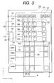
reference to FIG. 3. FIG. 3 is a block diagram for explaining a
relationship between a width of an internal circuit of the voltage
selector circuit 123 and a center-to-center spacing between two
adjacent ones of the video signal lines 103. The voltage selector
circuit 123 includes display data processing circuits 325 and
gray-scale voltage output circuits 326. Each of the display data
processing circuits 325 and the gray-scale voltage output circuits
326 is arranged on an extension line of a corresponding one of the
video signal lines 103.
Display data lines 321-323 from the display control device 111
(not shown) are connected to the horizontal drive circuit 120. Each
of the display data lines 321-323 corresponds to one bit of the display
data in digital form when the display data explained in connection
with FIGS. 1 and 2 are in digital representation. The display data
lines 321-323 represent respective ones of the display data line 132
indicated in FIGS. 1 and 2 corresponding one bit. The time control
signal lines 134 from the display control device 111 are connected
to the voltage selector circuit 123, but they are omitted in FIG. 3.
Display data are sequentially output to the display data lines
321-323, and the horizontal shift register 121 outputs timing signals
with which the display data are taken in synchronism. Timing signal
lines 329 from the horizontal shift register 121 are connected to the
voltage selector circuit 123, and they transmit timing signals to the
voltage selector circuit 123. Reference characters HSR1 to HSRn
denote bidirectional shift registers. The horizontal shift register
121 comprises the bidirectional shift registers HSR1 to HSRn. The
bidirectional shift registers HSR1 to HSRn output timing signals based
upon signals (shift clocks) from the timing control signal line 131.
Display data intended for each of the video signal lines 103
are output to the display data signal lines 321-323, and the display
data processing circuits 325 take in the display data in synchronism
with a corresponding one of the timing signals. The bidirectional
shift registers HSR0 and HSRn+1 are dummy.
In FIG. 3, the voltage generating circuit 112 is disposed on
one of the substrates forming the liquid crystal display panel 100,
and the gray-scale voltage line 133 from the voltage generating
circuit 112 is connected to the gray-scale voltage output circuit 326.
A number n of video signal lines 103 are arranged at approximately
equal intervals in the display section 110. A spacing between
adjacent ones of the video signal lines 103 is approximately equal
to the width of the pixel electrode 109 disposed in the display section
110. The number of the pixels to be provided in a given area of the
display section 110 is determined by the related standards. Therefore,
the area of the display section 110 and the number of the pixels
determine the size of the area where one pixel is fabricated. The
spacing between two adjacent ones of the video signal lines 103 is
selected based upon the size of the area where one pixel is formed.
For example, suppose that a number n of pixels are arranged in a
horizontal direction (in the X direction) in the display section 110
in FIG. 3, and the width of the display section 110 is W. Then the
pitch of the arrangement of the pixels is W/n, and the center-to-center
spacing between the video signal lines 103 is approximately
equal to the pixel pitch W/n. The widths of the display data
processing circuits 325 and the gray-scale voltage output circuits
326 arranged on the extension line of the video signal lines 103 are
approximately equal to the pixel pitch W/n.
On the extension line of each of the video signal lines 103
are provided the display data processing circuits 325 and the
gray-scale voltage output circuit 326 for outputting gray-scale
voltages to a corresponding one of the video signal lines 103.
Combinations of the display data processing circuits 325 and the
gray-scale voltage output circuit 326 are also disposed on two
extension lines adjacent to an arbitrary one of the extension lines
of the video signal lines 103. Therefore, if the widths of the display
data processing circuits 325 and the gray-scale voltage output
circuits 326 are not restricted within the horizontal pixel pitch,
a problem arises in that the display data processing circuits 325 or
the gray-scale voltage output circuits 326 overlap an adjacent one
of the display data processing circuits 325 and the gray-scale voltage
output circuits 326. Therefore, in a case where the area of the
display section is reduced, or the number of pixels is increased, a
problem arises in that consideration has to be given to the width of
the circuits so that the driving circuits can be formed within the
pixel pitch.
In the present embodiment, in order to arrange the display data
processing circuit 325 and the gray-scale voltage output circuit 326
efficiently within the horizontal pixel pitch, a plurality of the
display data processing circuits 325 are provided, each of which
corresponds to a corresponding one of the display data lines 321-323,
they are arranged in conformity with the arrangement of the
display data lines 321-323, and they are disposed on an extension line
of a corresponding one of the video signal lines 103.
As shown in FIG. 3, the display data lines 321-323 extend from
the display control device 111, and are connected to the display data
processing circuit 325. This embodiment explains a case where
three-bit display data representing eight gray-scale levels is used,
and the number of the display data lines 321-323 is three. In the
present embodiment, for simplicity, a case will be described where
the number of the display data lines is three, but it is possible to
select an arbitrary number of the display data lines depending upon
display data.
The display data processing circuits 325 are provided each of
which is associated with a corresponding one of the display data lines
321-323, performs digital processing using a corresponding bit of the
display signal, and then transmits a processing result to the
gray-scale voltage output circuit 326. The gray-scale voltage output
circuit 326 outputs a gray-scale voltage corresponding to the display
data based upon the processing results from the display data
processing circuit 325.
As described above, the spacing between the video signal lines
103 is limited by the size of the pixel electrodes 109 disposed in
the display section 110. On the other hand, the spacing between two
adjacent ones of the display lines 321-323 can be selected to wide
enough for each of the display data processing circuit 325 to be
disposed therebetween. As shown in FIG. 3, three display data
processing circuits 325 associated with one of the video display lines
103 are arranged in a line on the extension line of the one of the
video display lines 103 (in the Y direction in FIG. 3), and each of
the three display data processing circuits 325 is also arranged in
the vicinity of a corresponding one of the display data lines 321-323.
Consequently, the display data processing circuits 325 can be disposed
within the two adjacent ones of the video display lines 103.
However, the present inventors have found out that the spacing
between the display data lines cannot be made large freely, but it
is necessary to make the spacing as small as possible. Reduction of
the length as well as the width of the display data processing circuits
325 will be described subsequently.
The voltage selector circuit 123 will now be explained in
detail by reference to FIG. 4. FIG. 4 is a rough block diagram
illustrating a circuit configuration of the voltage selector circuit
123. In FIG. 4, only the configuration of the voltage selector circuit
123 associated with one of the video signal lines 103 are shown to
avoid complication of the figure.
As described above, the voltage selector circuit 123 is
provided with the display data processing circuits 325 each of which
is associated with a corresponding one of the display data lines
312-323. Each of the display data processing circuits 325 is
connected to a corresponding one of time control signal lines 161-163.
The time control signal lines 161-163 are included in the
control signal lines 134 indicated in FIGS. 1 and 2, and are connected
to the display control device 111 (not shown in FIG. 4).
In FIG. 4, reference numeral 122 denote display data hold
circuits, which store display data from the display data lines 321-323,
respectively, in synchronism with a signal supplied by the horizontal
shift register 121 via the timing signal line 329. Reference numerals
331, 332 and 333 denote processing-result transmitting circuits, each
of which performs digital processing by using outputs from the display
data hold circuits 122 and a signal from a corresponding one of the
time control signal lines 161-163, and outputs its processing result
to a processing-result signal line 152. The processing-result
transmitting circuits 331-333 are connected in series by the
processing-result signal line 152. The gray-scale voltage output
circuit 326 is also connected in series with the processing-result
transmitting circuits 331-333 by the processing-result signal lines
152. The gray-scale voltage output circuit 326 selects one of
gray-scale voltages on a voltage bus line 151 in accordance with a
processing result transmitted by the processing-result transmitting
circuits 331-333 and outputs it to the video signal line 103. The
voltage bus line 151 is the gray-scale line 133 indicated in FIGS.
1 to 3 in a case where a time-varying voltage is carried on the
gray-scale line. In FIG. 4, only one voltage bus line is provided,
but a plurality of voltage bus lines can be also utilized.
In the present embodiment, the processing-result transmitting
circuits 331-333 and the gray-scale voltage output circuit 326 are
connected by a smaller number of processing-result signal lines 152
than the number of the display data lines, and therefore a area
required for wiring can be reduced. To put it concretely, the data
transmitted by the three display data lines 321-323 are processed by
the three the processing-result transmitting circuits 331-333, then
their processing results are transferred in the vertical direction
via a single processing-result signal line 152, and therefore the
number of wirings is reduced. Further, the three processing-result
transmitting circuits 331-333 are arranged in the vertical direction,
and as a result the width of the circuit configuration for outputting
gray-scale voltages to the video signal line 103 can be reduced.
The following explains a method which selects a gray-scale
voltage and outputs to the video signal line 103 by using the
gray-scale voltage output circuit 326. The gray-scale voltage output
circuit 326 has the voltage bus line 151 connected thereto. A voltage
on the voltage bus line 151 varies periodically with time. When the
time-varying voltage on the voltage bus line 151 becomes a desired
voltage value, the gray-scale voltage output circuit 326 electrically
connects the voltage bus line 151 to the video signal line 103, but
when the time-varying voltage on the voltage bus line 151 is not equal
to the desired voltage value, the gray-scale voltage output circuit
326 disconnect the voltage bus line 151 from the video signal line
103, so that the desired voltage can be output as a gray-scale voltage
to the video signal line 103.
The following explains the operation of the voltage selector
circuit 123 briefly. Initially display data are stored in the display
data hold circuits 122 in synchronism with a timing signal output from
the horizontal shift register 121. Then the display data stored in
the display data hold circuits 122 are transmitted to the
processing-result transmitting circuits 331-333. Time control
signals on the time control signal lines 161-163 vary with time, and
the processing-result transmitting circuits 331-333 perform digital
processing by using the values from the display data hold circuits
122 and the values of the time control signals on the time control
signal lines 161-163. The processing results obtained by the
processing-result transmitting circuits 331-333 are transmitted to
the gray-scale voltage output circuit 326. When the voltage on the
voltage bus line 151 becomes equal to a gray-scale voltage represented
by the display data, the processing results obtained by the
processing-result transmitting circuits 331-333 are output and
thereby the gray-scale voltage output circuit 326 outputs the
gray-scale voltage from the voltage bus line 151, to the video signal
line 103.
Referring again to FIG. 4, the following explains a method in
which the processing-result transmitting circuits 331-333 are
composed of switching circuits, a voltage from a fixed-voltage line
153 is output to the processing-result signal line 152, and then is
transmitted to the gray-scale voltage output circuit 326 so that the
gray-scale voltage output circuit 326 can output a desired gray-scale
voltage.
Since the three processing-result transmitting circuits
331-333 are connected in series by the processing-
result signal line
152, the states represented by the processing-result transmitting
circuits 331-333 are the following two states only:
If the number of states transmitted to the gray-scale voltage
output circuit 326 is only two, it is difficult for the gray-scale
voltage output circuit 326 to output a plurality of gray-scale
voltages.
To solve this problem, in the present embodiment, the display
data processing circuits 325 are configured such that a certain number
of processing-result transmitting circuit are selected from a number
m (three in this embodiment) of the processing-result transmitting
circuits (331-333) so as to serve as switching circuits. With this
configuration, the number m of the processing-result transmitting
circuits (331-333) can represent a number 2m of states even if they
are connected in series by the processing-result signal line 152.
TABLE 1 shows variations of assignments of the three
processing-
result transmitting circuits 331, 332 and 333 for
switching circuits.
| Processing-result transmitting cicuits | Case | 1 | Case 2 | Case 3 | Case 4 | Case 5 | Case 6 | Case 7 | Case 8 |
| 333 | - | - | - | - | SW | SW | SW | SW |
| 332 | - | - | SW | SW | - | - | SW | SW |
| 331 | - | SW | - | SW | - | SW | - | SW |
In Table 1, "-" indicates that a processing-result transmitting
circuit is ON (conducting) at all times, and "SW" indicates that a
processing-result transmitting circuit serves as a switching circuit.
Although the three processing- result transmitting circuits 331, 332
and 333 are configured as switching circuits, if the processing-result
transmitting circuits are set to be ON at all times, the switching
circuits can be considered absent and conducting.
As described above, in a case where the switching
circuits are connected in series, only two states can be selected,
one is that all the switching circuits are ON, and the other one is
that at least one of the switching circuits is OFF. However, if, as
shown in TABLE 1, a number m (three in TABLE 1) of the switching circuits
(the processing-result transmitting circuits 331-333) are configured
such that, in each case, only a certain number of switching circuits
can be selected from the number m of the switching circuits for
switching operation, a number 2m of different states can be selected.
When a repetition period is divided into 2m intervals, and
different combinations of data time-varying with the period from a
plurality of the time control signal lines (161-163) at respective
ones of the 2m intervals is configured so as to represent a number
2m of different states, all of the processing-result transmitting
circuits (331-333) can be made conducting, and thereby the voltage
on the fixed-voltage line 153 can be transmitted to the gray-scale
voltage output circuit 326 during one of the 2m intervals corresponding
to display data, based upon the data from the time control signal lines
(161-163) and the display data.
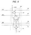
FIGS. 5 and 6 are circuit diagrams illustrating first and
second parts of a circuit configuration of the voltage selector
circuit 123 in the present embodiment, respectively, and a line end
designated A in FIG. 5 is connected to that designated A in FIG. 6.
In FIGS. 5 and 6 also, for simplicity, shown is a case in which display
data is composed of three bits. In FIG. 5, some of signal lines have
added references characters denoting signals transmitted thereto at
their left-hand ends and reference numerals assigned thereto at their
right-hand ends.
As shown in FIG. 5, each of the processing-result transmitting
circuits 331-333 in FIG. 4 is composed of two n-type transistors, one
of which serves as display data processing elements 201-203 and the
other of which serves as time data processing elements 211-213,
respectively.
Each of the display data processing circuits 325 of FIG. 4
includes data taking-in elements 171-173, memory capacitances 191-193,
and display data transfer elements 181-183, in addition to the display
data processing elements 201-203 and the time data processing elements
211-213, respectively. The display data processing circuits 325 are
connected to the display data lines 321-323 for supplying display data
DD1-DD3, to the time control signal lines 161-163 for supplying time
control signals DA1-DA3, and to transfer signal lines 167-169 for
supplying a transfer signal TG for controlling the display data
transfer elements 181-183, respectively.
The display data held in the memory capacitances 191-193 are
transferred to the display data processing elements 201-203 via the
display data transfer elements 181-183 in accordance with the transfer
signal TG. Reference numerals 153 and 156 denote fixed-voltage lines
for supplying a supply voltage VDD. Reference numeral 154 denotes
a fixed-voltage line for supplying a supply voltage GND. Reference
numeral 166 is the processing-result-signal-line set signal line, and
166 is a processing-result-signal-line reset signal line. In FIG.
6, reference numeral 141 denotes a level shift circuit, 142 is a gate
circuit, and 151 is the voltage bus line.
As shown in FIG. 5, when one of the display data processing
circuits 325 is provided for each of the display data lines 321-323,
and is composed of transistors of the same conductivity type only,
the length as well as the width of area occupied by the voltage selector
circuits 123 can be reduced in a liquid crystal display device.
First, before explaining the circuit of FIG. 5 in detail, the
size of an area required for fabricating elements of the circuits such
as the display data processing circuit 325 will be explained by
reference to FIGS. 7A, 7B, 8A-8C and 9A-9B.
FIGS. 7A and 7B are schematic cross-sectional views of
structures in which two transistors are fabricated side by side. FIGS.
7A and 7B illustrate conventional structures of general transistors.
FIG. 7A depicts a case in which two transistors of the same
conductivity type are fabricated side by side, and two n-type
transistors 230 are arranged side by side. FIG. 7B depicts a case
in which two transistors of opposite conductivity types are fabricated
side by side, on the left-hand side is an n-type transistor 230, and
on the right-hand side is a p-type transistor 240.
In FIG. 7A, reference numeral 232 denotes a p-type well, which
is fabricated in a semiconductor substrate 231 as by ion implantation,
n-type semiconductor layers 233 intended for source and drain regions
are fabricated in the p-type well 232 as by ion implantation.
Reference numeral 234 denotes a gate electrode, which is fabricated
on the p-type well 232 with a gate insulating film therebetween. The
two transistors 230 are isolated by a device-isolation region 235
fabricated as by LOCOS (Local Oxidation of Silicon). The device-isolation
regions 235 serve to electrically isolate elements from each
other in a case where a large number of elements are fabricated in
the same substrate, and each of the n-type transistors 230 is
fabricated in one of regions isolated from each other by the
device-isolation regions 235. In FIG. 7A, L1 represents a length of
the device-isolation region 235.
FIG. 7B illustrates a case where two transistors 230, 240 of
opposite conductivity types are fabricated side by side, reference
numeral 240 denotes a p-type transistor, 242 is an n-type well, 243
are p-type semiconductor layers, and 244 is a gate electrode. In this
case, a potential difference between adjacent elements becomes larger
compared with that in the case where the transistors of the same
conductivity type are fabricated side by side, and the p-type well
232 and the n-type well 242 are adjacent to each other, and therefore
a parasite transistor is easily formed, and consequently, it is
necessary to select the length L2 of a device-isolation region 245
to be larger than the length L1 of the device-isolation region 235.
As explained above, in a case where a plurality of transistors
are fabricated in the same substrate, if two transistors of opposite
conductivity types are arranged side by side, an area of a
device-isolation region increases and as a result a problem arises
in that a wasted area increases.
A relationship between the arrangement of transistors and an
area required for their fabrication will be explained by reference
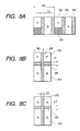
to FIGS. 8A-8C. FIGS. 8A, 8B and 8C illustrate three different cases,
each of which arranges two circuits composed of a pair of transistors.
FIG. 8A illustrates a case where two circuits are arranged in
a horizontal direction and each of the two circuits is composed of
a pair of transistors of opposite conductivity types (an n-type and
a p-type) and arranged in the horizontal direction. W1 in FIG. 8A
represents a with of an area required for each of the circuits. As
shown in FIG. 8A, the width W1 of the respective circuits includes
the width L2 of the device-isolation region 245. If an area of the
p-type well 232 is not equal to that of the n-type well 242, an unused
area 249 occurs.
FIG. 8B illustrates a case where two circuits of the same
configuration are arranged in a horizontal direction, and each of the
two circuits is composed of a pair of transistors of opposite
conductivity types (an n-type and a p-type) and arranged in a vertical
direction. The width of an area occupied by each of the two circuits
is W2. The width W2 is smaller than the width W1, and therefore this
configuration is effective for disposing the circuits within the pixel
pitch as explained above. However, a device-isolation region 245
having a length L2 is disposed between the p-type and n-type wells
arranged in a vertical direction, and therefore the length of the
configuration of FIG. 8B is longer compared with that of a
configuration in which two transistors of the same conductivity type
are arranged in the vertical direction.
FIG. 8C illustrates a case where two circuits of the same
configuration are arranged in a horizontal direction, and each of the
two circuits is composed of a pair of transistors of the same
conductivity type and arranged in a vertical direction. The length
of a device-isolation region 235 is L1, which is smaller than the
length L2 of FIG. 8B. Although a difference between the lengths L1
and L2 is of the order of several µm at the most, if a plurality of
circuits each of which is composed of a pair of transistors are
arranged successively in the vertical direction, the differences are
cumulative, i.e., they add up, and therefore they cannot be ignored.
When the circuits are employed in the display data processing circuit
325 of FIG. 3, for example, one display data is represented in three
bits, and therefore the cumulative difference is three times the
difference between the lengths L1 and L2. As the number of gray-scale
levels displayed on a liquid crystal display panel is increased,
and therefore as the number of bits for representing display data is
increased to 8, or 16, it is effective to reduce the area of useless
regions by improving the arrangement of the transistors.
In the present embodiment, as shown in FIG. 5, the data
taking-in elements 171-173, the display data transfer elements
181-183, display data processing elements 201-203, and the time data
processing elements 211-213 are formed of transistors of the same
conductivity type, and consequently, the areas of the device-isolation
regions required for the side-by-side arrangement of the
transistors are further reduced. In FIG. 5, the n-type transistors
are employed, but it is needless to say that this embodiment can be
realized by using p-type transistors for the side-by-side arrangement
of transistors of the same conductivity type, instead of the n-type
transistors.
FIGS. 9A and 9B illustrates the layout of the display data
processing element 203 and the time data processing element 213, FIG.
9A is a schematic plan view illustrating the layout, and FIG. 9B is
a schematic cross-sectional view taken along line IXB-IXB of FIG. 9A.
In FIG. 9A, the device-isolation region 235 is fabricated by the LOCOS
process, and covers the semiconductor substrate 231 serving as a field
oxide film. Reference numeral 236 denotes an active region disposed
in the device-isolation region (the field oxide film) 235. In the
active region 236 are the display data processing element 203 formed
of a transistor and the time data processing element 213 formed of
a transistor. Reference numeral 234 denote gate electrodes. To
simplify FIGS. 9A and 9B, wiring is omitted in FIG. 9A, and electrical
connections in FIG. 9B are represented by lines.
As indicated in FIG. 5, the display data processing element
203 and the time data processing element 213 are connected to the
processing-result signal line 152, and since the display data
processing elements 201-203 and the time data processing elements
211-213 can be fabricated in the same substrate and they can share
common source or drain regions, their source or drain regions are
coupled together so as to be at the same potentials. As shown in FIG.
9B, a source or drain region 233A is configured so as to be shared
by the display data processing element 203 and the time data processing
element 213, and therefore a multilayer wiring between the source or
drain regions of the two elements 203 and 213. Because each of pairs
of the display data processing elements 201-203 and the time data
processing elements 211-213 shares the source or drain region 233A,
it is not necessary to fabricate the device-isolation regions 235
between the display data processing elements 201-203 and the time data
processing elements 211-213.
As shown in FIGS. 9A and 9B, the processing-result transmitting
circuits 331-333 are composed of the two transistors, one for the
display data processing element 203 and one for the time data
processing element 213, the need for the device-isolation region 235
and an area for wiring can be eliminated by using the two transistors
of the same conductivity type, and as a result, the area occupied by
the two transistors has been made smaller than that occupied by two
transistors of opposite conductivity types and arranged side by side.
Consequently, the display data processing circuit 325 can be formed
into a compact structure. A multilayer wiring between the display
data processing elements 201-203 and the time data processing elements
211-213 are omitted, thereby reducing capacitances due to wiring and
making possible high-speed operation.
As shown in FIGS. 5, 9A and 9B, in the processing-result
transmitting circuits 331-333, each of the display data processing
elements 201-203 is formed of one transistor, and each of the time
data processing elements 211-213 is also formed of one transistor.
Since the processing-result transmitting circuits 331-333 perform a
digital processing by using display data and time control signals,
they need an element for display data and an element for time control
signals, and therefore each of the processing-result transmitting
circuits 331-333 needs at least two elements. Therefore, each of the
processing-result transmitting circuits 331-333 shown in FIG. 5 is
formed of the smallest number of elements. As described above, the
area occupied by each of the processing-result transmitting circuits
331-333 can be made smaller than that occupied by a processing-result
transmitting circuit fabricated by using the smallest number, two,
of conventional transistors.
FIG. 10 illustrates a layout of the display data processing
circuit 325. To simplify FIG. 10, wiring conductors other than the
timing signal line 329 are omitted, and they are represented by lines.
As explained in connection with FIGS. 9A and 9B, the display data
processing element 203 and the time data processing element 213 are
transistors forming the processing-result transmitting circuit 333.
The data taking-in element 173 and the display data transfer element
183 shares a source or drain region equal in potential to one of two
electrodes forming the memory capacitance 193. Consequently, the
data taking-in element 173 and the display data transfer element 183
can be fabricated in the same substrate, and a device-isolation region
between them and wiring region can be omitted.
As shown in FIG. 10, the timing signal line 329 is formed of
the same conductive layer as the gate electrode of the data taking-in
element 173. The timing signal line 329 is disposed adjacently to
the processing-result transmitting circuit 333 and the memory
capacitance 193, and a portion of the timing signal line 329 is used
as a gate electrode of the data taking-in element 173.
An active region 271 for the data taking-in element 173 and
the display data transfer element 183 is patterned such that its
portions overlapped by the gate electrodes of the elements 173 and
183 are trapezoids. These shapes cause preferred directions in which
charges appearing below the gate electrodes move easily. When the
transistor is in an ON state with a voltage applied on the gate
electrode, charges are generated in the active region below the gate
electrode, and then when the transistor is changed into an OFF state,
the charges flow into one of its source and drain regions. When a
difference in length is present between the two opposing long sides
of a portion of one gate electrode overlapping with the active region
271 as shown in FIG. 10, the charges flow easily toward the longer
one of the two long sides.
In the case of the data taking-in element 173, when a signal
of positive polarity is intended to be taken into the memory
capacitance 193, the amount of negative charges flowing from the
memory capacitance 193 into the display data signal line 323 is very
small. Therefore, when the transistor (the data taking-in element
173) is turned OFF, if the charges below its gate electrode have flowed
into the memory capacitance 193, a sufficient signal cannot be written
into the memory capacitance 193. To eliminate this problem, the
active region 271 is shaped as shown in FIG. 10 so that the charges
can flow into the display data signal line 323 easily. The display
data transfer element 183 also produces the same advantages such that
the signal can be transferred easily to the succeeding circuit.
The following explains the operation of the circuit shown in
FIGS. 5 and 6 by reference to timing charts of the signals shown in
FIGS. 11 and 12.
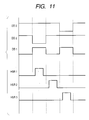
FIG. 11 illustrates the display data DD1-DD3 output to the
display data lines 321-323, respectively, and the timing signals
HSR1-HSR3 output from the horizontal shift register 121. In FIG. 5,
the display data DD1-DD3 are output to the display data lines 321-323,
respectively, and the horizontal shift register 121 outputs the timing
signals HSR1-HSR3 sequentially. In FIG. 11, only three timing signals
HSR1-HSR3 are shown, but it is to be understood that a necessary number
of the timing signals are output from the horizontal shift register
in accordance with the number of the video signal lines.
The display data DD1-DD3 represent three-bit data with DD1
being assigned to the lowest-order bit. During the time when the
timing signal HSR1 is output, the display data DD1 is at a high level,
the display data DD2 is at a low level, and the display data DD3 is
at the high level. In the display data DD1-DD3 of this embodiment,
the high and low levels are represented by "1" and "0", respectively,
and therefore the above display data during the time when the timing
signal HSR1 is output is represented as (1, 0, 1) in the order from
the lowest-order bit.
In FIG. 11, in a state in which the display data DD1-DD3 are
(1, 0, 1), when the timing signal HSR1 is output to the timing signal
line 329, the data taking-in elements 171-173 are turned ON, and
thereby the display data DD1-DD3 are taken into the memory
capacitances 191-193, respectively. When the display data DD1-DD3
are (1, 0, 1), the memory capacitance 191 takes in a high-level voltage,
the memory capacitance 192 takes in a low-level voltage, and the memory
capacitance 193 takes in the high-level voltage.
Operation after the display data have been taken into the
memory capacitances 191-193 will be explained by reference to FIG.
12. In FIG. 12, reference character RMP denotes a gray-scale voltage,
which is supplied to the bus line 151 shown in FIG. 6 from the voltage
generating circuit 112 (not shown). The gray-scale voltage RMP varies
with time in the staircase fashion as shown in FIG. 12, where the
assignment is made that when the display data are (1, 1, 1), a
gray-scale voltage V0 is written into a pixel electrode, and when the
display data are (0, 0, 0), a gray-scale voltage V7 is written into
a pixel electrode.
In FIG. 12, first when the transfer signal TG changes to the
high level, the display data transfer elements 181-183 are turned ON,
and thereby the display data held in the memory capacitances 191-193
are transferred to the display data processing elements 201-203.
Although potentials corresponding to with the display data are
transferred to the gate electrodes of the display data processing
elements 201-203, respectively, because the charges which were
present a horizontal scanning period earlier are stored in the gate
electrodes of the display data processing elements 201-203, the
potentials of the gate electrodes are determined by voltage division
based upon the memory capacitances 191-193 and capacitances of the
respective gate electrodes and their wiring, of the potentials stored
in the respective memory capacitances 191-193 and the potentials which
were present in the respective gate electrodes a horizontal scanning
period earlier. When the display data DD1-DD3 are (1, 0, 1) as shown
in FIG. 11, the display data processing elements 201 and 203 are turned
ON, and the display data processing element 202 are turned OFF.
Next in a state in which the time control pulses DA1-DA3 are
at the high level, the processing-result-signal-line set signal DST
is set to the low level so that a processing-result-signal-line set
element 222 is turned OFF. Then the processing-result-signal-line
reset signal DRST is set to the low level so that two processing-result-signal-line
set elements 221 and 223 is turned OFF, and as a
result the processing-result signal lines 152(1) and 152(4) are
connected to the fixed- voltage lines 153 and 156, respectively, and
changes to the high level.
When the processing-result signal line 152 is at the high level,
the level shift circuit 141 of the gray-scale voltage output circuit
326 supplies gate voltages to the gate circuit 142 so that the gate
circuit 142 electrically connects the voltage bus line 151 to the video
signal line 103. This means that, during the time when the
processing-result signal line 152 is at the high level, the video
signal line 103 is supplied with the gray-scale voltage RMP from the
voltage bus line 151. As explained above, the gray-scale voltage RMP
in FIG. 12 varies with time in the staircase fashion. During the time
when the processing-result signal line 152 is at the high level, the
gray-scale voltage RMP shown in FIG. 12 is output to the video signal
line 103.
Next the time control pulses DA1-DA3 start to be output to the
time control signal lines 161-163, respectively. Then the
processing-result-signal-line reset signal DRST is set to the high
level, and then the processing-result-signal-line set signal DST is
set to the high level. When the processing-result-signal-line set
signal DST changes to the high level, the processing-result-signal-line
set element 222 is turned ON, the processing-result signal
line 152(1) is connected to the line 154 at the GND level, and changes
to the low level.
In FIG. 12, at time t0, all of the time control pulses DA1-DA2
are at the low level, and therefore all of the time data processing
elements 211-213 are ON. As a result, unless all of the display data
processing elements 201-203 are ON, i.e., unless the display data
201-203 are (1, 1, 1), the potential of the processing-result signal
line 152(4) is kept at the voltage VDD, and thereby the gate circuit
142 remains on the ON state.
In FIGS. 5, 6, 11 and 12, consider the display data are (1,
0, 1) in the time when the timing signal HSR1 is output, for example.
At time t0, the display data processing element 202 is turned
OFF, and the processing-result signal line 152 (4) is kept at VDD.
After that, at time t2 the time control pulses DA1-DA3 become
(0, 1, 0), and thereby the time data processing element 212 is turned
ON. On the other hand, since the display data are (1, 0, 1), the
display data processing elements 201 and 203 are in the ON state.
Consequently, all of the processing-result signal line 152(1) to
152(4) are connected the GND line 154, the processing-result signal
line 152(4) changes to the low level, and therefore the gate circuit
142 electrically disconnects the voltage bus line 151 from the video
signal line 103. Consequently, the video signal line 103 is held at
a voltage V2 present on the voltage bus line 151 at the instant when
the video signal line 103 is disconnected from the voltage bus line
151. Thereafter the video signal line 103 is not electrically
connected to the voltage bus line 151 until the processing-result-signal-line
reset signal DRST changes to the low level and
thereby the processing-result signal line 152 is set to the high level.
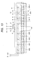
The circuit configuration of the horizontal shift register 121
will be explained by reference to FIG. 13. Reference character HSR
denotes a bidirectional shift register which can shift a signal
leftward and rightward. The bidirectional shift register HSR is
composed of clocked inverters 61, 62, 65 and 66.
Reference numeral 25 is an input terminal for a horizontal
scanning reset signal, and 26 is an input terminal for a horizontal
scanning start signal. The clocked inverters 61 provide the start
signal to the horizontal shift register 121 for scanning in the
left-to-right direction in FIG. 13, and the clocked inverters 62
provide the start signal to the horizontal shift register 121 for
scanning in the right-to-left direction in FIG. 13. Reference numeral
27 denotes an output terminal for a signal for completing the
horizontal scanning.
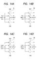
The clocked inverters 61 and 62 employed in the bidirectional
shift registers HSR will be explained by reference to FIGS. 14A and
14B. Reference characters RL1 and RL2 denote first and second
horizontal direction-setting lines, respectively. The first
horizontal direction-setting line RL1 provides an H level for scanning
in the left-to-right direction in FIG. 13, and the second horizontal
direction-setting line RL2 provides an H level for scanning in the
right-to-left direction in FIG. 13. For clarity, wiring is omitted
in FIG. 13, but the first and second horizontal direction-setting
lines RL1 and RL2 are connected to the clocked inverters 61 and 62
constituting the bidirectional shift register HSR.
The clocked inverter 61 is composed of p- type transistors 71,
72 and n- type transistors 73, 74 as shown in FIG. 14A. The p-type
transistor 72 is connected to the second horizontal direction-setting
line RL2, and the n-type transistor 73 is connected to the first
horizontal direction-setting line RL1. When the first horizontal
direction-setting line RL1 is at the H level and the second horizontal
direction-setting line RL2 is at the L level, the clocked inverter
61 serves as an inverter, but when the first horizontal
direction-setting line RL1 is at the L level and the second horizontal
direction-setting line RL2 is at the H level, the clocked inverter
61 serves as a high impedance.
On the other hand, in the clocked inverter 62, the p-type
transistor 72 is connected to the first horizontal direction-setting
line RL1, and the n-type transistor 73 is connected to the second
horizontal direction-setting line RL2. When the second horizontal
direction-setting line RL2 is at the H level, the clocked inverter
62 serves as an inverter, and when the first horizontal
direction-setting line RL1 is at the H level, the clocked inverter
62 serves a high impedance.
FIG. 14C illustrates a circuit configuration of the clocked
inverter 65. When a clock signal line CLK1 is at the H level, and
a clock line signal CLK2 is at the L level, the clocked inverter 65
outputs an inverted input, and when the clock signal line CLK1 is at
the L level, and the clock signal line CLK2 is at the H level, the
clocked inverter 65 serves as a high impedance.
FIG. 14D illustrates a circuit configuration of the clocked
inverter 66. When the clock signal line CLK1 is at the L level, and
the clock signal line CLK2 is at the H level, the clocked inverter
66 outputs an inverted input, and when the clock signal line CLK1 is
at the H level, and the clock signal line CLK2 is at the L level, the
clocked 66 inverter serves as a high impedance. For clarity,
connections of the clock signal lines CLK1, CLK2 are omitted in FIG. 13,
but the clock signal lines CLK1 and CLK2 are connected to the clocked
inverters 65 and 66.
FIGS. 15A and 15B illustrate a layout of transistors
constituting the horizontal drive circuit 120. FIG. 15A is a
schematic plan view of the horizontal drive circuit 120, and for
clarity, the horizontal drive circuits 120 corresponding to only four
of the video signal lines 103 (not shown) are shown in FIGS. 15A and
15B. The width AW of each of the horizontal drive circuits 120
corresponding to a respective one of the video signal lines 103 is
determined by the pixel pitch as explained above. FIG. 15B is a
schematic cross-sectional view of the horizontal drive circuits 120
taken along line XVB-XVB of FIG. 15A.
Reference numeral 121 denotes the horizontal shift register,
which is composed of n-type transistors and p-type transistors
arranged side by side as shown in FIGS. 14A-14D. Reference numerals
246 and 236 denote active regions of the p-type and n-type transistors,
respectively. In the active region 246(1), for example, the p-type
transistors of the clocked inverters 61 and 62 of FIGS. 13, 14A and
14B are arranged side by side within the width AW. Likewise, in the
active region 236(1) are fabricated the n-type transistors of the
clocked inverters 61 and 62, in the active region 246(2) are fabricated
the p-type transistors of the clocked inverters 65 and 66, and in the
active region 236(2) are fabricated the n-type transistors of the
clocked inverters 65 and 66. In FIG. 15B, reference numeral 242 denote
n-type wells, 232 are p-type wells, and 245 are device-isolation
regions provided between the n-type and p-type wells. Reference
character AL2 denotes the length of the area where the horizontal shift
registers 121 are formed. Reference numeral 325 denotes the display
data processing circuit 325. In FIGS. 15A and 15B, six of the display
data processing circuits 325(1)-325(6) are arranged in the vertical
direction. Each of the display data processing circuit 325(1)-325(6)
is provided so as to correspond to a respective one of the video signal
lines 103, and therefore as the number of bits of the display data
is increased, the area where the display data processing circuits are
formed has to be lengthened in the vertical direction. To solve this
problem, the display data processing circuit 325 is composed of the
n-type transistors as shown in FIG. 5.
Reference numeral 236 in FIGS. 15A and 15B denote the active
regions where the display data processing elements (designated
201-203 in FIG. 5) and the time data processing elements (designated
211-213 in FIG. 5) of FIG. 5. The display data processing element
203 and the time data processing element 213 are arranged laterally
in the active region 236 as shown in FIGS. 9A and 9B. In FIG. 15B,
reference numeral 232 denotes the n-type well, and 235 is the
device-isolation region provided between the two n-type wells.
Reference character AL1 denotes the length of the area where each of
the display data processing circuits 325(1)-325(6) is formed. In FIGS.
15A and 15B, reference numeral 261 denote regions where the memory
capacitances 191-193 of FIG. 5 are formed, and 261 are active regions
where the data taking-in elements of FIG. 5 (designated 171-173 in
FIG. 5) and the display data transfer elements of FIG. 5 (designated
181-183 in FIG. 5) are formed. The data taking-in elements and the
display data transfer elements are laterally arranged in the active
region 271 like the display data processing elements and the time data
processing elements.
Reference numeral 329 in FIG. 15A denote timing signal lines
(made of poly-silicon, for example) extending from the horizontal
shift register 121 and connected to the respective ones of the data
taking-in elements (wiring to the data taking-in elements are omitted
in FIGS. 15A and 15B). Each of the timing signal lines 329 are disposed
along the display data processing circuits 325(1)-325(6) so that it
can supply the timing signal to all of the display data processing
circuit 325(1)-325(6). Therefore the timing signal lines 329 are
lengthened in the vertical direction as the number of bits of the
display data is increased, and hence the number of the display data
processing circuits 325(1), 325(2),... is increased.
As the timing signal line 329 is lengthened, wiring resistance
increases. Since the timing signal is a pulse of high frequency, the
increase in the wiring resistance causes distortions in the waveform
of the timing signal. The waveform distortions in the timing signal
produces errors in timing of taking-in of the display data into the
data taking-in elements 171-173. For example, a problem arises in
that, while the display data processing circuit 325(1) has taken in
a display data at a given instant of time, the display data processing
circuit 325(6) has not taken in a display data, and display quality
is degraded.
When the wiring resistance and capacitance of the timing signal
line 329 are considered, it is desirable to make the length AL1 of
the display data processing circuit 325 as short as possible. When
the length AL2 of the horizontal shift register 121 is longer than
the length AL1 of each of the display data processing circuits 325(1),
325(2), 325(3),.... The overall length of the display data processing
circuits 325(1), 325(2), 325(3),... is the product of the length AL1
and the number of the display data bit, and therefore, if the number
of display data bits is increased, it is effective for reducing the
lengths of the entire circuits and the timing signal lines 329 to
shorten the length AL1 of each of the display data processing circuits
325(1), 325(2), 325(3),..... In view of the above, the length AL1
of the display data processing circuits 325(1), 325(2), 325(3),....
is reduced by forming the circuits 325(1), 325(2), 325(3),.... using
n-type transistors, and thereby reducing the length of the
device-isolation regions 235.
In FIG. 15A, reference numeral 326 denotes the gray-scale
voltage output circuit, 272 and 273 are active regions of p-type and
n-type transistors of the level shift circuit 141, respectively. The
active region 273 are made larger than the other active regions for
increasing the ON and OFF speeds of the transistors.
As explained above, in the design of the layout of transistors
constituting the horizontal drive circuit 120, the length of the drive
circuit can be reduced by forming the drive circuit by using
transistors of the same conductivity type and locating the circuit
within the pixel pitch. Even if the area of the display section of
a liquid crystal display panel is reduced, but the numbers of
gray-scale levels and pixels are increased, the drive circuit can be
realized which has an area smaller than the display section. The
wiring resistance of the timing signal lines used for taking in display
data can be kept to a low value by shortening the length of the drive
circuit even when the number of gray scale levels, and thereby errors
in taking-in the display data can be reduced.
FIG. 16 illustrates a configuration employing two systems of
the horizontal drive circuits 120. In FIG. 16, the two systems of
the horizontal drive circuits 120 are illustrated as disposed at the
top and bottom sides of the display section 110, but both of the two
systems can be disposed at one of the top and bottom sides of the display
section 110. FIG. 17 illustrates a circuit configuration of the
voltage selector circuit 123 suitable for a case in which two systems
of the horizontal drive circuits 120 are employed. In the horizontal
drive circuits 120 shown in FIG. 16, during the time when the voltage
selector circuit 123 in one of the two systems takes in display data,
the voltage selector circuit 123 in the other of the two systems can
select a gray-scale voltage, and as a result the display data transfer
elements can be omitted as shown in FIG. 17.
The following explains the pixel section in the liquid crystal
display device in accordance with the present invention by reference
to FIG. 18. FIG. 18 is a schematic cross-sectional view of an
embodiment in accordance with the present invention.
In FIG. 18, reference numeral 100 denotes a liquid crystal
display panel, 1 is a first substrate serving as a drive circuit
substrate, 2 is a second substrate serving as a transparent substrate,
3 is a liquid crystal composition, 4 are spacers. The spacers 4
establish a fixed cell gap d between the drive circuit substrate 1
and the transparent substrate 2 which sandwich the liquid crystal
composition 3. Reference numeral 5 denotes a reflective electrode
formed on the drive circuit substrate 1, 6 is a counter electrode for
applying a voltage across the liquid crystal composition 3 in
cooperation with the reflective electrode 5, 7 and 8 are orientation
films for orientating liquid crystal molecules of the liquid crystal
composition 3 in specified directions, and 30 are active elements for
applying a voltage to the reflective electrode 5.
Reference numeral 34 denote drain regions, 35 are source
regions, 36 are gate electrodes, 38 are insulating films, 39 are field
oxide films for electrically isolating transistors from each other,
40 is a storage-capacitance-forming electrode for forming a
capacitance in cooperation with the drive circuit substrate 1 with
an insulating film 38 interposed therebetween, 41 are first interlayer
insulating films, 42 are first conductive films, 43 are second
interlayer insulating films, 44 are first light blocking films, 45
are third interlayer insulating films, 46 are second light blocking
films, 47 are fourth interlayer insulating films, and 48 are second
conductive films forming the reflective electrodes 5.
The liquid crystal display panel in this embodiment is of the
reflective type. Light projected into the liquid crystal display
panel 100 enters from the transparent substrate 2 (at the top of FIG.
18), then passes through the liquid crystal composition 3, then is
reflected back by the reflective electrode 5, then passes through the
liquid crystal composition 3 and the transparent substrate 2 again,
and then leaves the liquid crystal display panel 100.
In the liquid crystal display panel of the reflective type,
when the reflective electrode 5 is disposed on the surface of the drive
circuit substrate 1 on its liquid crystal composition 3 side, an opaque
substrate such as a silicon substrate can be used as the drive circuit
substrate 1. This structure has advantages that the active elements
30 and wiring can be disposed below the reflective electrodes 5,
thereby the area of the reflective electrodes 5 can be increased which
form pixels, and consequently, the higher aperture ratio can be
realized. Also this structure has an advantage of radiating heat
generated by light projected into the liquid crystal display panel
100 from the back surface of the drive circuit substrate 1.
Next, operation of the liquid crystal display panel employing
the electrically controlled birefringence mode will be explained.
Light linearly polarized by a polarizer enters the liquid crystal
display panel 100. When a voltage is applied between the reflective
electrode 5 and the counter electrode 6, orientation of liquid crystal
molecules of the liquid crystal composition 3 is changed due to their
dielectric anisotropy, and as a result the birefringence of the layer
of the liquid crystal composition 3 is changed. The electrically
controlled birefringence mode generates images by converting the
changes of the birefringence into the changes of light transmission.
Next, the single-polarizer twisted nematic (SPTN) mode, which
is one type of the electrically controlled birefringence mode, will
be explained by reference to FIGS. 19A and 19B.
Reference numeral 9 denotes a polarizing beam
splitter which divides an incident light L1 from a light
source (not shown) into two polarized lights, and a
linearly polarized light L2 of the two is emitted.
In FIGS. 19A and 19B, a light having passed through
the polarizing beam splitter 9, which is a p-polarized
light, is entered into the liquid crystal display panel
100, but instead a light reflected by the polarizing beam
splitter 9, which is an s-polarized light, can be entered
into the liquid crystal display panel 100.
The liquid crystal composition 3 is a nematic liquid
crystal material having positive dielectric anisotropy.
Longitudinal axes of the liquid crystal molecules are
oriented approximately in parallel with the major
surfaces of the drive circuit substrate 1 and the
transparent substrate 2, and the liquid crystal molecules
are twisted through about 90 degrees across the liquid
crystal layer by the orientation films 7, 8.
FIG. 19A illustrates a case where no voltage is
applied across the layer of the liquid crystal composition
3. The light L2 entering the liquid crystal display panel
100 is converted into elliptically polarized light by
birefringence of the liquid crystal composition 3, and
then becomes circularly polarized light on the reflective
electrode 5. The light reflected by the reflective
electrode 5 passes through the liquid crystal composition
3 again, thereby becomes elliptically polarized light
again, and then returns to linearly polarized light again
when it leaves the liquid crystal display panel 100. The
emergent linearly polarized light L3 is s-polarized light
having its direction of polarization rotated through an
angle of 90° with respect to that of the incident light
L2, enters the polarizing beam splitter 9 again, and then
is reflected by an internal interface of the polarizing
beam splitter 9 to become emergent light L4 which in turn
is projected onto a screen or the like to produce a display.
This configuration is of the so-called normally white
(normally open) type which emits light when a voltage is
not applied across the layer of the liquid crystal
composition 3.
FIG. 19B illustrates a case where a voltage is
applied across the layer of the liquid crystal composition
3. When an electric field is applied across the layer
of the liquid crystal composition 3, the liquid crystal
molecules align in a direction of the electric field and
consequently, the birefringence of the liquid crystal
molecules does not appear. As a result, the linearly
polarized light L2 entering the liquid crystal display
panel 100 is reflected by the reflective electrode 5
without undergoing changes, and then the light L5 emergent
from the liquid crystal display panel 100 has the same
direction of polarization as that of the incident light
L2. The emergent light L5 passes through the polarizing
beam splitter 9, and returns to the light source such that
no light is projected onto the screen and a black display
is provided on the screen.
In the single-polarizer twisted nematic mode, the
direction of orientation of the liquid crystal molecules
is parallel with the major surfaces of the substrates,
and therefore usual methods of orientating the liquid
crystal molecules can be employed and its manufacturing
process is highly stable. The normally white mode
operation is preventive of defective displays occurring
at low voltage levels . The reason is that, in the normally
white mode, a dark level (a black display) is provided
when a high voltage is applied across the liquid crystal
layer, and in this state, almost all the liquid crystal
molecules are orientated in the direction of the electric
field which is perpendicular to the major surfaces of the
substrates, and consequently, a display of the dark level
does not depend very much upon the initial conditions of
orientation of the liquid crystal molecules having a low
electric field applied thereto.
The human eye perceives non-uniformity in luminance
based upon the ratio of luminances, is responsive
approximately to the logarithm of luminance, and
consequently, is sensitive to variations in dark levels.
Because of the above reasons, the normally white
mode has advantages with respect to prevention of
non-uniformity in luminance caused by initial conditions
of orientation of the liquid crystal molecules.
The electrically controlled birefringence mode requires a
highly precise cell gap between the substrates of the liquid crystal
display panel. The electrically controlled birefringence mode
utilizes a phase difference between ordinary rays and extraordinary
rays caused while they pass through the liquid crystal layer, and
therefore the intensity of the light transmission through the liquid
crystal layer depends upon the retardation Δ n · d between the ordinary
and extraordinary rays, where Δ n is a birefringence and d is a cell
gap established by spacers 4 between the transparent substrate 2 and
the drive circuit substrate 1.
In this embodiment, in view of non-uniformity in display, the
cell gap was controlled with accuracy of ± 0.05 µm. In the
reflective type liquid crystal display panel, light entering the
liquid crystal layer is reflected by the reflective electrode, and
then passes through the liquid crystal layer again, therefore, if the
reflective type liquid crystal display panel uses a liquid crystal
composition having the same birefringence Δ n as that of a liquid
crystal composition used in the transmissive type liquid crystal
display panel, the cell gap d of the reflective type liquid crystal
display panel is half that of the transmissive type liquid crystal
display panel. Generally, the cell gap d of the transmissive liquid
crystal display panel is in a range of from about 5 microns to about
6 microns, but in this embodiment the cell gap d is selected to be
about 2 microns.
In this embodiment, to ensure a high accuracy of the cell gap
and a smaller cell gap than that of conventional liquid crystal display
panels, column-like spacers are fabricated on the drive circuit
substrate 1 instead of using a bead-dispersing method.
FIG. 20 is a schematic plan view of a liquid crystal
display panel for explaining an arrangement of the
reflective electrodes 5 and the spacers 4 disposed on the
drive circuit substrate 1. A large number of spacers 4
are arranged in a matrix array over the entire area of
the drive circuit substrate 1 for establishing a uniform
spacing between the transparent substrate 2 and the drive
circuit substrate 1. Each of the reflective electrodes
5 defines a pixel serving as the smallest picture element
formed by the liquid crystal display panel. For the sake
of simplicity, FIG. 20 illustrates an array of five columns
by four rows of pixels, pixels in the outermost columns
and rows are represented by reference numeral 5B, pixels
within the outermost columns and rows are represented by
reference numeral 5A.
In FIG. 20, the array of five columns by four rows
of pixels forms a display area, in which a display by the
liquid crystal display panel is formed. Dummy pixels 10
are disposed around the display area, a peripheral frame
11 made of the same material as that of the spacers 4 is
disposed around the dummy pixels 10, and a sealing member
12 is coated around the peripheral frame 11 on the drive
circuit substrate 1. Reference numeral 13 denotes
terminals for external connections which are used for
supplying external signals to the liquid crystal display
panel 100.
The spacers 4 and the peripheral frame 11 are formed
of resin material. As the resin material can be used a
chemically amplified type negative photoresist "BPR-113"
(a trade name) manufactured by JSR Corp. (Tokyo, Japan),
for example. The photoresist material is coated as by
a spin coating method on the drive circuit substrate 1
having the reflective electrodes 5 formed thereon, then
is exposed through a mask having a pattern in the form
of the spacers 4 and the peripheral frame 11, and then
is developed by a remover to form the spacers 4 and the
peripheral frame 11.
When the spacers 4 and the peripheral frame 11 is
fabricated by using photoresist or the like as their
material, the height of the spacers 4 and the peripheral
frame 11 can be controlled by coating thickness of the
material, and therefore the spacers 4 and the peripheral
frame 11 can be fabricated with high precision. The
positions of the spacers 4 can be determined by the mask
pattern, and consequently, the spacers 4 can be located
at the desired positions accurately.
In the liquid crystal display panel employed in a
liquid crystal projector, if one of the spacers 4 is
present on a pixel, a problem arises in that a shadow of
the spacer 4 is visible in its projected enlarged image.
By fabricating the spacers 4 by exposure through a mask
pattern and subsequent development, the spacers 4 can be
located at such positions as not to deteriorate the quality
of a displayed image.
Since the spacers 4 and the peripheral frame 11 have
been fabricated simultaneously, the liquid crystal
composition 3 can be sealed between the drive circuit
substrate 1 and the transparent substrate 2, by initially
dropping a small amount of the liquid crystal composition
3 on the drive circuit substrate 1, then overlapping the
transparent substrate 2 on the drive circuit substrate
1 with the liquid crystal layer therebetween, and then
bonding the transparent substrate 2 to the drive circuit
substrate 1.
When the liquid crystal display panel 100 has been
assembled after interposing the liquid crystal
composition 3 between the driving circuit substrate 1 and
the transparent substrate 2, the liquid crystal
composition 3 is held within a region surrounded by the
peripheral frame 11.
The sealing member 12 is coated around the outside
of the peripheral frame 11 and confines the liquid crystal
material 3 within the liquid crystal display panel 100.
As described above, the peripheral frame 11 is
fabricated by using the pattern mask, and therefore it
is fabricated on the driving circuit substrate 1 with high
positional accuracy, and consequently, the border of the
liquid crystal composition 3 can be defined with high
accuracy. Further, the peripheral frame 11 can define
the border of the sealing member 12 with high accuracy.
The sealing member 12 serves to fix the driving
circuit substrate 1 and the transparent substrate 2
together, and also serves to prevent materials harmful
to the liquid crystal composition 3 from penetrating
thereinto. When the fluid sealing member 12 is applied,
the peripheral frame 11 serves as a stopper against the
sealing member 12. By disposing the peripheral frame 11
as the stopper against the sealing member 12, the borders
of the liquid crystal composition 3 and the sealing member
12 can be established with high precision, and
consequently, the region between the display area and the
peripheral sides of the liquid crystal display panel 100
can be reduced, resulting in the reduction of the
peripheral border around the display area.
Dummy pixels 10 are disposed between the peripheral
frame 11 and the display area for making the quality of
the display produced by the outermost pixels 5B equal to
that of the display produced by the inner pixels 5A
disposed inside the outermost pixels 5B. Since the inner
pixels 5A have neighboring pixels, unwanted electric
fields are generated between the inner pixels 5A and their
neighboring pixels, and consequently, the quality of the
display produced by the inner pixels 5A is made worse
compared with that produced in the absence of their
neighboring pixels.
On the other hand, assume a case where none of the
dummy pixels 10 are provided, then unwanted electric
fields degrading the display quality are not produced
around the outermost pixels 5B, and as a result the display
quality by the outermost pixels 5B is better compared with
that by the inner pixels 5A. If some pixels have
difference in display quality between them, non-uniformity
occurs in display. To eliminate this problem,
the dummy pixels 10 are provided and are supplied with
signal voltages like the pixels 5A and 5B so that the
display quality of the outermost pixels 5B is equalized
with that of the inner pixels 5A.
Further, since the peripheral frame 11 is fabricated
to surround the display area, a problem arises in that,
in performing a rubbing treatment on the surface of the
drive circuit substrate 1 for orientating the liquid
crystal molecules of the liquid crystal composition 3 in
a specified direction, the peripheral frame 11 impedes
the rubbing treatment of the surface in the vicinity of
the peripheral frame 11. In this embodiment, a liquid
crystal molecule orientation film 7 (see FIG. 18) is coated
on the drive circuit substrate 1 after the spacers 4 and
the peripheral frame 11 are fabricated on the drive circuit
substrate 1, and then the rubbing treatment is performed
by rubbing the liquid crystal molecule orientation film
7 with a cloth or the like such that the rubbed orientation
film 7 orients the liquid crystal molecules of the liquid
crystal composition 3 in a specified direction.
In the rubbing treatment, because the peripheral
frame 11 is raised above the surface of the drive circuit
substrate 1, the orientation film 7 in the vicinity of
the peripheral frame 11 is not rubbed sufficiently because
of the step formed by the peripheral frame 11, and
consequently, non-uniformity in orientation of the liquid
crystal molecules is apt to occur in the vicinity of the
peripheral frame 11. In order to make inconspicuous
non-uniformity in a display caused by defective
orientation of the liquid crystal molecules of the liquid
crystal composition 3, some of the pixels immediately
inside the peripheral frame 11 are fabricated as dummy
pixels 10 which do not contribute to a display.
However, if the dummy pixels 10 are supplied with
signals like the pixels 5A and 5B, a problem arises in
that displays produced by the dummy pixels 10 are also
observed by the viewer because of presence of the liquid
crystal composition 3 between the dummy pixels 10 and the
transparent substrate 2. In the liquid crystal display
panel of the normal white type, the dummy pixels 10 appear
white when a voltage is not applied across the layer of
the liquid crystal composition 3, and consequently, the
border of the display area becomes ill-defined and the
quality of a display is deteriorated. It is conceivable
to mask the dummy pixels 10, but it is difficult to
fabricate a light-blocking frame at the border of the
display area accurately because of a spacing of a few
microns between the pixels, and therefore the dummy pixels
10 are supplied with such a voltage that the dummy pixels
10 display black images which appear as a black peripheral
frame surrounding the display area.
The following explains a configuration of the active
elements 30 and their vicinity fabricated on the drive
circuit substrate 1 by reference to FIGS. 21 and 22. The
same reference numerals as utilized in FIG. 18 designate
corresponding portions in FIGS. 21 and 22. FIG. 22 is
a schematic plan view of the active element 30 and its
vicinity, FIG. 21 is a cross-sectional view of FIG. 22
taken along line XXI-XXI. For clarity, distances between
components in FIG. 21 are not made equal to corresponding
ones in FIG. 22, and FIG. 22 is intended to illustrate
positional relationships among the scanning signal lines
51, the gate electrode 36, the video signal line 52, the
drain region 35, the source region 34, the storage-capacitance-forming
electrode 40, the first conductive
layer 42, and contact holes 35CH, 34CH, 40CH and 42CH with
the other components being omitted. In FIG. 21, reference
numeral 31 denotes a silicon substrate serving as the drive
circuit substrate, 32 is a semiconductor region (an n-type
well) fabricated in the drive circuit substrate 31 by using
ion implantation, 33 is a channel stopper, 34 is the source
region fabricated in the n-type well 32 by being made
electrically conductive by ion implantation, 35 is the
drain region fabricated in the n-type well 32 by being
made electrically conductive by ion implantation.
Incidentally, the source and drain designations depend
upon the polarity of a bias voltage between them, but the
polarity of the voltage is reversed periodically during
operation in the liquid crystal display panel, and
therefore the drain and source regions interchange during
operation. In this specification, as a matter of
convenience, one of the two regions is designated the drain
region and the other is designated the source region
regardless of the polarity of the bias voltage at all
times.
In FIG. 21, reference 36 denotes the gate electrode,
37 is an offset region for relaxing electric fields at
the edge of the gate electrode 36, 38 is an insulating
film, 39 is the field oxide film for electrically
insulating the transistors from each other, and 40 is the
storage-capacitance-forming electrode for forming a
capacitance in cooperation with the silicon substrate 31
with the insulating film 38 therebetween. The gate
electrode 36 and the storage-capacitance-forming
electrode 40 are made of a two-layer film formed of a
conductive film for lowering a threshold voltage of the
active element 30 and a conductive film disposed on the
insulating film 38. The two-layer film can be made of
two poly-silicon and tungsten silicide films, for example.
Reference numeral 41 is the first insulating interlayer
film, and 42 is the first conductive film. The first
conductive film 42 is a multilayer film made of a barrier
metal film for preventing imperfect contact and a
low-resistance conductive film. For example, a
sputtered multilayer metal film made of titanium tungsten
(TiW) and aluminum can be used as the first conductive
film.
In FIG. 22, reference numeral 51 denotes the scanning
signal line. The scanning signal lines 51 extend in the
X direction in FIG. 22, are arranged in the Y direction,
and are supplied with scanning signals for turning the
active elements 30 ON and OFF. The scanning signal lines
51 are formed of the same two-layer film as the gate
electrodes 36. The two-layer film made of laminated
poly-silicon and tungsten silicide films, for example,
can be used as the scanning signal lines 51. The video
signal lines 52 extend in the Y direction, are arranged
in the X direction, and are supplied with video signals
to be written into the reflective electrodes 5. The video
signal lines 52 are formed of the same multilayer metal
film as the first conductive film 42. The multilayer
metal film made of titanium tungsten (TiW) and aluminum,
for example, can be used as the video signal lines 52.
The video signals are supplied to the drain region
35 by the first conductive film 42 through the contact
hole 35CH made in the insulating film 38 and the first
insulating interlayer film 41. When a scanning signal
is supplied to the scanning signal line 51, the active
element 30 is turned ON, and the video signal is
transmitted from the semiconductor region (the n-type
well) 32 to the source region 34, and then is transmitted
to the first conductive film 42 through the contact hole
34CH. Thereafter the video signal is transmitted from
the first conductive film 42 to the storage-capacitance-forming
electrode 40 through the contact hole
40CH, and then is transmitted to the reflective electrode
5 through the contact hole 42CH as shown in FIG. 21. The
contact hole 42CH is positioned over the field oxide film
39. The top surface of the field oxide film 39 is situated
at a higher level than other elements because of the large
thickness of the field oxide film 39. By placing the
contact hole 42CH over the field oxide film 39, the contact
hole 42CH can be located nearer to the upper conductive
layer, and thereby the length of electrical connection
at the contact hole 42CH can be shortened.
The second insulating interlayer film 43 insulates
the second conductive film 44 from the first conductive
film 42. The second insulating interlayer film 43 is
formed of two layers composed of a planarizing film 43A
for filling indentations and reducing unevenness caused
by underlying elements and an insulating film 43B
overlying the planarizing film 43A. The planarizing film
43A is fabricated by applying SOG (Spin-On-Glass), and
the insulating film 43B is an SiO2 film fabricated by a
CVD process using TEOS (Tetraethylorthosilicate) as
reactive gas. The second insulating interlayer film 43
is planarized by polishing it using the CMP (Chemical
Mechanical Polishing) process after it is applied on the
silicon substrate 31. The first light-blocking film 44
is fabricated on the planarized second insulating
interlayer film. The first light-blocking film 44 is
formed of the same multilayer metal film made of titanium
tungsten (TiW) and aluminum as the first conductive film
42.
The first light-blocking film 44 covers the
approximately entire area of the drive circuit substrate
1, and openings are made only at the contact holes 42CH
shown in FIG. 21. The third insulating interlayer film
45 is fabricated on the first light-blocking film 44, by
the CVD process using TEOS (Tetraethylorthosilicate) as
reactive gas. Further, the second light-blocking film
46 is formed on the third insulating interlayer film 45,
and is formed of the same multilayer metal film made of
titanium tungsten (TiW) and aluminum as the first
conductive film 42. The second light-blocking film 46
is connected to the first conductive film 42 via the
contact hole 42CH. In the contact hole 42CH, the metal
film forming the first light-blocking film 44 and the metal
film forming the second light-blocking film 44 are
laminated for electrical connection.
When the first light-blocking film 44 and the second
light-blocking film 46 are made of metal films, the third
interlayer film 45 made of an insulating (dielectric) film
is interposed therebetween, and a voltage is applied to
the first light-blocking film 44, a storage capacitance
can be formed between the first light-blocking film 44
and the second light-blocking film 46. In view of the
withstand voltage of the third insulating interlayer film
45 with respect to drive voltage and increasing of the
capacitance by reducing the thickness of the dielectric
film 45, it is desired that the thickness of the third
insulating interlayer film 45 is in a range of from 150
nm to 450 nm, and is preferably about 300 nm.
FIG. 23 is a perspective view of the drive circuit
substrate 1 superposed with the transparent substrate 2.
Formed at the periphery of the drive circuit substrate
1 is the peripheral frame 11, and the liquid crystal
composition 3 is confined in a space surrounded by the
peripheral frame 11, the drive circuit substrate 1 and
the transparent substrate 2. The sealing member 12 is
coated around the outside of the peripheral frame 11
between the superposed drive circuit substrate 1 and
transparent substrate 2. The drive circuit substrate 1
and the transparent substrate 2 are fixed together by the
sealing member 12 to form the liquid crystal display panel
100.
Next, as shown in FIG. 24, a flexible printed wiring
board 80 for supplying external signals to the liquid
crystal display panel 100 is connected to terminals 13
for external connections. Two outermost terminals on
opposite sides of one end of the flexible printed wiring
board 80 are made longer than the remainder of terminals,
are connected to the counter electrode 5 formed on the
transparent substrate 2, and thereby serve as
counter-electrode terminals 81. In this way, the
flexible printed wiring board 80 is connected to both of
the drive circuit substrate 1 and the transparent
substrate 2.
Conventionally, a flexible printed wiring board is
connected to terminals for external connections disposed
on the drive circuit substrate 1 only, and therefore the
wiring to the counter electrode 5 from the flexible printed
wiring board is made via the drive circuit substrate 1.
The transparent substrate 2 in this embodiment of
the present invention is provided with connecting
portions 82 to be connected to the flexible printed wiring
board 80 such that the flexible printed wiring board 80
is connected directly to the counter electrode 5. The
liquid crystal display panel 100 is formed by superposing
the transparent substrate 2 on the drive circuit substrate
1. The transparent substrate 2 is superposed on the drive
circuit substrate 1 such that a peripheral portion of the
transparent substrate 2 extends beyond the outside edges
of the drive circuit substrate 1 and provides the
connecting portions 82 where the flexible printed wiring
board 80 is connected to the counter electrode 5.
FIGS. 25 and 26 illustrate a configuration of the
liquid crystal display device 200. FIG. 25 is an exploded
view in perspective of the major elements of the liquid
crystal display device 200, and FIG. 26 is a plan view
of the liquid crystal display device 200.
As shown in FIG. 25, the liquid crystal display panel
100 having the flexible printed wiring board 80 connected
thereto is disposed on the heat-radiating plate 462 with
a cushion member 461 interposed therebetween. The
cushion member 461 is highly heat-conductive, and fills
a gap between the heat-radiating plate 462 and the liquid
crystal display panel 100 for heat from the liquid crystal
display panel 100 to conduct to the heat-radiating plate
462 easily. Reference numeral 463 denotes a mold, which
is fixed to the heat-radiating plate 462 with an adhesive.
As shown in FIG. 26, the flexible printed wiring
board 80 is passed between the mold 463 and the heat-radiating
plate 462, and then is brought out of the mold
463. Reference numeral 465 denotes a light-blocking
plate which prevents light from a light source from
entering the unintended portions of the liquid crystal
display device 200, and 466 is a light-blocking frame which
defines the display area of the liquid crystal display
device 200.
The invention by the present inventors has been
explained concretely based upon the embodiments in
accordance with the present invention, but the present
invention is not limited to the above-described
embodiments, and various changes and modifications can
be made without departing from the spirit and scope of
the present invention.
The advantages obtained by the representative ones
of the inventions disclosed in this specification can be
summarized as follows:
The present invention makes possible reduction of
a space occupied by the horizontal drive circuit
incorporated into the liquid crystal display panel, and
is also capable of miniaturizing the liquid crystal
display panel.