EP1237283A2 - Schaltungsanordnung zur Kompensierung von Leckströmen in einem spannungsgesteuerten Oszillator einer PLL-Schaltung - Google Patents
Schaltungsanordnung zur Kompensierung von Leckströmen in einem spannungsgesteuerten Oszillator einer PLL-Schaltung Download PDFInfo
- Publication number
- EP1237283A2 EP1237283A2 EP02003142A EP02003142A EP1237283A2 EP 1237283 A2 EP1237283 A2 EP 1237283A2 EP 02003142 A EP02003142 A EP 02003142A EP 02003142 A EP02003142 A EP 02003142A EP 1237283 A2 EP1237283 A2 EP 1237283A2
- Authority
- EP
- European Patent Office
- Prior art keywords
- voltage
- circuit
- current
- oscillator
- output
- Prior art date
- Legal status (The legal status is an assumption and is not a legal conclusion. Google has not performed a legal analysis and makes no representation as to the accuracy of the status listed.)
- Granted
Links
Images

Classifications
-
- H—ELECTRICITY
- H03—ELECTRONIC CIRCUITRY
- H03L—AUTOMATIC CONTROL, STARTING, SYNCHRONISATION OR STABILISATION OF GENERATORS OF ELECTRONIC OSCILLATIONS OR PULSES
- H03L7/00—Automatic control of frequency or phase; Synchronisation
- H03L7/06—Automatic control of frequency or phase; Synchronisation using a reference signal applied to a frequency- or phase-locked loop
- H03L7/08—Details of the phase-locked loop
- H03L7/099—Details of the phase-locked loop concerning mainly the controlled oscillator of the loop
-
- H—ELECTRICITY
- H03—ELECTRONIC CIRCUITRY
- H03B—GENERATION OF OSCILLATIONS, DIRECTLY OR BY FREQUENCY-CHANGING, BY CIRCUITS EMPLOYING ACTIVE ELEMENTS WHICH OPERATE IN A NON-SWITCHING MANNER; GENERATION OF NOISE BY SUCH CIRCUITS
- H03B5/00—Generation of oscillations using amplifier with regenerative feedback from output to input
- H03B5/02—Details
- H03B5/04—Modifications of generator to compensate for variations in physical values, e.g. power supply, load, temperature
-
- H—ELECTRICITY
- H03—ELECTRONIC CIRCUITRY
- H03B—GENERATION OF OSCILLATIONS, DIRECTLY OR BY FREQUENCY-CHANGING, BY CIRCUITS EMPLOYING ACTIVE ELEMENTS WHICH OPERATE IN A NON-SWITCHING MANNER; GENERATION OF NOISE BY SUCH CIRCUITS
- H03B5/00—Generation of oscillations using amplifier with regenerative feedback from output to input
- H03B5/08—Generation of oscillations using amplifier with regenerative feedback from output to input with frequency-determining element comprising lumped inductance and capacitance
- H03B5/12—Generation of oscillations using amplifier with regenerative feedback from output to input with frequency-determining element comprising lumped inductance and capacitance active element in amplifier being semiconductor device
- H03B5/1206—Generation of oscillations using amplifier with regenerative feedback from output to input with frequency-determining element comprising lumped inductance and capacitance active element in amplifier being semiconductor device using multiple transistors for amplification
- H03B5/1212—Generation of oscillations using amplifier with regenerative feedback from output to input with frequency-determining element comprising lumped inductance and capacitance active element in amplifier being semiconductor device using multiple transistors for amplification the amplifier comprising a pair of transistors, wherein an output terminal of each being connected to an input terminal of the other, e.g. a cross coupled pair
- H03B5/1215—Generation of oscillations using amplifier with regenerative feedback from output to input with frequency-determining element comprising lumped inductance and capacitance active element in amplifier being semiconductor device using multiple transistors for amplification the amplifier comprising a pair of transistors, wherein an output terminal of each being connected to an input terminal of the other, e.g. a cross coupled pair the current source or degeneration circuit being in common to both transistors of the pair, e.g. a cross-coupled long-tailed pair
-
- H—ELECTRICITY
- H03—ELECTRONIC CIRCUITRY
- H03B—GENERATION OF OSCILLATIONS, DIRECTLY OR BY FREQUENCY-CHANGING, BY CIRCUITS EMPLOYING ACTIVE ELEMENTS WHICH OPERATE IN A NON-SWITCHING MANNER; GENERATION OF NOISE BY SUCH CIRCUITS
- H03B5/00—Generation of oscillations using amplifier with regenerative feedback from output to input
- H03B5/08—Generation of oscillations using amplifier with regenerative feedback from output to input with frequency-determining element comprising lumped inductance and capacitance
- H03B5/12—Generation of oscillations using amplifier with regenerative feedback from output to input with frequency-determining element comprising lumped inductance and capacitance active element in amplifier being semiconductor device
- H03B5/1231—Generation of oscillations using amplifier with regenerative feedback from output to input with frequency-determining element comprising lumped inductance and capacitance active element in amplifier being semiconductor device the amplifier comprising one or more bipolar transistors
-
- H—ELECTRICITY
- H03—ELECTRONIC CIRCUITRY
- H03B—GENERATION OF OSCILLATIONS, DIRECTLY OR BY FREQUENCY-CHANGING, BY CIRCUITS EMPLOYING ACTIVE ELEMENTS WHICH OPERATE IN A NON-SWITCHING MANNER; GENERATION OF NOISE BY SUCH CIRCUITS
- H03B5/00—Generation of oscillations using amplifier with regenerative feedback from output to input
- H03B5/08—Generation of oscillations using amplifier with regenerative feedback from output to input with frequency-determining element comprising lumped inductance and capacitance
- H03B5/12—Generation of oscillations using amplifier with regenerative feedback from output to input with frequency-determining element comprising lumped inductance and capacitance active element in amplifier being semiconductor device
- H03B5/1237—Generation of oscillations using amplifier with regenerative feedback from output to input with frequency-determining element comprising lumped inductance and capacitance active element in amplifier being semiconductor device comprising means for varying the frequency of the generator
- H03B5/124—Generation of oscillations using amplifier with regenerative feedback from output to input with frequency-determining element comprising lumped inductance and capacitance active element in amplifier being semiconductor device comprising means for varying the frequency of the generator the means comprising a voltage dependent capacitance
- H03B5/1243—Generation of oscillations using amplifier with regenerative feedback from output to input with frequency-determining element comprising lumped inductance and capacitance active element in amplifier being semiconductor device comprising means for varying the frequency of the generator the means comprising a voltage dependent capacitance the means comprising voltage variable capacitance diodes
-
- H—ELECTRICITY
- H03—ELECTRONIC CIRCUITRY
- H03B—GENERATION OF OSCILLATIONS, DIRECTLY OR BY FREQUENCY-CHANGING, BY CIRCUITS EMPLOYING ACTIVE ELEMENTS WHICH OPERATE IN A NON-SWITCHING MANNER; GENERATION OF NOISE BY SUCH CIRCUITS
- H03B2201/00—Aspects of oscillators relating to varying the frequency of the oscillations
- H03B2201/02—Varying the frequency of the oscillations by electronic means
- H03B2201/0208—Varying the frequency of the oscillations by electronic means the means being an element with a variable capacitance, e.g. capacitance diode
Definitions
- the invention relates to a circuit configuration for the compensation of leakage currents in a voltage-controlled oscillator of a PLL circuit to which, by way of a loop filter, a control voltage is applied, which is generated by a phase detector as a function of the phase difference between the phase of a reference signal and the phase of the signal output by the voltage-controlled oscillator, wherein this oscillator contains varicap diodes, as circuit elements to influence the frequency, to which the control voltage is applied via a control line.
- the voltage-controlled oscillator is set to the required frequency value by means of a control voltage which is generated in that the output current of a charge pump charges a capacitor within a loop filter, which precedes the voltage-controlled oscillator.
- the output current of the charge pump in its turn, is directly proportional to the output signal of the phase detector, normally being available within the PLL circuit.
- the varicap diodes normally used as frequency-determining elements in the oscillator have a temperature-dependent leakage current, which causes a constant discharge of the capacitor in the loop filter. This results in a constant phase error at the oscillator output, since the control voltage applied to the oscillator is no longer proportional to the output signal of the phase detector, but is now modified by the leakage current. Especially at high temperatures, this leakage current can assume high values, even to the extent that the PLL circuit is no longer able to remain in a latched state.
- the invention rests on the requirement of providing a circuit arrangement of the type previously indicated, but developed in such a way that the leakage current originating from the varicap diodes can no longer exert a negative influence on the control behaviour of the PLL circuit.
- a compensation circuit which contains varicap diodes in the same configuration as in the oscillator, that in the compensation circuit an operational amplifier with a differential output, connected as voltage follower, is provided which has an input connected to the control line, and which at one of its outputs reproduces the control voltage and applies it to the varicap diodes in the compensation circuit, and which at its other output supplies a current that is equal to the leakage current of the varicap diodes in the compensation circuit, and that a current shunt-off path is connected to the control line which allows a current to drain off from the control bus which corresponds to the current supplied by the operational amplifier.
- a current is generated which corresponds exactly to the leakage current of the varicap diodes flowing through the voltage-controlled oscillator. This current is used to compensate the leakage current, so that it can no longer cause any changes in the control voltage applied to the oscillator.
- the circuit therefore, ensures stable operation of the PLL circuit over a large temperature range.
- a preferred further development of the invention provides for the current shunt-off path to be the output branch of a current mirror circuit, to whose input branch is applied the current output by the operational amplifier. This embodiment allows the desired compensation of the leakage current by simple means.
- the PLL circuit 10 represented in Fig. 1 contains a voltage-controlled oscillator 12.
- the output of this oscillator 12 is at a frequency f VCO which, on account of the effect of the PLL circuit 10, is in a phase-locked relationship with a reference frequency fref.
- This reference frequency can, for example, be generated by a crystal-controlled oscillator.
- This is then applied to a divider circuit 14, which divides the reference frequency by the factor M.
- the signal output by the divider circuit 14 is compared by a phase detector 16 with the output signal of a divider circuit 18, which divides the output frequency f VCO of the voltage-controlled oscillator 12 by the factor N.
- the phase detector 16 outputs a signal which is proportional to the phase deviation between the signals applied to it.
- This signal is applied via a loop filter 20 to the voltage-controlled oscillator 12 and so controls its output frequency.
- the loop filter 20 normally contains a charge pump which produces a current proportional to the output signal of the phase detector 16, which charges a capacitor to a voltage which may then be used as the control voltage for the voltage-controlled oscillator 12.
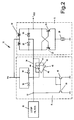
- the embodiment of the voltage-controlled oscillator 12 is represented in more detail in figure 2. It comprises the oscillator circuit section S.
- This circuit section S contains two bipolar transistors 22, 24, whose interconnected emitters are grounded via a current source 26.
- the base of both transistors 22, 24 is connected to the collector of the opposite transistor in each case.
- the collector of each of the transistors 22, 24 is connected to the cathode of varicap diodes 28 and 30, respectively, whose anodes are interconnected.
- Connected in parallel with these two varicap diodes 28, 30 is a coil 32 whose centre tap is connected to the supply voltage Vcc.
- the control voltage supplied by the loop filter 20 is applied to the interconnected anodes of both varicap diodes 28, 30 by way of the control line 34, by means of which the frequency f VCO , generated by the oscillator 12, can be determined.
- the voltage-controlled oscillator 12 furthermore comprises a compensation circuit K, containing two varicap diodes 36, 38, which are arranged in the same configuration as the varicap diodes 28, 30 in the circuit section S. This means that the cathodes are connected to the supply rail Vcc, and that the anodes are connected to each other.
- the compensation circuit K furthermore contains an operational amplifier 40 with a differential output, which, by connecting its inverting input 42 to the non-inverting output 44, is connected in a voltage-follower mode. The non-inverting input 41 of this operational amplifier 40 is connected to the control line 34.
- a field-effect transistor 48 Between the inverting output 46 of the operational amplifier 40 and ground is the drain/source path of a field-effect transistor 48, which, together with a further field-effect transistor 50, forms a current mirror.
- the drain/source path of the field-effect transistor 50 is between the control line 34 and ground.
- the gates of both the field-effect transistors 48 and 50 are connected to each other and to the inverting output 46 of the operational amplifier 40.
- the loop filter 20 supplies a control voltage via the control line 34 which causes the oscillator circuit section S to generate a specific output frequency f VCO .
- a temperature-related leakage current then flows through the varicap diodes 28, 30 which, without the action of the compensation circuit, would cause a change in the control voltage present in the control bus 34, and consequently also lead to a change of the frequency f VCO generated in the circuit section S.
- the operational amplifier connected in voltage follower mode, makes sure that exactly the same voltage is present at the varicap diodes 36 and 38 as at the varicap diodes 28, 30. This is achieved by having the operational amplifier 40 connected as a voltage follower, which means that the same voltage is present at its output 44 as is also applied to its non-inverting input 41. Since the same voltage is therefore present at the varicap diodes 36, 38 as well as at the varicap diodes 28, 30, the leakage current flowing at the same temperature will be the same. This leakage current also flows, via the inverting output 46 of the operational amplifier 40, through the field-effect transistor 48. Because of the current-mirroring effect, this leakage current will also flow through the field-effect transistor 50.
- the leakage current flowing through the field-effect transistor 50 is, therefore, subtracted from the current flowing through the varicap diodes 28, 30, so that it does not lead to a discharge of the capacitor contained in the loop filter 20, whose charge voltage constitutes the control voltage for the voltage-controlled oscillator 12.
- the leakage current through the varicap diodes 28, 30 therefore does not affect on the control voltage, instrumental in generating the desired output frequency f VCO .
- the circuit arrangement described therefore, compensates the temperature-dependent leakage current flowing through the varicap diodes 28, 30 in the voltage-controlled oscillator 12, thus ensuring that the oscillator 12 can generate the frequency f VCO , exclusively determined by the control voltage provided by the loop filter 20, even when the temperature conditions change.
Landscapes
- Stabilization Of Oscillater, Synchronisation, Frequency Synthesizers (AREA)
- Inductance-Capacitance Distribution Constants And Capacitance-Resistance Oscillators (AREA)
Applications Claiming Priority (2)
| Application Number | Priority Date | Filing Date | Title |
|---|---|---|---|
| DE10110095A DE10110095C1 (de) | 2001-03-02 | 2001-03-02 | Schaltungsanordnung zur Leckstromkompensation in einem spannungsgesteuerten Oszillator einer PLL-Schaltung |
| DE10110095 | 2001-03-02 |
Publications (3)
| Publication Number | Publication Date |
|---|---|
| EP1237283A2 true EP1237283A2 (de) | 2002-09-04 |
| EP1237283A3 EP1237283A3 (de) | 2004-09-22 |
| EP1237283B1 EP1237283B1 (de) | 2008-11-05 |
Family
ID=7676078
Family Applications (1)
| Application Number | Title | Priority Date | Filing Date |
|---|---|---|---|
| EP02003142A Expired - Lifetime EP1237283B1 (de) | 2001-03-02 | 2002-02-14 | Schaltungsanordnung zur Kompensierung von Leckströmen in einem spannungsgesteuerten Oszillator einer PLL-Schaltung |
Country Status (4)
| Country | Link |
|---|---|
| US (1) | US6593818B2 (de) |
| EP (1) | EP1237283B1 (de) |
| JP (2) | JP2002314412A (de) |
| DE (2) | DE10110095C1 (de) |
Cited By (3)
| Publication number | Priority date | Publication date | Assignee | Title |
|---|---|---|---|---|
| WO2003100980A1 (en) * | 2002-05-28 | 2003-12-04 | Koninklijke Philips Electronics N.V. | Pll circuit |
| WO2005020438A1 (en) * | 2003-08-11 | 2005-03-03 | Rambus Inc. | Leakage compensation for filter capacitors in phase-locked loops |
| KR20200011877A (ko) | 2018-07-25 | 2020-02-04 | 쟈인 에레쿠토로닉스 가부시키가이샤 | 전압 제어 발진기, pll 회로 및 cdr 장치 |
Families Citing this family (5)
| Publication number | Priority date | Publication date | Assignee | Title |
|---|---|---|---|---|
| US6954088B2 (en) * | 2003-11-25 | 2005-10-11 | International Business Machines Corporation | Voltage controlled oscillator (VCO) with amplitude control |
| CN100458639C (zh) * | 2007-03-20 | 2009-02-04 | 北京中星微电子有限公司 | 一种补偿mos器件栅极漏电流的装置及方法 |
| JP5799828B2 (ja) * | 2011-04-12 | 2015-10-28 | 株式会社ソシオネクスト | 位相ロックループ回路 |
| US9163954B2 (en) * | 2011-12-29 | 2015-10-20 | Stmicroelectronics Asia Pacific Pte Ltd | Leakage current compensation circuit |
| EP3945681B1 (de) | 2020-07-30 | 2025-09-03 | Socionext Inc. | Leckstromkompensation |
Family Cites Families (7)
| Publication number | Priority date | Publication date | Assignee | Title |
|---|---|---|---|---|
| US4191976A (en) * | 1978-09-26 | 1980-03-04 | Data General Corporation | Circuit indicating phase relationship |
| US5254958A (en) * | 1991-02-19 | 1993-10-19 | Pacific Communications, Inc. | Phase-lock-loop circuit and method for compensating, data bias in the same |
| US5598405A (en) * | 1994-01-25 | 1997-01-28 | Alps Electric Co., Ltd. | Time division multiple access time division duplex type transmitter-receiver |
| US5659588A (en) * | 1996-08-15 | 1997-08-19 | Lsi Logic Corporation | Phase-locked loop having filter leakage cancellation circuit |
| FR2755556A1 (fr) * | 1996-11-06 | 1998-05-07 | Motorola Semiconducteurs | Modulateur de frequence, emetteur et emetteur-recepteur incorporant ce modulateur de frequence |
| DE19812972B4 (de) * | 1998-03-24 | 2004-02-12 | Rohde & Schwarz Gmbh & Co. Kg | Integratorschaltung |
| SE516140C2 (sv) * | 1999-09-07 | 2001-11-26 | Ericsson Telefon Ab L M | Förfarande och anordning för att låsa en styrspänning till en spänningsstyrd oscillator |
-
2001
- 2001-03-02 DE DE10110095A patent/DE10110095C1/de not_active Expired - Fee Related
-
2002
- 2002-02-14 DE DE60229681T patent/DE60229681D1/de not_active Expired - Lifetime
- 2002-02-14 EP EP02003142A patent/EP1237283B1/de not_active Expired - Lifetime
- 2002-03-01 US US10/087,299 patent/US6593818B2/en not_active Expired - Lifetime
- 2002-03-01 JP JP2002055413A patent/JP2002314412A/ja not_active Withdrawn
-
2008
- 2008-06-30 JP JP2008170981A patent/JP2008271599A/ja not_active Abandoned
Cited By (6)
| Publication number | Priority date | Publication date | Assignee | Title |
|---|---|---|---|---|
| WO2003100980A1 (en) * | 2002-05-28 | 2003-12-04 | Koninklijke Philips Electronics N.V. | Pll circuit |
| US7116177B2 (en) | 2002-05-28 | 2006-10-03 | Koninklijke Philips Electronics N.V. | PLL circuit leakage compensation circuit for generating a leakage compensation signal |
| WO2005020438A1 (en) * | 2003-08-11 | 2005-03-03 | Rambus Inc. | Leakage compensation for filter capacitors in phase-locked loops |
| US6963232B2 (en) | 2003-08-11 | 2005-11-08 | Rambus, Inc. | Compensator for leakage through loop filter capacitors in phase-locked loops |
| US7248086B2 (en) | 2003-08-11 | 2007-07-24 | Rambus, Inc. | Leakage compensation for capacitors in loop filters |
| KR20200011877A (ko) | 2018-07-25 | 2020-02-04 | 쟈인 에레쿠토로닉스 가부시키가이샤 | 전압 제어 발진기, pll 회로 및 cdr 장치 |
Also Published As
| Publication number | Publication date |
|---|---|
| EP1237283A3 (de) | 2004-09-22 |
| JP2008271599A (ja) | 2008-11-06 |
| DE60229681D1 (de) | 2008-12-18 |
| US20020121939A1 (en) | 2002-09-05 |
| EP1237283B1 (de) | 2008-11-05 |
| US6593818B2 (en) | 2003-07-15 |
| DE10110095C1 (de) | 2002-06-20 |
| JP2002314412A (ja) | 2002-10-25 |
Similar Documents
| Publication | Publication Date | Title |
|---|---|---|
| US8558592B2 (en) | Charge pump and active filter for a feedback circuit | |
| US7161401B2 (en) | Wide output-range charge pump with active biasing current | |
| US6281758B1 (en) | Differential LC-VCO, charge pump, and loop filter architecture for improved noise-immunity in integrated phase-locked loops | |
| CN205195691U (zh) | 锁相环电路 | |
| CN101572549B (zh) | 自偏置锁相环和锁相方法 | |
| US8063678B2 (en) | Charge pump for phase locked loop | |
| US20050035797A1 (en) | Compensator for leakage through loop filter capacitors in phase-locked loops | |
| US6956417B2 (en) | Leakage compensation circuit | |
| JP2008271599A (ja) | Pll回路の電圧制御発振器における漏洩電流を補償する回路構成 | |
| FI97579C (fi) | Vaihelukitun silmukan silmukkasuodatin | |
| US20080136472A1 (en) | Power supply circuit for a phase-locked loop | |
| US10985767B2 (en) | Phase-locked loop circuitry having low variation transconductance design | |
| US10291238B2 (en) | Semiconductor device and PLL circuit | |
| US8432200B1 (en) | Self-tracking adaptive bandwidth phase-locked loop | |
| US6265946B1 (en) | Differential mode charge pump and loop filter with common mode feedback | |
| JP4482524B2 (ja) | リーク電流補償回路を備えたpll回路 | |
| US8531218B1 (en) | Frequency generating system | |
| US20090189650A1 (en) | PLL circuit including voltage controlled oscillator having voltage-current conversion circuit | |
| US7750741B2 (en) | PLL circuit and semiconductor device | |
| US6677789B1 (en) | Rail-to-rail linear charge pump | |
| US12512844B2 (en) | Voltage-current conversion circuit, a voltage-controlled oscillator, and a phase-locked loop circuit | |
| US12355451B1 (en) | Phase locked loop filter circuitry | |
| KR100971165B1 (ko) | 위상 동기 루프의 루프-필터의 튜닝 | |
| JP3105823B2 (ja) | 電圧電流変換回路 | |
| JP2000013220A (ja) | 位相同期回路 |
Legal Events
| Date | Code | Title | Description |
|---|---|---|---|
| PUAI | Public reference made under article 153(3) epc to a published international application that has entered the european phase |
Free format text: ORIGINAL CODE: 0009012 |
|
| AK | Designated contracting states |
Kind code of ref document: A2 Designated state(s): AT BE CH CY DE DK ES FI FR GB GR IE IT LI LU MC NL PT SE TR |
|
| AX | Request for extension of the european patent |
Free format text: AL;LT;LV;MK;RO;SI |
|
| PUAL | Search report despatched |
Free format text: ORIGINAL CODE: 0009013 |
|
| AK | Designated contracting states |
Kind code of ref document: A3 Designated state(s): AT BE CH CY DE DK ES FI FR GB GR IE IT LI LU MC NL PT SE TR |
|
| AX | Request for extension of the european patent |
Extension state: AL LT LV MK RO SI |
|
| 17P | Request for examination filed |
Effective date: 20050316 |
|
| AKX | Designation fees paid |
Designated state(s): DE FR GB |
|
| 17Q | First examination report despatched |
Effective date: 20060519 |
|
| GRAP | Despatch of communication of intention to grant a patent |
Free format text: ORIGINAL CODE: EPIDOSNIGR1 |
|
| GRAS | Grant fee paid |
Free format text: ORIGINAL CODE: EPIDOSNIGR3 |
|
| GRAA | (expected) grant |
Free format text: ORIGINAL CODE: 0009210 |
|
| AK | Designated contracting states |
Kind code of ref document: B1 Designated state(s): DE FR GB |
|
| REG | Reference to a national code |
Ref country code: GB Ref legal event code: FG4D |
|
| REF | Corresponds to: |
Ref document number: 60229681 Country of ref document: DE Date of ref document: 20081218 Kind code of ref document: P |
|
| PLBE | No opposition filed within time limit |
Free format text: ORIGINAL CODE: 0009261 |
|
| STAA | Information on the status of an ep patent application or granted ep patent |
Free format text: STATUS: NO OPPOSITION FILED WITHIN TIME LIMIT |
|
| 26N | No opposition filed |
Effective date: 20090806 |
|
| REG | Reference to a national code |
Ref country code: FR Ref legal event code: PLFP Year of fee payment: 15 |
|
| REG | Reference to a national code |
Ref country code: FR Ref legal event code: PLFP Year of fee payment: 16 |
|
| REG | Reference to a national code |
Ref country code: FR Ref legal event code: PLFP Year of fee payment: 17 |
|
| PGFP | Annual fee paid to national office [announced via postgrant information from national office to epo] |
Ref country code: GB Payment date: 20180125 Year of fee payment: 17 Ref country code: DE Payment date: 20180207 Year of fee payment: 17 |
|
| PGFP | Annual fee paid to national office [announced via postgrant information from national office to epo] |
Ref country code: FR Payment date: 20180118 Year of fee payment: 17 |
|
| REG | Reference to a national code |
Ref country code: DE Ref legal event code: R119 Ref document number: 60229681 Country of ref document: DE |
|
| GBPC | Gb: european patent ceased through non-payment of renewal fee |
Effective date: 20190214 |
|
| PG25 | Lapsed in a contracting state [announced via postgrant information from national office to epo] |
Ref country code: DE Free format text: LAPSE BECAUSE OF NON-PAYMENT OF DUE FEES Effective date: 20190903 Ref country code: GB Free format text: LAPSE BECAUSE OF NON-PAYMENT OF DUE FEES Effective date: 20190214 |
|
| PG25 | Lapsed in a contracting state [announced via postgrant information from national office to epo] |
Ref country code: FR Free format text: LAPSE BECAUSE OF NON-PAYMENT OF DUE FEES Effective date: 20190228 |