EP1237204B1 - Elément à couche piézoélectrique/électrostrictif - Google Patents
Elément à couche piézoélectrique/électrostrictif Download PDFInfo
- Publication number
- EP1237204B1 EP1237204B1 EP02251448A EP02251448A EP1237204B1 EP 1237204 B1 EP1237204 B1 EP 1237204B1 EP 02251448 A EP02251448 A EP 02251448A EP 02251448 A EP02251448 A EP 02251448A EP 1237204 B1 EP1237204 B1 EP 1237204B1
- Authority
- EP
- European Patent Office
- Prior art keywords
- piezoelectric
- electrostrictive film
- lower electrode
- electrostrictive
- electrode
- Prior art date
- Legal status (The legal status is an assumption and is not a legal conclusion. Google has not performed a legal analysis and makes no representation as to the accuracy of the status listed.)
- Expired - Lifetime
Links
- 239000000463 material Substances 0.000 claims description 28
- 239000000758 substrate Substances 0.000 claims description 27
- 239000000919 ceramic Substances 0.000 claims description 15
- 239000010408 film Substances 0.000 description 84
- 238000010438 heat treatment Methods 0.000 description 18
- 238000000034 method Methods 0.000 description 15
- 239000012530 fluid Substances 0.000 description 12
- BASFCYQUMIYNBI-UHFFFAOYSA-N platinum Chemical compound [Pt] BASFCYQUMIYNBI-UHFFFAOYSA-N 0.000 description 8
- 229910010252 TiO3 Inorganic materials 0.000 description 5
- 239000007788 liquid Substances 0.000 description 5
- 230000008569 process Effects 0.000 description 5
- 238000007650 screen-printing Methods 0.000 description 5
- QAOWNCQODCNURD-UHFFFAOYSA-N Sulfuric acid Chemical compound OS(O)(=O)=O QAOWNCQODCNURD-UHFFFAOYSA-N 0.000 description 4
- 230000015572 biosynthetic process Effects 0.000 description 4
- 230000008859 change Effects 0.000 description 4
- 238000006073 displacement reaction Methods 0.000 description 4
- 239000011521 glass Substances 0.000 description 4
- 229910052697 platinum Inorganic materials 0.000 description 4
- 230000001133 acceleration Effects 0.000 description 3
- 239000000956 alloy Substances 0.000 description 3
- 229910045601 alloy Inorganic materials 0.000 description 3
- 230000005684 electric field Effects 0.000 description 3
- KDLHZDBZIXYQEI-UHFFFAOYSA-N Palladium Chemical compound [Pd] KDLHZDBZIXYQEI-UHFFFAOYSA-N 0.000 description 2
- 239000012141 concentrate Substances 0.000 description 2
- 239000004020 conductor Substances 0.000 description 2
- 238000005336 cracking Methods 0.000 description 2
- 238000009792 diffusion process Methods 0.000 description 2
- RVTZCBVAJQQJTK-UHFFFAOYSA-N oxygen(2-);zirconium(4+) Chemical compound [O-2].[O-2].[Zr+4] RVTZCBVAJQQJTK-UHFFFAOYSA-N 0.000 description 2
- 239000011347 resin Substances 0.000 description 2
- 229920005989 resin Polymers 0.000 description 2
- 238000009751 slip forming Methods 0.000 description 2
- 238000004544 sputter deposition Methods 0.000 description 2
- 230000036962 time dependent Effects 0.000 description 2
- XLYOFNOQVPJJNP-UHFFFAOYSA-N water Substances O XLYOFNOQVPJJNP-UHFFFAOYSA-N 0.000 description 2
- 229910001928 zirconium oxide Inorganic materials 0.000 description 2
- LFQSCWFLJHTTHZ-UHFFFAOYSA-N Ethanol Chemical compound CCO LFQSCWFLJHTTHZ-UHFFFAOYSA-N 0.000 description 1
- 229910003334 KNbO3 Inorganic materials 0.000 description 1
- 229910052581 Si3N4 Inorganic materials 0.000 description 1
- BQCADISMDOOEFD-UHFFFAOYSA-N Silver Chemical compound [Ag] BQCADISMDOOEFD-UHFFFAOYSA-N 0.000 description 1
- 230000002411 adverse Effects 0.000 description 1
- 230000004075 alteration Effects 0.000 description 1
- 239000007864 aqueous solution Substances 0.000 description 1
- 239000000470 constituent Substances 0.000 description 1
- PMHQVHHXPFUNSP-UHFFFAOYSA-M copper(1+);methylsulfanylmethane;bromide Chemical compound Br[Cu].CSC PMHQVHHXPFUNSP-UHFFFAOYSA-M 0.000 description 1
- KZHJGOXRZJKJNY-UHFFFAOYSA-N dioxosilane;oxo(oxoalumanyloxy)alumane Chemical compound O=[Si]=O.O=[Si]=O.O=[Al]O[Al]=O.O=[Al]O[Al]=O.O=[Al]O[Al]=O KZHJGOXRZJKJNY-UHFFFAOYSA-N 0.000 description 1
- 238000007598 dipping method Methods 0.000 description 1
- 239000007772 electrode material Substances 0.000 description 1
- 239000007789 gas Substances 0.000 description 1
- 230000006872 improvement Effects 0.000 description 1
- 229910010272 inorganic material Inorganic materials 0.000 description 1
- 239000011147 inorganic material Substances 0.000 description 1
- 239000012212 insulator Substances 0.000 description 1
- 238000007733 ion plating Methods 0.000 description 1
- 238000010884 ion-beam technique Methods 0.000 description 1
- CPLXHLVBOLITMK-UHFFFAOYSA-N magnesium oxide Inorganic materials [Mg]=O CPLXHLVBOLITMK-UHFFFAOYSA-N 0.000 description 1
- 239000000395 magnesium oxide Substances 0.000 description 1
- AXZKOIWUVFPNLO-UHFFFAOYSA-N magnesium;oxygen(2-) Chemical compound [O-2].[Mg+2] AXZKOIWUVFPNLO-UHFFFAOYSA-N 0.000 description 1
- 238000005259 measurement Methods 0.000 description 1
- 238000002156 mixing Methods 0.000 description 1
- 239000000203 mixture Substances 0.000 description 1
- 229910052863 mullite Inorganic materials 0.000 description 1
- 239000003921 oil Substances 0.000 description 1
- 239000011368 organic material Substances 0.000 description 1
- 239000003960 organic solvent Substances 0.000 description 1
- TWNQGVIAIRXVLR-UHFFFAOYSA-N oxo(oxoalumanyloxy)alumane Chemical compound O=[Al]O[Al]=O TWNQGVIAIRXVLR-UHFFFAOYSA-N 0.000 description 1
- 229910052763 palladium Inorganic materials 0.000 description 1
- 230000036961 partial effect Effects 0.000 description 1
- 238000007747 plating Methods 0.000 description 1
- 230000009257 reactivity Effects 0.000 description 1
- 229910052703 rhodium Inorganic materials 0.000 description 1
- 239000010948 rhodium Substances 0.000 description 1
- MHOVAHRLVXNVSD-UHFFFAOYSA-N rhodium atom Chemical compound [Rh] MHOVAHRLVXNVSD-UHFFFAOYSA-N 0.000 description 1
- HQVNEWCFYHHQES-UHFFFAOYSA-N silicon nitride Chemical compound N12[Si]34N5[Si]62N3[Si]51N64 HQVNEWCFYHHQES-UHFFFAOYSA-N 0.000 description 1
- 229910052709 silver Inorganic materials 0.000 description 1
- 239000004332 silver Substances 0.000 description 1
- 238000005245 sintering Methods 0.000 description 1
- 239000002002 slurry Substances 0.000 description 1
- 238000005507 spraying Methods 0.000 description 1
- 239000000126 substance Substances 0.000 description 1
- 239000010409 thin film Substances 0.000 description 1
- 238000001771 vacuum deposition Methods 0.000 description 1
- 238000009834 vaporization Methods 0.000 description 1
- 230000008016 vaporization Effects 0.000 description 1
Images

Classifications
-
- H—ELECTRICITY
- H10—SEMICONDUCTOR DEVICES; ELECTRIC SOLID-STATE DEVICES NOT OTHERWISE PROVIDED FOR
- H10N—ELECTRIC SOLID-STATE DEVICES NOT OTHERWISE PROVIDED FOR
- H10N30/00—Piezoelectric or electrostrictive devices
- H10N30/20—Piezoelectric or electrostrictive devices with electrical input and mechanical output, e.g. functioning as actuators or vibrators
- H10N30/204—Piezoelectric or electrostrictive devices with electrical input and mechanical output, e.g. functioning as actuators or vibrators using bending displacement, e.g. unimorph, bimorph or multimorph cantilever or membrane benders
- H10N30/2047—Membrane type
-
- B—PERFORMING OPERATIONS; TRANSPORTING
- B41—PRINTING; LINING MACHINES; TYPEWRITERS; STAMPS
- B41J—TYPEWRITERS; SELECTIVE PRINTING MECHANISMS, i.e. MECHANISMS PRINTING OTHERWISE THAN FROM A FORME; CORRECTION OF TYPOGRAPHICAL ERRORS
- B41J2/00—Typewriters or selective printing mechanisms characterised by the printing or marking process for which they are designed
- B41J2/005—Typewriters or selective printing mechanisms characterised by the printing or marking process for which they are designed characterised by bringing liquid or particles selectively into contact with a printing material
- B41J2/01—Ink jet
- B41J2/135—Nozzles
- B41J2/14—Structure thereof only for on-demand ink jet heads
- B41J2002/14491—Electrical connection
Definitions
- the present invention relates to piezoelectric/electrostrictive film elements, and in particular to piezoelectric/electrostrictive elements employed as actuators utilizing flexural displacement and sensors for detecting fluid properties, sound pressures, minute weights, acceleration, and so on., as for example, in microphones or viscosity sensors.
- Piezoelectric/electrostrictive film elements have conventionally been used as actuators and various types of sensors.
- a piezoelectric/electrostrictive film element used as a sensor is used for measuring the properties of a fluid such as the density, concentration, and viscosity as disclosed in Japanese Patent publication No. 5-201265A.
- Such elements are used as sensors because there is a correlation between the amplitude of a piezoelectric oscillator and the viscosity resistance of a fluid in contact with the oscillator.
- a modes of vibration in a mechanical system such as the vibration of an oscillator can be converted to an equivalent circuit in an electrical system.
- a piezoelectric/electrostrictive oscillator vibrates in a fluid, and receives a mechanical resistance based on the viscosity resistance of the fluid.
- the oscillator thereby senses the variation of an electrical constant of an equivalent electrical circuit of the piezoelectric /electrostrictive element of the oscillator.
- various parameters which include the viscosity, density, and concentration of the fluid.
- Fluids that can be measured include liquids and gases and include not only liquids consisting of a single component such as water, alcohol, and oils but also fluids composed of slurries, and pastes obtained by dissolving, mixing or suspending soluble or insolublemedia.
- Electrical constants to be detected include loss factor, phase, resistance, reactance, conductance, susceptance, inductance, and capacitance.
- preferred electrical constants are loss factors and phase because they have a single maximum or minimum point of variation near a resonance frequency of an equivalent circuit. This makes it possible to measure not only the viscosity of a fluid but also the density and concentration of the same. For example, the concentration of sulfuric acid in an aqueous solution of sulfuric acid can be measured through the use of the above electrical constants.
- the variation in resonance frequency may also be utilized as an index for sensing variations in the mode of vibration, if there are no specific problems from the standpoint of precision of measurement and durability.
- a known piezoelectric/electrostrictive film element is also disclosed in EP-A-615294.
- an auxiliary electrode is formed at a position independent of a lower electrode on a substrate which is made of ceramic having a thin diaphragm portion and thick portion on the periphery thereof.
- a portion of the auxiliary electrode is positioned beneath a piezoelectric/electrostrictive film.
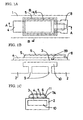
- a piezoelectric/electrostrictive film element described in EP-A-1154497 (published 14.11.2001) is in present Figs. 3A, 3B and 3C.
- a piezoelectric/electrostrictive film 5 is on a lower electrode 4 and is of a size that the surrounding portion of the piezoelectric/electrostrictive film 5 extends beyond the electrode 4 such that the periphery of the piezoelectric/electrostrictive film 5 projects above the ceramic substrate 1.
- an extending portion 11 of the piezoelectric/electrostrictive film 5 can manifest sufficient flexural displacement, generation and vibration because it is in an incompletely bonded state with the substrate 1.
- the extended portion 11 is not bonded with the substrate due to the presence of incompletely bonded portions 7A.
- An incompletely bonded state means that a portion of the extended portion 11 is either partially bonded with the ceramic substrate or that a portion an unbonded region without any bonded portion is in existence. Specifically, it is defined to mean that the peeling (tear off) strength of the film 5 to substrate 1 is 0.5 kg/mm 2 or less.
- the formation of in unbonded state as described above there are instances when it is necessary to have a low reactivity between the materials selected for the substrate and the piezoelectric/electrostrictive film.
- the dummy layer is formed by a stamping method, a screen printing method or an ink jet method.
- the incompletely bonded portion 7A is formed when the dummy layer is subsequently dissolved.
- the dummy layer is fabricated with combustible/removable materials, such as resin materials, which are dissolved away to form the incompletely bonded portions 7A when the piezoelectric/electrostrictive film 5 is heat treated.
- the dummy layer is formed with a resin material to be dissolved in a composition such as water or organic solvents, etc. Accordingly, after the formation of either the piezoelectric/electrostrictive film alone or in conjunction with the upper electrode 6, the incompletely bonded portions 7A is formed by dissolving or removing the dummy layer.
- an incompletely bonded portion 7B is formed over a thin diaphragm 3 and a thick portion of a substrate between a lower electrode 4 and an auxiliary electrode 8 as shown in Fig. 3B.
- the incompletely bonded portion 7B is in an incompletely bonded state similarly to the incompletely bonded portion 7A of the extended portion 11.
- a time-passage variation or change in the incompletely bonded state of an incompletely bonded portion 7B is one of major factors that cause a change in a mode of variation, in the case of a sensor element or the like utilizing electrical constants during vibration.
- the incompletely bonded portion that has a low bonding force and low mechanical strength extends over the thin diaphragm and the thick portion. Since the thin diaphragm undergoes vibration or displacement and the thick portion is fixed, the incompletely bonded state cannot be established with high reproducibility and stability because of phenomena such as partial unbonded and micro-cracks. The micro-cracks thus generated can develop into a greater crack which can cause the piezoelectric/electrostrictive film to crack.
- the piezoelectric/electrostrictive film sandwiched by the lower electrode and upper electrode continuously extends over the thin diaphragm and the thick portion.
- an electric field generated during a process of polarizing or driving the element will be applied to the region extending over the thin diaphragm and thick portion. It was found that this piezoelectrically activates edges of the thin diaphragm portion where stresses are likely to concentrate generate an additional stress that can result a crack.
- EP-A-976560 shows structures similar to those of EP-A-615 294, in which an auxiliary electrode in some cases extends from a thick portion of the substrate onto the thin diaphragm.
- the present invention provides a piezoelectric/electrostrictive film element as set out in claim 1.
- a piezoelectrically and electrostrictively active portion of the piezoelectric/electrostrictive film that is sandwiched between the upper electrode and the lower electrode is preferably located only over the thin diaphragm portion.
- a bonding layer for bonding the piezoelectric/electrostrictive film and the thin diaphragm portion is provided between the lower electrode and the auxiliary electrode.
- Fig. 1 illustrates an embodiment of a piezoelectric/electrostrictive film element for a sensor according to the present invention.
- Fig. 2 illustrates another embodiment of a piezoelectric/electrostrictive film element for a sensor according to the present invention.
- Figs. 3A, 3B, and 3C illustrate a conventional piezoelectric/electrostrictive film element discussed above.
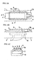
- Figs. 1A, 1B, and 1C show a piezoelectric/electrostrictive film element for a sensor that is an embodiment of the invention.
- a piezoelectric/ electrostrictive oscillator is formed as an integral structure in which a lower electrode 4, a piezoelectric/electrostrictive film 5, and an upper electrode 6 are sequentially formed on a ceramic substrate 1
- the substrate 1 comprises of a thin diaphragm portion 3 and thick portions 2 using a normal method of forming films.
- the lower electrode 4 is formed in a length at which one end of the same close to an auxiliary electrode 8 does not extend beyond the thin diaphragm portion 3.
- the auxiliary electrode 8 is formed on the same plane on which the lower electrode 4 is located.
- the auxiliary electrode is at a position of the thin diaphragm portion independent of the lower electrode such that it extends beneath the piezoelectric/electrostrictive film 5.
- the auxiliary electrode 8 is continuously formed with a predetermined length to extend from a thick portion 2 opposite to the lower electrode 4 to the thin diaphragm portion 3.
- the piezoelectric/ electrostrictive film 5 is formed over the lower electrode 4 and the auxiliary electrode 8.
- the upper electrode 6 is formed over the piezoelectric/electrostrictive film 5 and the auxiliary electrode 8 to be in continuity to the auxiliary electrode 8.
- An incompletely bonded portion 7B is provided in proximity to only the thin diaphragm portion 3.
- An extending portion 11 is not always present in the present invention, and the lower electrode 4 and piezoelectric/electrostrictive film 5 may be substantially the same size when seeking to reduce the variations in the electrical constants and the variation of the element properties over time.
- the ceramic substrate 1 is preferably made of a material having heat resistance, chemical stability, and insulating properties.
- the reason for applying the above material is that a heat treatment may be performed when the lower electrode 4, piezoelectric/electrostrictive film 5, and upper electrode 6 are integrated.
- the piezoelectric/electrostrictive film element as a sensor element may be used to sense the properties of a conductive and corrosive liquid, as will be described later.
- ceramics that can be used include stabilized zirconium oxide, aluminum oxide, magnesium oxide, mullite, aluminum nitride, silicon nitride, and glass.
- stabilized zirconium oxide is preferably used for reasons including its excellent toughness and its capability of maintaining high mechanical strength when the thin diaphragm portion is formed.
- the thickness of the thin diaphragmportion 3 of the ceramic substrate 1 is 50 ⁇ m or less in general, preferably 30 ⁇ m or less and, more preferably 15 ⁇ m or less in order not to hinder the vibration of the piezoelectric/electrostrictive film.
- the thin diaphragm portion may have any surface configuration such as a rectangular, square, triangular, elliptic, or completely round configuration.
- a rectangular or completely round configuration is chosen as occasion demands when the element is used as a sensor element in which the resonant mode to be excited must be simple.
- the lower electrode 4 and auxiliary electrode 8 are formed on a surface of such a ceramic substrate 1.
- the lower electrode 4 is formed with a predetermined size that is equal to or smaller than the size of the piezoelectric/electrostrictive film 5 such that it extends from one end of the ceramic substrate on to the thin diaphragm portion 3.
- the auxiliary electrode 8 is formed such that it continuously extends from the end of the ceramic substrate 1 opposite to the lower electrode 4 to a predetermined position on the thin diaphragm portion 3.
- the ends of the lower electrode 4 and auxiliary electrode 8 on the thick portions are used as lead terminals.
- the lower electrode 4 and auxiliary electrode 8 may be made of different materials or the same material, and a conductive material that can be well bonded to both of the ceramic substrate 1 and piezoelectric/electrostrictive film 5 is used. Specifically, platinum, palladium, rhodium, silver, or an electrode material primarily constituted by an alloy of such elements is preferably used. Especially, when a heat treatment for sintering is performed when the piezoelectric/electrostrictive film is formed, platinum and an alloy primarily constituted by the same are preferably used.
- the lower electrode 4 and auxiliary electrode 8 are formed using various known methods for forming films. Specifically, while methods for forming thin films such as ion beam, sputtering, vacuum deposition, CVD, ion plating, and plating and methods for forming thick films such as screen printing, spraying, and dipping are appropriately selected, and sputtering and screen printing are preferably selected above all.
- a bonding layer 7C is formed in the position of an incompletely bonded portion 7B before forming the piezoelectric/electrostrictive film 5.
- the bonding layer 7C comprising an insulator may be made of either organic or inorganic material as long as it can be well bonded to and bonded with both of the piezoelectric/electrostrictive film 5 and ceramic substrate 1.
- the thermal expansion factor of the material used as the bonding layer 7C is preferably in the middle of the thermal expansion factor of the substrate material and one of the material used for the piezoelectric/electrostricitve film 5.
- a glass material is preferably used to form the bonding layer 7C because it can be well bonded to and bonded with both of the piezoelectric/electrostrictive film 5 and ceramic substrate 1.
- a glass material having a softening point equal to or higher than the temperature of the heat treatment on the piezoelectric/electrostrictive film 5 is more preferably used. The reason is that such a glassmaterial bonds the piezoelectric/electrostrictive film 5 and substrate 1 more rigidly, and it is less vulnerable to deformation as a result of the heat treatment because of its high softening point.
- the piezoelectric/electrostrictive film 5 is made of (1-x) (Bi 0.5 Na 0.5 )TiO 3 -xKNbO 3 (x represents a molar fraction that satisfies 0 ⁇ x ⁇ 0.06) to be described later, e.g. (Bi 0.5 Na 0.5 )TiO 3 , or a material primarily constituted by the same.
- a material primarily constituted by (1-x) (Bi 0.5 Na 0.5 )TiO 3 -xKNbO 3 (x represents a molar fraction that satisfies 0.08 ⁇ x ⁇ 0.5) is preferably used to form the bonding layer 7C because the layer will be well bonded to both of the piezoelectric/electrostrictive film 5 and ceramic substrate 1 and will prevent the piezoelectric/ electrostrictive film 5 and substrate 1 from being adversely affected by the heat treatment.
- the bonding layer 7C is formed from (1-x) (Bi 0.5 Na 0.5 )TiO 3 -xKNbO 3 (x represents a molar faction that satisfies 0.08 ⁇ x ⁇ 0.5), it is well bonded to the piezoelectric/electrostrictive film 5 because it has components similar to those in the piezoelectric/electrostrictive film 5. Additionally, it is less vulnerable to problems caused by diffusion of different kinds of elements that are likely to occur when glass is used. Moreover, it well reacts with the substrate to allow rigid bonding because a great amount of KNbO 3 is included.
- a normal method for forming thick films, in particular, stamping process or screen printing process is used for forming a bonding layer 7C.
- An inkjet process is preferably used when the size of the region to be formed is in the range from about several tens ⁇ m to several hundred ⁇ m.
- the heat treatment may be performed before the piezoelectric/electrostricitve film 5 is formed. Alternatively, the heat treatment may be performed concurrently with the formation of the piezoelectric/electrostrictive film 5.
- the piezoelectric/electrostrictive film 5 is formed such that it extends over the lower electrode 4, auxiliary electrode 8, and bonding layer 7C with a size to cover the lower electrode 4.
- (Bi 0.5 Na 0.5 )TiO 3 or a material primarily constituted by the same is preferably used for the film 5 because the material can be bonded to the electrodes more excellently and the material results in reduced variation of the characteristics of the element to provide high reliability.
- (1-x) (Bi 0.5 Na 0.5 )TiO 3 -xKNbO 3 (x represents a molar fraction that satisfies 0 ⁇ x ⁇ 0.06) or a material primarily constituted by the same is more preferably used because it has relatively high piezoelectric characteristics.
- Such a piezoelectric/electrostrictive material is formed into the piezoelectric/electrostrictive film 5 using various known methods for forming films similarly to the lower electrode 4 and auxiliary electrode 8. Above all, screen-printing is preferably used because of low cost.
- the piezoelectric/electrostrictive film 5 thus formed is subjected to a heat treatment as occasion demands and is integrated with the lower electrode 4, auxiliary electrode 8, and bonding layer 7C.
- a bonding layer 7C more rigidly to suppress variation of the characteristics of the element to achieve higher reliability (Bi 0.5 Na 0.5 )TiO 3 or a material primarily constituted by the same is preferably used.
- (1-x) (Bi 0.5 Na 0.5 )TiO 3 - xKNbO 3 (x represents a molar fraction that satisfies 0 ⁇ x ⁇ 0.06) or a material primarily constituted by the same is used.
- those materials are preferably subjected to a heat treatment at a temperature in the range from 900°C to 1400°C and, more preferably, in the range from 1000°C to 1300°C.
- the heat treatment is preferably performed while controlling the source of vaporization of the piezoelectric/electrostrictive material and the atmosphere in order to prevent the piezoelectric/electrostrictive film 5 becoming unstable at high temperatures.
- the upper electrode 6 is continuously formed on the piezoelectric/electrostrictive film 5 thus formed such that it extends over the piezoelectric/electrostrictive film 5 and auxiliary electrode 8.
- the upper electrode 6 is made of a conductive material that can be well bonded to the piezoelectric/electrostrictive film 5, and is formed using the same method for forming films that is used for the lower electrode 4 and auxiliary electrode 8.
- the upper electrode 6 is subjected to a heat treatment, as occasion demands after it is formed and is bonded to the piezoelectric/electrostrictive film 5 and auxiliary electrode 8 to provide an integral structure.
- a heat treatment is inessential as it is for the lower electrode 4.
- the lower electrode 4, bonding layer, piezoelectric/electrostrictive film 5, and upper electrode 6 are bonded through a heat treatment, they may be subjected to the heat treatment each time they are formed or may be simultaneously subjected to the heat treatment after forming them sequentially.
- an appropriate temperature is chosen for the heat treatment to achieve high bondability and to suppress alteration as a result of diffusion of the constituent elements.
- the through holes 9 are formed in continuity to the cavity 10, there is no restriction on the structure below the cavity 10 inclusive in which the element is in contact with a fluid. It may be used any structure such as a simple cavity structure having no lid section.
- the piezoelectric/electrostrictive film 5 may have a length at which the end thereof closer to the auxiliary electrode 8 does not exceed the thin diaphragm portion 3 such that the film 5 does not extend over the thick portions 2.
- a piezoelectric/electrostrictive element in the first aspect of the invention provides stable element properties because the incompletely bonded portion that can cause variation and time-dependent changes is not structured to extend over the thin diaphragm portion and thick portions. As a result, the element can be used under any condition. Since it has a structure in which the incompletely bonded portion does not reside at the edge of the thin diaphragm where the piezoelectric/electrostrictive film is likely to crack, stresses are dispersed through the lower electrode or auxiliary electrode at the edge of the thin diaphragm portion.
- the element is able to completely prevent the piezoelectric/electrostrictive film from cracking regardless of the type and characteristics of the piezoelectric/electrostrictive film, It is therefore possible to obtain an element for determining the properties of a fluid and for discriminating between gasses and liquids by detecting electrical constants during vibration or an oscillator that reliably and stably works as an element for measuring sound pressures, very small weights, acceleration, and so on. Since a wide range of piezoelectric/electrostrictive materials can be chosen depending on required properties, there is provided advantages including easier improvement of properties and increased flexibility in designing.
- the piezoelectric/electrostrictive element in the second aspect of the invention completely prevents the piezoelectric/ electrostrictive film from cracking.
- the element has a structure in which the piezoelectrically and electrostrictively active portion of the piezoelectric/ electrostrictive film to which an electric field is applied resides only on the thin diaphragm portion.
- the piezoelectric/electrostrictive element in the third aspect of the invention it is possible to determine the properties of a fluid and for discriminate between gasses and liquids by detecting electrical constants during vibration, an element for measuring sound pressures, very small weights, acceleration, and so on.
Landscapes
- Piezo-Electric Transducers For Audible Bands (AREA)
- Transducers For Ultrasonic Waves (AREA)
- Compositions Of Oxide Ceramics (AREA)
- General Electrical Machinery Utilizing Piezoelectricity, Electrostriction Or Magnetostriction (AREA)
- Particle Formation And Scattering Control In Inkjet Printers (AREA)
Claims (3)
- Elément de film piézoélectrique/électrostrictif dans lequel (i) une électrode inférieure (4) conjointement avec une électrode auxiliaire (8), (ii) un film piézoélectrique/électrostrictif (5) et (iii) une électrode supérieure (6) sont formées séquentiellement sur un substrat (1) réalisé en céramique ayant une mince portion de membrane (3) avec des portions épaisses (2) sur sa périphérie, le film piézoélectrique/électrostrictif (5) s'étendant sur l'électrode inférieure (4) et l'électrode auxiliaire (8), caractérisé en ce que l'électrode inférieure (4) est formée de telle sorte qu'elle s'étend continuellement sur une portion épaisse (2) sur la périphérie et la portion de membrane mince (3); l'électrode auxiliaire (8) est formée de telle sorte qu'elle s'étend continuellement d'une position de la portion de membrane mince (3) indépendante de l'électrode inférieure à une portion épaisse opposée (2) sur la périphérie, et le matériau du film piézoélectrique (5) est, ou est constitué essentiellement de, (1-x) (Bi0,5Na0,5) TiO3-xKNbO3 où x est une fraction molaire satisfaisant à 0≦x≦0,06.
- Elément piézoélectrique/électrostrictif selon la revendication 1, où la portion piézoélectrique et électrostrictivement active du film piézoélectrique/électrostrictif (5) qui est prise en sandwich entre l'électrode supérieure (6) et l'électrode inférieure (4) se situe seulement sur la portion de membrane mince (3).
- Elément piézoélectrique/électrostrictif selon la revendication 1 ou 2, comprenant une couche de liaison (7C) pour relier le film piézoélectrique/électrostrictif (5) et la portion de membrane mince (3) réalisée entre l'électrode inférieure (4) et l'électrode auxiliaire (8).
Applications Claiming Priority (2)
| Application Number | Priority Date | Filing Date | Title |
|---|---|---|---|
| JP2001059118 | 2001-03-02 | ||
| JP2001059118A JP3728623B2 (ja) | 2001-03-02 | 2001-03-02 | 圧電/電歪膜型素子 |
Publications (3)
| Publication Number | Publication Date |
|---|---|
| EP1237204A2 EP1237204A2 (fr) | 2002-09-04 |
| EP1237204A3 EP1237204A3 (fr) | 2005-02-09 |
| EP1237204B1 true EP1237204B1 (fr) | 2006-09-13 |
Family
ID=18918734
Family Applications (1)
| Application Number | Title | Priority Date | Filing Date |
|---|---|---|---|
| EP02251448A Expired - Lifetime EP1237204B1 (fr) | 2001-03-02 | 2002-03-01 | Elément à couche piézoélectrique/électrostrictif |
Country Status (4)
| Country | Link |
|---|---|
| US (1) | US6541895B2 (fr) |
| EP (1) | EP1237204B1 (fr) |
| JP (1) | JP3728623B2 (fr) |
| DE (1) | DE60214617T2 (fr) |
Families Citing this family (12)
| Publication number | Priority date | Publication date | Assignee | Title |
|---|---|---|---|---|
| JP4038776B2 (ja) | 2003-02-10 | 2008-01-30 | セイコーエプソン株式会社 | 液体検出装置及び同装置を備えた液体容器 |
| KR100528350B1 (ko) * | 2004-02-27 | 2005-11-15 | 삼성전자주식회사 | 잉크젯 프린트헤드의 압전 액츄에이터 및 그 형성 방법 |
| US7126255B2 (en) | 2004-04-05 | 2006-10-24 | Ngk Insulators, Ltd. | Piezoelectric/electrostrictive film-type device |
| JP5009507B2 (ja) * | 2004-04-05 | 2012-08-22 | 日本碍子株式会社 | 圧電/電歪膜型素子 |
| JP4963159B2 (ja) | 2004-11-19 | 2012-06-27 | 日本碍子株式会社 | 圧電/電歪デバイス |
| JP2006147839A (ja) * | 2004-11-19 | 2006-06-08 | Ngk Insulators Ltd | 圧電/電歪デバイス |
| JP5004797B2 (ja) * | 2005-06-29 | 2012-08-22 | 日本碍子株式会社 | 圧電/電歪膜型素子 |
| CN100555697C (zh) * | 2005-06-29 | 2009-10-28 | 日本碍子株式会社 | 压电/电致伸缩元件的制造方法 |
| JP5031737B2 (ja) | 2006-04-24 | 2012-09-26 | 日本碍子株式会社 | 圧電/電歪膜型素子 |
| EP2037252A4 (fr) * | 2006-07-04 | 2012-10-24 | Ngk Insulators Ltd | Capteur à film piézoélectrique |
| US8261618B2 (en) * | 2010-11-22 | 2012-09-11 | General Electric Company | Device for measuring properties of working fluids |
| JP6133655B2 (ja) * | 2013-03-29 | 2017-05-24 | 日本碍子株式会社 | 圧電/電歪素子とその製造方法 |
Family Cites Families (8)
| Publication number | Priority date | Publication date | Assignee | Title |
|---|---|---|---|---|
| JP2665106B2 (ja) * | 1992-03-17 | 1997-10-22 | 日本碍子株式会社 | 圧電/電歪膜型素子 |
| JP3151644B2 (ja) * | 1993-03-08 | 2001-04-03 | 日本碍子株式会社 | 圧電/電歪膜型素子 |
| JP3521499B2 (ja) * | 1993-11-26 | 2004-04-19 | 日本碍子株式会社 | 圧電/電歪膜型素子 |
| JP3501860B2 (ja) * | 1994-12-21 | 2004-03-02 | 日本碍子株式会社 | 圧電/電歪膜型素子及びその製造方法 |
| US6004474A (en) * | 1997-03-28 | 1999-12-21 | Tdk Corporation | Piezoelectric ceramic composition |
| JP3648086B2 (ja) * | 1998-03-27 | 2005-05-18 | 日本碍子株式会社 | ZrO2磁器 |
| US6502928B1 (en) * | 1998-07-29 | 2003-01-07 | Seiko Epson Corporation | Ink jet recording head and ink jet recording apparatus comprising the same |
| JP3482939B2 (ja) * | 2000-05-09 | 2004-01-06 | 日本碍子株式会社 | 圧電/電歪膜型素子 |
-
2001
- 2001-03-02 JP JP2001059118A patent/JP3728623B2/ja not_active Expired - Fee Related
-
2002
- 2002-03-01 EP EP02251448A patent/EP1237204B1/fr not_active Expired - Lifetime
- 2002-03-01 DE DE60214617T patent/DE60214617T2/de not_active Expired - Lifetime
- 2002-03-04 US US10/090,411 patent/US6541895B2/en not_active Expired - Lifetime
Also Published As
| Publication number | Publication date |
|---|---|
| US20020158550A1 (en) | 2002-10-31 |
| EP1237204A3 (fr) | 2005-02-09 |
| JP2002261347A (ja) | 2002-09-13 |
| DE60214617T2 (de) | 2007-09-13 |
| US6541895B2 (en) | 2003-04-01 |
| JP3728623B2 (ja) | 2005-12-21 |
| DE60214617D1 (de) | 2006-10-26 |
| EP1237204A2 (fr) | 2002-09-04 |
Similar Documents
| Publication | Publication Date | Title |
|---|---|---|
| US6495945B2 (en) | Piezoelectric/electrostrictive element | |
| US7427820B2 (en) | Piezoelectric/electrostrictive film element | |
| EP1154497B1 (fr) | Composant à couche piézo-électrique/électrostrictive | |
| CN104764802B (zh) | 利用具有绝缘层的薄膜谐振器探测物质的装置和方法 | |
| EP1237204B1 (fr) | Elément à couche piézoélectrique/électrostrictif | |
| EP1659644B1 (fr) | Dispositif piézoélectrique/électrostrictif | |
| US7755253B2 (en) | Piezoelectric element and shape of an elecrode thereof | |
| US7183694B2 (en) | Piezoelectric/electrostrictive device | |
| US7126255B2 (en) | Piezoelectric/electrostrictive film-type device | |
| JP5009507B2 (ja) | 圧電/電歪膜型素子 | |
| JP4936909B2 (ja) | 流体特性測定装置の使用方法 |
Legal Events
| Date | Code | Title | Description |
|---|---|---|---|
| PUAI | Public reference made under article 153(3) epc to a published international application that has entered the european phase |
Free format text: ORIGINAL CODE: 0009012 |
|
| AK | Designated contracting states |
Kind code of ref document: A2 Designated state(s): AT BE CH CY DE DK ES FI FR GB GR IE IT LI LU MC NL PT SE TR |
|
| AX | Request for extension of the european patent |
Free format text: AL;LT;LV;MK;RO;SI |
|
| PUAL | Search report despatched |
Free format text: ORIGINAL CODE: 0009013 |
|
| RIC1 | Information provided on ipc code assigned before grant |
Ipc: 7H 01L 41/09 A Ipc: 7H 01L 41/047 B |
|
| AK | Designated contracting states |
Kind code of ref document: A3 Designated state(s): AT BE CH CY DE DK ES FI FR GB GR IE IT LI LU MC NL PT SE TR |
|
| AX | Request for extension of the european patent |
Extension state: AL LT LV MK RO SI |
|
| 17P | Request for examination filed |
Effective date: 20050502 |
|
| 17Q | First examination report despatched |
Effective date: 20050608 |
|
| AKX | Designation fees paid |
Designated state(s): DE FR GB IT |
|
| GRAP | Despatch of communication of intention to grant a patent |
Free format text: ORIGINAL CODE: EPIDOSNIGR1 |
|
| RIC1 | Information provided on ipc code assigned before grant |
Ipc: H01L 41/09 20060101AFI20060227BHEP Ipc: H01L 41/047 20060101ALI20060227BHEP |
|
| GRAS | Grant fee paid |
Free format text: ORIGINAL CODE: EPIDOSNIGR3 |
|
| GRAA | (expected) grant |
Free format text: ORIGINAL CODE: 0009210 |
|
| AK | Designated contracting states |
Kind code of ref document: B1 Designated state(s): DE FR GB IT |
|
| PG25 | Lapsed in a contracting state [announced via postgrant information from national office to epo] |
Ref country code: IT Free format text: LAPSE BECAUSE OF FAILURE TO SUBMIT A TRANSLATION OF THE DESCRIPTION OR TO PAY THE FEE WITHIN THE PRESCRIBED TIME-LIMIT;WARNING: LAPSES OF ITALIAN PATENTS WITH EFFECTIVE DATE BEFORE 2007 MAY HAVE OCCURRED AT ANY TIME BEFORE 2007. THE CORRECT EFFECTIVE DATE MAY BE DIFFERENT FROM THE ONE RECORDED. Effective date: 20060913 |
|
| REG | Reference to a national code |
Ref country code: GB Ref legal event code: FG4D |
|
| REF | Corresponds to: |
Ref document number: 60214617 Country of ref document: DE Date of ref document: 20061026 Kind code of ref document: P |
|
| ET | Fr: translation filed | ||
| PLBE | No opposition filed within time limit |
Free format text: ORIGINAL CODE: 0009261 |
|
| STAA | Information on the status of an ep patent application or granted ep patent |
Free format text: STATUS: NO OPPOSITION FILED WITHIN TIME LIMIT |
|
| 26N | No opposition filed |
Effective date: 20070614 |
|
| PGFP | Annual fee paid to national office [announced via postgrant information from national office to epo] |
Ref country code: IT Payment date: 20080322 Year of fee payment: 7 |
|
| PG25 | Lapsed in a contracting state [announced via postgrant information from national office to epo] |
Ref country code: IT Free format text: LAPSE BECAUSE OF NON-PAYMENT OF DUE FEES Effective date: 20090301 |
|
| PGFP | Annual fee paid to national office [announced via postgrant information from national office to epo] |
Ref country code: FR Payment date: 20130315 Year of fee payment: 12 Ref country code: GB Payment date: 20130225 Year of fee payment: 12 |
|
| PGFP | Annual fee paid to national office [announced via postgrant information from national office to epo] |
Ref country code: DE Payment date: 20140417 Year of fee payment: 13 |
|
| GBPC | Gb: european patent ceased through non-payment of renewal fee |
Effective date: 20140301 |
|
| REG | Reference to a national code |
Ref country code: FR Ref legal event code: ST Effective date: 20141128 |
|
| PG25 | Lapsed in a contracting state [announced via postgrant information from national office to epo] |
Ref country code: GB Free format text: LAPSE BECAUSE OF NON-PAYMENT OF DUE FEES Effective date: 20140301 Ref country code: FR Free format text: LAPSE BECAUSE OF NON-PAYMENT OF DUE FEES Effective date: 20140331 |
|
| REG | Reference to a national code |
Ref country code: DE Ref legal event code: R119 Ref document number: 60214617 Country of ref document: DE |
|
| PG25 | Lapsed in a contracting state [announced via postgrant information from national office to epo] |
Ref country code: DE Free format text: LAPSE BECAUSE OF NON-PAYMENT OF DUE FEES Effective date: 20151001 |