EP1237166A2 - Dye-sensitized solar cells and dye-sensitized solar cell modules - Google Patents
Dye-sensitized solar cells and dye-sensitized solar cell modules Download PDFInfo
- Publication number
- EP1237166A2 EP1237166A2 EP02004524A EP02004524A EP1237166A2 EP 1237166 A2 EP1237166 A2 EP 1237166A2 EP 02004524 A EP02004524 A EP 02004524A EP 02004524 A EP02004524 A EP 02004524A EP 1237166 A2 EP1237166 A2 EP 1237166A2
- Authority
- EP
- European Patent Office
- Prior art keywords
- electrode
- dye
- sensitized solar
- solar cell
- photoreceptive surface
- Prior art date
- Legal status (The legal status is an assumption and is not a legal conclusion. Google has not performed a legal analysis and makes no representation as to the accuracy of the status listed.)
- Withdrawn
Links
Images


Classifications
-
- H—ELECTRICITY
- H01—ELECTRIC ELEMENTS
- H01G—CAPACITORS; CAPACITORS, RECTIFIERS, DETECTORS, SWITCHING DEVICES, LIGHT-SENSITIVE OR TEMPERATURE-SENSITIVE DEVICES OF THE ELECTROLYTIC TYPE
- H01G9/00—Electrolytic capacitors, rectifiers, detectors, switching devices, light-sensitive or temperature-sensitive devices; Processes of their manufacture
- H01G9/20—Light-sensitive devices
- H01G9/209—Light trapping arrangements
-
- H—ELECTRICITY
- H01—ELECTRIC ELEMENTS
- H01G—CAPACITORS; CAPACITORS, RECTIFIERS, DETECTORS, SWITCHING DEVICES, LIGHT-SENSITIVE OR TEMPERATURE-SENSITIVE DEVICES OF THE ELECTROLYTIC TYPE
- H01G9/00—Electrolytic capacitors, rectifiers, detectors, switching devices, light-sensitive or temperature-sensitive devices; Processes of their manufacture
- H01G9/20—Light-sensitive devices
- H01G9/2027—Light-sensitive devices comprising an oxide semiconductor electrode
- H01G9/2031—Light-sensitive devices comprising an oxide semiconductor electrode comprising titanium oxide, e.g. TiO2
-
- H—ELECTRICITY
- H01—ELECTRIC ELEMENTS
- H01G—CAPACITORS; CAPACITORS, RECTIFIERS, DETECTORS, SWITCHING DEVICES, LIGHT-SENSITIVE OR TEMPERATURE-SENSITIVE DEVICES OF THE ELECTROLYTIC TYPE
- H01G9/00—Electrolytic capacitors, rectifiers, detectors, switching devices, light-sensitive or temperature-sensitive devices; Processes of their manufacture
- H01G9/20—Light-sensitive devices
- H01G9/2068—Panels or arrays of photoelectrochemical cells, e.g. photovoltaic modules based on photoelectrochemical cells
-
- H—ELECTRICITY
- H10—SEMICONDUCTOR DEVICES; ELECTRIC SOLID-STATE DEVICES NOT OTHERWISE PROVIDED FOR
- H10F—INORGANIC SEMICONDUCTOR DEVICES SENSITIVE TO INFRARED RADIATION, LIGHT, ELECTROMAGNETIC RADIATION OF SHORTER WAVELENGTH OR CORPUSCULAR RADIATION
- H10F77/00—Constructional details of devices covered by this subclass
- H10F77/40—Optical elements or arrangements
- H10F77/42—Optical elements or arrangements directly associated or integrated with photovoltaic cells, e.g. light-reflecting means or light-concentrating means
- H10F77/488—Reflecting light-concentrating means, e.g. parabolic mirrors or concentrators using total internal reflection
-
- H—ELECTRICITY
- H10—SEMICONDUCTOR DEVICES; ELECTRIC SOLID-STATE DEVICES NOT OTHERWISE PROVIDED FOR
- H10F—INORGANIC SEMICONDUCTOR DEVICES SENSITIVE TO INFRARED RADIATION, LIGHT, ELECTROMAGNETIC RADIATION OF SHORTER WAVELENGTH OR CORPUSCULAR RADIATION
- H10F77/00—Constructional details of devices covered by this subclass
- H10F77/70—Surface textures, e.g. pyramid structures
- H10F77/703—Surface textures, e.g. pyramid structures of the semiconductor bodies, e.g. textured active layers
-
- H—ELECTRICITY
- H10—SEMICONDUCTOR DEVICES; ELECTRIC SOLID-STATE DEVICES NOT OTHERWISE PROVIDED FOR
- H10F—INORGANIC SEMICONDUCTOR DEVICES SENSITIVE TO INFRARED RADIATION, LIGHT, ELECTROMAGNETIC RADIATION OF SHORTER WAVELENGTH OR CORPUSCULAR RADIATION
- H10F77/00—Constructional details of devices covered by this subclass
- H10F77/70—Surface textures, e.g. pyramid structures
- H10F77/707—Surface textures, e.g. pyramid structures of the substrates or of layers on substrates, e.g. textured ITO layer on a glass substrate
-
- H—ELECTRICITY
- H10—SEMICONDUCTOR DEVICES; ELECTRIC SOLID-STATE DEVICES NOT OTHERWISE PROVIDED FOR
- H10K—ORGANIC ELECTRIC SOLID-STATE DEVICES
- H10K30/00—Organic devices sensitive to infrared radiation, light, electromagnetic radiation of shorter wavelength or corpuscular radiation
- H10K30/80—Constructional details
- H10K30/87—Light-trapping means
-
- Y—GENERAL TAGGING OF NEW TECHNOLOGICAL DEVELOPMENTS; GENERAL TAGGING OF CROSS-SECTIONAL TECHNOLOGIES SPANNING OVER SEVERAL SECTIONS OF THE IPC; TECHNICAL SUBJECTS COVERED BY FORMER USPC CROSS-REFERENCE ART COLLECTIONS [XRACs] AND DIGESTS
- Y02—TECHNOLOGIES OR APPLICATIONS FOR MITIGATION OR ADAPTATION AGAINST CLIMATE CHANGE
- Y02E—REDUCTION OF GREENHOUSE GAS [GHG] EMISSIONS, RELATED TO ENERGY GENERATION, TRANSMISSION OR DISTRIBUTION
- Y02E10/00—Energy generation through renewable energy sources
- Y02E10/50—Photovoltaic [PV] energy
- Y02E10/52—PV systems with concentrators
-
- Y—GENERAL TAGGING OF NEW TECHNOLOGICAL DEVELOPMENTS; GENERAL TAGGING OF CROSS-SECTIONAL TECHNOLOGIES SPANNING OVER SEVERAL SECTIONS OF THE IPC; TECHNICAL SUBJECTS COVERED BY FORMER USPC CROSS-REFERENCE ART COLLECTIONS [XRACs] AND DIGESTS
- Y02—TECHNOLOGIES OR APPLICATIONS FOR MITIGATION OR ADAPTATION AGAINST CLIMATE CHANGE
- Y02E—REDUCTION OF GREENHOUSE GAS [GHG] EMISSIONS, RELATED TO ENERGY GENERATION, TRANSMISSION OR DISTRIBUTION
- Y02E10/00—Energy generation through renewable energy sources
- Y02E10/50—Photovoltaic [PV] energy
- Y02E10/542—Dye sensitized solar cells
Definitions
- the present invention relates to dye-sensitized solar cells and dye-sensitized solar cell modules.
- a dye-sensitized solar cell module having the size of approximately 1 m ⁇ 1 m is required to achieve the energy conversion efficiency of not less than about 8%.
- each of the dye-sensitized solar cells (hereinafter referred to simply as "cells"), which are constitutive units of the dye-sensitized solar cell module on that scale, is required to achieve the energy conversion efficiency over about 8% in consideration of loss of the photoreceptive area due to frame portions formed between the cells for mutual coupling of the cells and loss of the photoreceptive area due to comb-shaped electrodes provided for increase of current collection efficiency.
- a module having the aforementioned value of energy conversion efficiency is constructed of cells having the size of approximately 10 cm ⁇ 10 cm, each cell is required to achieve the energy conversion efficiency of not less than about 10%.
- the energy conversion efficiency can be enhanced by increasing V oc , I sc , and F.F., but it is not easy to increase them. Therefore, various attempts have been made to enhance the energy conversion efficiency by increasing the utilization factor (quantum efficiency) of the incident light in the semiconductor electrode.
- the incident light harvest efficiency can be enhanced by increasing the thickness of the semiconductor electrode containing a dye to lengthen optical paths of the incident light.
- the increase in the thickness of the semiconductor electrode results in increasing the electric resistance of the semiconductor electrode, increasing the carrier extinction amount in the electrode, and increasing the ion diffusion resistance in the electrolyte present in nanopores in the electrode, which will lower the energy conversion efficiency on the contrary.
- the dye-sensitized solar cells proposed for the purpose of enhancing the utilization factor by making semiconductor particles with large particle sizes and semiconductor particles with small particle sizes mixed in the semiconductor electrode and scattering the incident light entering the semiconductor electrode therein.
- Japanese Patent No. 2664194 suggests the dye-sensitized solar cell capable of achieving the energy conversion efficiency value as high as about 12% by such a configuration that the semiconductor electrode is made of apolycrystalline metal oxide semiconductor and in the thickness of about 20 ⁇ m, the surface of the, semiconductor electrode has the roughness factor over 20, and the surface contains the dye.
- the semiconductor electrode of which contains the mixture of semiconductor particles with large particle sizes and semiconductor particles with small particle sizes the optical scattering caused by the large semiconductor crystal particles results in lengthening optical paths for passage in the semiconductor electrode and thus increasing the utilization factor of light, as compared with the cells without the large semiconductor particles. Since the conventional dye-sensitized solar cells utilized the scattering phenomenon to the last, they had a problem that part of light passed through the semiconductor electrode. Increase of large semiconductor crystal particles posed another problem that the total surface area of semiconductor surfaces, to which the dye adsorbed, decreased to reduce optical absorptance and, in turn, lower the photoelectric conversion efficiency.
- the dye-sensitized solar cell described in Japanese Patent No. 2664194 is not provided with separate collecting wires on a transparent, conductive film, and thus electrons injected from the dye excited based on absorption of light, into the metal oxide semiconductor are collected only by the transparent, conductive film to be extracted as electric power.
- the area of the cell is greater than 1 cm ⁇ 1 cm, the limit of electrical conduction of the transparent, conductive film increases the resistance loss and decreases the shape factor, thereby decreasing the conversion efficiency. Accordingly, when the area of the cell is greater than 1 cm ⁇ 1 cm, it is necessary to provide collecting wires of Ag or the like at fixed intervals to decrease the resistance loss.
- the present invention has been accomplished in view of the problems of the prior art and an object of the invention is to provide dye-sensitized solar cells and dye-sensitized solar cell modules having excellent energy conversion efficiencies of practical use level and being capable of generating electric power on a stable basis.
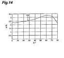
- the inventors performed elaborate research in order to accomplish the above object and found that, while it was common recognition of those skilled in the art that the energy conversion efficiency was effectively enhanced by incidence of light to the semiconductor electrode from the direction of the normal to the electrode surface (photoreceptive surface) (which will be referred to hereinafter as "normal incidence”), the dye-sensitized solar cells were able to demonstrate higher utilization factors of incident light and thus increase electric power generated per unit effective area, as compared with the normal incidence cells, when the light was made incident at angles of incidence in the range of 30 to 80° relative to the direction of the normal to the electrode surface (which will be referred to hereinafter as "oblique incidence").
- the light incidence angle dependence of energy conversion efficiency was measured with a dye-sensitized solar cell 100 (which has the structure similar to the dye-sensitized solar cell UC shown in Fig. 6), which had a photo-electrode in structure wherein a TiO 2 semiconductor electrode having the 50 mm 2 area of a portion contributing to power generation in the photoreceptive surface and the thickness of 20 ⁇ m was formed on a glass substrate having the thickness of 1.1 mm; an electrolyte consisting of an iodine base redox solution; and a counter electrode CE in structure wherein a thin film of Pt (film thickness; 3nm) was deposited on a fluorine-doped SnO 2 coated glass substrate having the shape and size similar to those of the foregoing glass substrate, and the results obtained are presented in the graph of Fig.
- ⁇ on the ordinate in Fig. 14 represents “effective energy conversion efficiency” described hereinafter. As apparent from the results presented in Fig. 14, it was verified that the energy conversion efficiency was enhanced by oblique incidence of light at angles of incidence in the range of 30 to 80° relative to the direction of the normal to the electrode surface.
- Fig. 15 (a) is a graph to show the current-voltage characteristics and energy conversion efficiency in the case where the light was made incident at the incidence angle of about 45° relative to the direction of the normal to the electrode surface of the dye-sensitized solar cell 100, and Fig.
- the resultant maximum energy conversion efficiency was 4.3140% (short-circuit current I sc ; 0.3030 mA, open-circuit voltage Voc; 0.6024 V, fill factor F.F.; 0.7289).
- the resultant maximum energy conversion efficiency was 3.7080% (short-circuit current I sc ; 0.2427 mA, open-circuit voltage Voc; 0.5880 V, fill factor F.F.; 0.8875).
- a dye-sensitized solar cell of the present invention is a dye-sensitized solar cell which comprises a photo-electrode having a semiconductor electrode and a transparent electrode placed on a photoreceptive surface of the semiconductor electrode, and a counter electrode and in which the semiconductor electrode is opposed through an electrolyte to the counter electrode, wherein the photoreceptive surface of the semiconductor electrode is formed so that an angle of incidence of light incident to the photoreceptive surface of the semiconductor electrode from a direction of a normal to a photoreceptive surface of the transparent electrode falls within a range of 30 to 80°.
- the sufficiently long optical paths can be secured in the semiconductor electrode without loss of the advantages that (1) optical excitation of the dye in the semiconductor electrode and injection of electrons into the semiconductor can be efficiently effected in the region near the transparent electrode with low electric resistance and low carrier loss and that (2) dye reduction, reaction in which redox species of I - /I 3 - or the like act on the dye as having optically been excited and injected electrons into the semiconductor, can be efficiently brought about in the region near the electrolyte with small ion diffusion resistance, in the case of the small thickness of the semiconductor electrode; it is, therefore, feasible to enhance the incident light harvest efficiency and, in turn, to enhance the energy conversion efficiency per unit effective area of the semiconductor electrode.
- the dye-sensitized solar cell of the present invention employing the oblique incidence is able to achieve the improvement of 5 to 50% in the energy conversion efficiency per unit effective area of the semiconductor electrode, as compared with the conventional dye-sensitized solar cells employing the normal incidence.
- the "effective area of the semiconductor electrode” in the present invention refers to an area represented by S 0 cos ⁇ , where S 0 is an actual area of the photoreceptive surface of the semiconductor electrode and ⁇ is an angle of incidence of light incident to the photoreceptive surface of the semiconductor electrode from the direction of the normal to the photoreceptive surface of the transparent electrode. Namely, when the photoreceptive surface of the semiconductor electrode is inclined at an inclination angle ⁇ relative to the photoreceptive surface of the transparent electrode or the installation surface where the dye-sensitized solar cell is installed, the effective area of the semiconductor electrode represents an area of an orthogonal projection of the actual area S 0 .
- the "energy conversion efficiency per unit effective area of the semiconductor electrode” will be referred to hereinafter as "effective energy conversion efficiency" in the following description.
- the first reason is that when the photoreceptive surface of the transparent electrode is parallel to the photoreceptive surface of the semiconductor electrode, reflection becomes noticeable on the surface of the transparent electrode at incident angles over 80° and the light becomes hard to arrive at the semiconductor electrode.
- the other reason is that when the light is incident normally to the transparent electrode and incident at the incident angles over 80° to the semiconductor electrode, the reflection loss and scattering loss increase at the interface between the transparent electrode and the semiconductor electrode.
- the angle of incidence of the light incident to the photoreceptive surface of the semiconductor electrode from the direction of the normal to the photoreceptive surface of the transparent electrode is more preferably in the range of 40 to 75° and still more preferably in the range of 50 to 70°.
- the thickness of the semiconductor electrode in the dye-sensitized solar cell of the present invention is preferably in the range of 5 to 30 ⁇ m, more preferably in the range of 5 to 15 ⁇ m, and still more preferably in the range of 8 to 13 ⁇ m.
- the thickness of the semiconductor electrode is less than 5 ⁇ m, the dye adsorption amount is small and the semiconductor electrode increases a tendency of failing to effectively absorb the light.
- the electric resistance increases to increase the amount of loss of carriers injected into the semiconductor, and the ion diffusion resistance also increases, so that injection of electrons from I - into the dye as having optically been excited and injected electrons into the semiconductor hinders transport of I 3 - to the counter electrode, thereby increasing a tendency of degrading the output characteristics of the cell.
- Another dye-sensitized solar cell of the present invention is a dye-sensitized solar cell which comprises a photo-electrode having a semiconductor electrode and a transparent electrode placed on a photoreceptive surface of the semiconductor electrode, and a counter electrode and in which the semiconductor electrode is opposed through an electrolyte to the counter electrode, wherein the transparent electrode is provided with lightguide means for changing a traveling direction of light incident from the outside to the photoreceptive surface of the transparent electrode so that an angle of incidence of the light traveling in the transparent electrode to enter the photoreceptive surface of the semiconductor electrode falls within a range of 30 to 80°.
- the lightguide means for changing the traveling direction of the light incident from the outside of the cell to the photoreceptive surface of the transparent electrode is provided in the upper part of the transparent electrode whereby the light incident normally to the photoreceptive surface of the transparent electrode is made obliquely incident to the photoreceptive surface of the semiconductor electrode, it becomes feasible to secure sufficiently long optical paths in the semiconductor electrode even under the small thickness condition of the semiconductor electrode, as in the case of the dye-sensitized solar cell described previously. For that reason, it becomes feasible to enhance the incident light harvest efficiency and, in turn, enhance the effective energy conversion efficiency.
- the "traveling direction of the light incident from the outside to thephotoreceptive surface of the transparent electrode,” which is a reference for formation of the photoreceptive surface of the transparent electrode or the photoreceptive surface of the semiconductor electrode, indicates the direction of the normal to the photoreceptive surface of the transparent electrode (e.g., cf. a surface F1 and a surface F2 shown in Fig. 4 described hereinafter) when the photoreceptive surface of the transparent electrode is flat.
- the "traveling direction” indicates the direction of the normal to the photoreceptive surface of the semiconductor electrode (e.g., cf. a surface F1 and a surface F2 shown in Fig. 3 described hereinafter).
- a flat, virtual plane is set as a virtual, photoreceptive surface inside the transparent electrode or the semiconductor electrode
- the traveling direction of the light incident from the outside is defined along a direction of a normal to the virtual, photoreceptive surface
- the actual photoreceptive surface of the transparent electrode or photoreceptive surface of the semiconductor electrode is designed on the basis of the reference of the traveling direction.
- the traveling direction of the incident light entering the semiconductor electrode can be controlled so as to avoid the collecting electrodes, whereby test cells on the laboratory level scale can be readily scaled up to cells on the practical use scale, without causing decrease of the effective energy conversion efficiency due to the collecting electrodes (comb-shaped electrodes).
- the dye-sensitized solar cell of the present invention has the structure provided with the lightguide means as described above and when the photoreceptive surface of the semiconductor electrode is flat, the aforementioned "effective area of the semiconductor electrode" is equal to the actual area S 0 . Accordingly, in the present invention, the "effective energy conversion efficiency" in the case of the solar cells in such structure is the energy conversion efficiency per S 0 , instead of S 0 cos ⁇ .
- the angle of incidence of the light incident to the photoreceptive surface of the semiconductor electrode from the direction of the normal to the photoreceptive surface of the transparent electrode or from the direction of the normal to the photoreceptive surface of the semiconductor electrode is also more preferably in the range of 40 to 75° and still more preferably in the range of 50 to 70°.
- the thickness of the semiconductor electrode is also preferably in the range of 5 to 30 ⁇ m, more preferably in the range of 5 to 15 ⁇ m, and still more preferably in the range of 8 to 13 ⁇ m.
- Another dye-sensitized solar cell of the present invention is a dye-sensitized solar cell which comprises a photo-electrode having a semiconductor electrode and a transparent electrode placed on a photoreceptive surface of the semiconductor electrode, and a counter electrode and in which the semiconductor electrode is opposed through an electrolyte to the counter electrode, wherein a plurality of collecting electrodes are provided on the photoreceptive surface of the semiconductor electrode, wherein the photoreceptive surface of the semiconductor electrode is formed so that an angle of incidence of light traveling in the transparent electrode to enter the photoreceptive surface of the semiconductor electrode falls within a range of 30 to 80°, and wherein a photoreceptive surface of the transparent electrode is formed so that the light selectively impinges on areas without the collecting electrodes on the photoreceptive surface of the semiconductor electrode.
- the "traveling direction of the light incident from the outside to the photoreceptive surface of the transparent electrode,” which is the reference for formation of the photoreceptive surface of the transparent electrode or the photoreceptive surface of the semiconductor electrode, also indicates the direction of the normal to the photoreceptive surface of the transparent electrode when the photoreceptive surface of the transparent electrode is flat.
- the "traveling direction” indicates the direction of the normal to the photoreceptive surface of the semiconductor electrode.
- a flat, virtual plane is set as a virtual, photoreceptive surface inside the transparent electrode or the semiconductor electrode
- the traveling direction of the light incident from the outside is defined along a direction of a normal to the virtual, photoreceptive surface
- the actual photoreceptive surface of the transparent electrode or photoreceptive surface of the semiconductor electrode is designed on the basis of the reference of the traveling direction (cf. a virtual, photoreceptive surface FP1 shown in Fig. 9 described hereinafter).
- the photoreceptive surface of the semiconductor electrode and the photoreceptive surface of the transparent electrode so as to satisfy the above condition, it becomes feasible to control the angle of incidence of the light incident to the electrode surface of the semiconductor electrode more precisely and readily.
- the traveling direction of the incident light entering the semiconductor electrode can be controlled so as to avoid the collecting electrodes, whereby the test cells on the laboratory level scale can be readily scaled up to the cells on the practical use scale, without causing decrease of the effective energy conversion efficiency due to the collecting electrodes (comb-shaped electrodes).
- the angle of incidence of the light incident to the photoreceptive surface of the semiconductor electrode is also more preferably in the range of 40 to 75° and still more preferably in the range of 50 to 70°.
- the thickness of the semiconductor electrode is also preferably in the range of 5 to 30 ⁇ m, more preferably in the range of 5 to 15 ⁇ m, and still more preferably in the range of 8 to 13 ⁇ m.
- a dye-sensitized solar cell module of the present invention is a dye-sensitized solar cell module comprising a plurality of dye-sensitized solar cells placed on a base, each dye-sensitized solar cell comprising a photo-electrode having a semiconductor electrode and a transparent electrode placed on a photoreceptive surface of the semiconductor electrode, and a counter electrode and in each dye-sensitized solar cell the semiconductor electrodebeing opposed through an electrolyte to the counter electrode, wherein each dye-sensitized solar cell is placed so that an angle of incidence of light incident to each dye-sensitized solar cell from a direction of a normal to an installation surface of the base falls within a range of 30 to 80°.
- the light reflected on the photoreceptive surface of the semiconductor electrode in one dye-sensitized solar cell can be made obliquely incident to the photoreceptive surface of the semiconductor electrode in another dye-sensitized solar cell, whereby a significant antireflection effect can be achieved as the entire module.
- the angle of incidence of the light incident to each dye-sensitizedsolar cell from the direction of the normal to the installation surface of the base is also more preferably in the range of 40 to 75° and still more preferably in the range of 50 to 70°.
- the thickness of the semiconductor electrode is also preferably in the range of 5 to 30 ⁇ m, more preferably in the range of 5 to 15 ⁇ m, and still more preferably in the range of 8 to 13 ⁇ m.
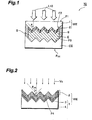
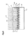
- Fig. 1 is a schematic, sectional view showing the first embodiment of the dye-sensitized solar cell according to the present invention.
- the dye-sensitized solar cell 10 of the present embodiment is mainly comprised of a photo-electrode WE having a semiconductor electrode 2 with the thickness of 5 to 30 ⁇ m and a transparent electrode 1 placed on a photoreceptive surface F2 of the semiconductor electrode 2, a counter electrode CE, and an electrolyte E filled in a space formed between the photo-electrode WE and the counter electrode CE by spacer S.
- this dye-sensitized solar cell 10 light L10 passing through the transparent electrode 1 to impinge on the semiconductor electrode 2 generates electrons in the semiconductor electrode 2. Then the electrons generated in the semiconductor electrode 2 are collected to the transparent electrode 1 and taken out to the outside.
- the semiconductor electrode 2 is formed so that the angle ⁇ of incidence of the light L10 incident to the photoreceptive surface F2 of the semiconductor electrode from the direction of the normal to the photoreceptive surface F1 of the transparent electrode 1 falls within the range of 30 to 80°. Namely, when the semiconductor electrode 2 is viewed from the direction of the cross section thereof, the electrode layer is formed in sawtooth shape. The contact surface of the transparent electrode 1 with the semiconductor electrode 2 is also grooved in sawtooth shape fitting the shape of the semiconductor electrode 2.
- the counter electrode CE is also grooved in sawtooth shape in agreement with the shape of the semiconductor electrode 2, in a surface F3 thereof in contact with the electrolyte E.
- the period of the sawtooth projections and depressions is approximately several millimeters and the gap between the photo-electrode WE and the counter electrode CE is approximately 50 to 100 ⁇ m in Fig. 1. Therefore, the dye-sensitized solar cell 10 of Fig. 1 is emphatically illustrated as expanded in the vertical direction (or in the traveling direction of the light L10).
- the surface F3 of the counter electrode CE is made in the sawtooth shape in agreement with the shape of the semiconductor electrode 2 whereby the counter electrode CE and the photo-electrode WE are arranged in parallel with each other with the layer of electrolyte E in between and thus can create a uniform, parallel electric field between them. If the shape of the surface F3 of the counter electrode CE on the electrolyte E side should be flat, the electric field would be concentrated at the projections on the photo-electrode side, so as to impede stable operation.
- the transparent electrode can be one obtained by coating a semiconductor-electrode-side surface of a transparent substrate such as a glass substrate or the like (not shown) with a so-called transparent, conductive film transmitting light (cf. Fig. 2) and is, for example, a fluorine-doped SnO 2 coatad glass substrate, an ITO coated glass substrate, a ZnO:Al coated glass substrate, or the like.
- the semiconductor can be either one selected from oxide semiconductors, sulfide semiconductors, and so on.
- oxide semiconductors include, for example, TiO 2 , ZnO, SnO 2 , Nb 2 O 5 , In 2 O 3 , WO 3 , ZrO 2 , La 2 O 3 , Ta 2 O 5 , SrTiO 3 , BaTiO 3 , and so on.
- sulfide semiconductors include, for example, CdS and others.
- Si, GaAs, and so on there are no specific restrictions on the dye included in the semiconductor electrode 2, and the dye can be, for example, either one selected from ruthenium complexes, metal phthalocyanine, and so on.
- the counter electrode CE may be one wherein a thin-film metal electrode of Pt or the like is formed on a transparent, conductive film, similar to the aforementioned transparent electrode 1, and wherein the thin-film metal electrode is placed on the electrolyte E side.
- the composition of the electrolyte E either, as long as it contains the redox species for reducing the dye as having optically been excited to inject electrons into the semiconductor.
- a preferred electrolyte is an iodine base redox solution containing the redox species of I - /I 3 - or the like.
- the constitutive material of the spacer S either, and it can be, for example, silica beads or the like.
- Fig. 2 shows an example of a step of producing the photo-electrode WE in the dye-sensitized solar cell 10 of Fig. 1.
- the transparent electrode 1 can be made by a known method, e.g., a method of depositing a transparent, conductive film 3 of fluorine-doped SnO 2 or the like, described previously, on a substrate 4 such as a glass substrate or the like by spray coating.
- the shape of the surface F4 of the substrate 4 on which the transparent, conductive film 3 is deposited is formed in the sawtooth cross section so as to match with the value of the angle ⁇ of incidence of the light incident to the photoreceptive surface F2 of the complete semiconductor electrode 2.
- the surface of the substrate 4 may be shaped, for example, by matching the shape of a mold, used for formation of the substrate 4 by casting, with the sawtooth section shape or by cutting one surface of the substrate formed in an approximately rectangular parallelepiped shape, into the aforementioned shape.
- the semiconductor electrode 2 is formed by depositing a film of a semiconductor Vs of TiO 2 or the like on the transparent, conductive film 3 of the transparent electrode 1, as shown in Fig. 2.
- a method of depositing the film of the semiconductor on the transparent, conductive film 3 can be either one of known methods.
- applicable known methods include physical evaporation methods such as electron beam evaporation, resistive heating evaporation, sputter evaporation, ionized cluster beam evaporation, and so on, and a reactive evaporation method in which a metal or the like is evaporated in reactive gas of oxygen or the like to deposit a reaction product on the transparent, conductive film 3.
- an angle ⁇ vs of incidence of evaporative particles relative to the direction of the normal to the surface F4 of the substrate 4 on the side where the transparent, conductive film 3 is formed is preferably in the range of 30° to 80° and is more preferably a value equal to the angle ⁇ of incidence described previously.
- the electrode layer (deposited film) of the semiconductor formed on the transparent, conductive film 3 on the surface F4 is formed in the structure wherein deposited semiconductor particles form a plurality of adjacent, columnar aggregates having the slope in the range of 15 to 40° relative to the direction of the normal to the photoreceptive surface F4.
- the electrode layer of the semiconductor having this columnar structure has a larger surface area and can contain an increased amount of the dye when compared with the electrode layer of the semiconductor formed by deposition of evaporated particles from the direction of the normal to the photoreceptive surface F4, it becomes feasible to enhance the cell output and the energy conversion efficiency. If the angle ⁇ vs of incidence of the evaporative particles is less than 30°, the self-shielding effect in the evaporation becomes unnoticeable and it tends to become hard to form the definite columnar structure. When the angle ⁇ vs of incidence of the evaporative particles exceeds 80° on the other hand, the film becomes of very coarse structure and the mechanical strength could be reduced over the permissible range of practical use.
- the method may be selected from a method of preliminarily placing the substrate 4 at the predetermined angle relative to the traveling direction of the evaporative particles in an evaporation system, a method of quickly moving the substrate 4 relative to an evaporation source, and a method of providing two evaporation sources and simultaneously depositing the evaporative particles in two directions of incidence thereof to the surface F4.
- the semiconductor deposited film may be subjected to a thermal treatment under a predetermined temperature condition according to necessity, to cause phase transition thereof.
- a thermal treatment crystallizes the amorphous semiconductor film into the anatase phase. This results in forming a clear band structure by crystallization, growing crystalline particles of the semiconductor, improving bonding between crystalline particles in conjunction therewith, and so on to enhance the injection efficiency of electrons from the dye into the semiconductor or facilitate migration of electrons in the semiconductor deposited film, thereby further enhancing the energy conversion efficiency.
- the semiconductor deposited film can be provided with many oxygen defects, so as to increase the electric conductivity of the semiconductor deposited film, thereby further enhancing the energy conversion efficiency.
- the semiconductor deposited film is impregnated with the dye by a known method such as an immersion method or the like, thereby completing the semiconductor electrode 2.
- the deposited film may be impregnated with a metal such as silver or the like or a metal oxide such as alumina or the like according to necessity, in addition to the dye.
- the counter electrode CE is made by a known method and the counter electrode, photo-electrode WE, and the spacer S are assembled as shown in Fig. 1. Then the interior is filled with the electrolyte E to complete the dye-sensitized solar cell 10.
- Fig. 3 is a schematic, sectional view showing the second embodiment of the dye-sensitized solar cell according to the present invention.
- the dye-sensitized solar cell 11 of the present embodiment is mainly comprised of the photo-electrode WE having the semiconductor electrode 2 with the thickness of 5 to 30 ⁇ m and the transparent electrode 1 placed on the photoreceptive surface F2 of the semiconductor electrode 2, the counter electrode CE, and the electrolyte E filled in the space formed between the photo-electrode WE and the counter electrode CE by the spacer S.
- This dye-sensitized solar cell 11 has substantially the same structure as the conventional dye-sensitized solar cells, except for an optical waveguide layer 5 (lightguide means) provided on the photoreceptive surface side of the transparent electrode 1.
- the optical waveguide layer 5 has a function of changing the traveling direction of the light L11 so that the angle ⁇ of incidence of the light L11 incident to the photoreceptive surface F2 of the semiconductor electrode 2 from the direction of the normal to the photoreceptive surface F2 of the semiconductor electrode 2 falls within the range of 30 to 80°.
- This optical waveguide layer 5 is comprised of a plurality of glass fibers 52 surfaces of which are plated with Ag and each of which has the diameter of about 1 mm. When each glass fiber 52 is placed on the photoreceptive surface F1 of the transparent electrode 1, it is arranged to be inclined (at an angle ⁇ 5 of inclination) relative to the direction of the normal to the photoreceptive surface F2 of the semiconductor electrode 2.
- each glass fiber 52 of the optical waveguide layer 5 is adjusted so as to agree with the angle ⁇ of incidence of the light L11 obliquely incident to the photoreceptive surface F2 of the semiconductor electrode 2.
- the light L11 coming from the direction of the normal to the photoreceptive surface F1 of the transparent electrode 1 into the optical waveguide layer 5 enters each glass fiber 52 of the optical waveguide layer 5, it changes its traveling direction to be controlled so that the angle of incidence thereof falls within the range of 30 to 80° upon incidence to the photoreceptive surface F2 of the semiconductor electrode 2.
- the glass fibers 52 constituting the optical waveguide layer 5 can be made, for example, byplating the surfaces with Ag by a known method, thereafter bundling and securing them, and obliquely cutting them crosswise so as to achieve the aforementioned inclination angle.
- This optical waveguide layer 5 may be one also serving as a protective glass layer provided on the photoreceptive surface F1 of the transparent electrode 1.
- the optical waveguide layer 5 may be doped with a rare earth element to be provided with fluorescence to ultraviolet light. Further, it is also possible to provide a separate, protective glass layer (not shown) from the optical waveguide layer 5 and in this case, the protective glass layer is not laid on the photoreceptive surface F1 of the transparent electrode 1, but laid on the optical waveguide layer 5.
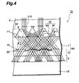
- Fig. 4 is a schematic, sectional view showing the third embodiment of the dye-sensitized solar cell according to the present invention.
- the dye-sensitized solar cell 12 of the present embodiment is mainly comprised of the photo-electrode WE having the semiconductor electrode 2 with the thickness of 5 to 30 ⁇ m and the transparent electrode 1 placed on the photoreceptive surface F2 of the semiconductor electrode 2, the counter electrode CE, and the electrolyte E filled in the space formed between the photo-electrode WE and the counter electrode CE by the spacer S (not shown).
- This dye-sensitized solar cell 12 has substantially the same structure as the dye-sensitized solar cell 11 shown in Fig. 3, except that the optical waveguide layer 5 (lightguide means) of shape different from that of the dye-sensitized solar cell 11 shown in Fig. 3 is provided on the photoreceptive surface side of the transparent electrode 1 and that there are comb-shaped electrodes (collecting electrodes) 22 provided on the photoreceptive surface F2 side of the semiconductor electrode 2, for provision for a scaleup of unit cells of dye-sensitized solar cells to the practical use scale.
- the optical waveguide layer 5 of the dye-sensitized solar cell 12 is a layer wherein a plurality of grooves (of a substantially trapezoid cross section) are formed in parallel arrangement in a surface on the photoreceptive surface F1 side of the transparent electrode 1 whereby a plurality of projections 53 having a substantially triangular cross section are formed between the grooves.
- Each projection 53 has reflective facets F5 for changing the traveling direction of the light traveling in the optical waveguide layer 5.
- the optical waveguide layer 5 is placed on the transparent electrode 1 so that the tips of the projections 53 are in contact with the photoreceptive surface F1 of the transparent electrode 1. This results in forming the photoreceptive facets F5 having predetermined inclination angles relative to the photoreceptive surface F1 of the transparent electrode 1, in the optical waveguide layer 5.
- Each reflective facet F5 is comprised of a reflective face R1 having the inclination angle of ⁇ 3 relative to the photoreceptive surface F1 of the transparent electrode 1 and formed in a lower local area and a reflective face R2 having the inclination angle of ⁇ 4 (> ⁇ 3) relative to the photoreceptive surface F1 of the transparent electrode 1 and formed in an upper local area.
- spaces 6 of the substantially trapezoid cross section are formed between the optical waveguide layer 5 and the transparent electrode 1 because of the geometry of the optical waveguide layer 5.
- the spaces 6 are preferably kept in a vacuum state or filled with gas such as air or the like from a viewpoint of total reflection, but they may be filled, for example, with an organic material or the like if the refractive index thereof satisfies the condition of 86.6% or less of the refractive index of the optical waveguide layer 5.
- faces F55 of the optical waveguide layer 5 corresponding to upper base portions of the trapezoid cross section of the spaces 6 shown in Fig. 4 are provided for the reason of machining and areas of these portions are preferably as small as possible. Accordingly, it is more preferable that the spaces 6 formed between the optical waveguide layer 5 and the transparent electrode 1 be ideally of a substantially triangular cross section.
- the light L12 incident to the reflective facets F5 of the optical waveguide layer 5 from the direction of the normal to the photoreceptive surface F1 of the transparent electrode 1 is controlled in its traveling direction so that the angle ⁇ of incidence of each beam to the photoreceptive surface F2 of the semiconductor electrode 2 falls within the range of 30 to 80° so as to avoid the comb-shaped electrodes 22 by making use of the difference between the inclination angles of the reflective face R1 formed in the lower local area and the reflective face R2 formed in the upper local area. Since in the dye-sensitized solar cell 12 the angles ⁇ of incidence of the beams incident to the photoreceptive surface F2 of the semiconductor electrode 2 are not uniform, Fig. 4 shows only the incident angle ⁇ 1 as an example of the incident angles ⁇ .
- the dye-sensitized solar cell 12 to avoid the degradation of the energy conversion efficiency due to the comb-shaped electrodes 22, as used to occur in the conventional dye-sensitized solar cells, even if the cell is scaled up to the practical use scale (e.g., 100 ⁇ 100 mm); therefore, it can enhance the incident light harvest efficiency and the effective energy conversion efficiency, as in the case of the dye-sensitized solar cell 10 shown in Fig. 1 and the dye-sensitized solar cell 11 shown in Fig. 3.
- the practical use scale e.g. 100 ⁇ 100 mm
- the refractive index of the portions of the spaces 6 shown in Fig, 4 is typically 86.6% or less of the refractive index of the optical waveguide layer 5.
- the refractive index of the transparent electrode 1 is preferably larger than the refractive index of the portions of the spaces 6 shown in Fig. 4.
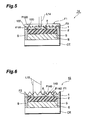
- Fig. 5 is a schematic, sectional view showing the fourth embodiment of the dye-sensitized solar cell according to the present invention.
- the dye-sensitized solar cell 14 of the present embodiment is mainly comprised of the photo-electrode WE having the semiconductor electrode 2 with the thickness of 5 to 30 ⁇ m and the transparent electrode 1 placed on the photoreceptive surface F2 of the semiconductor electrode 2, the counter electrode CE, and the electrolyte E filled in the space formed between the photo-electrode WE and the counter electrode CE by the spacer S.
- This dye-sensitized solar cell. 14 has substantially the same structure as the dye-sensitized solar cell 11 shown in Fig. 3, except that there is provided the transparent electrode 1 (lightguide means) having the structure different from that of the dye-sensitized solar cell 11 shown in Fig. 3 and that the optical waveguide layer 5 is not provided.
- the lightguide means of the dye-sensitized solar cell 14 is a plurality of reflective portions 120 formed in the transparent electrode 1.
- Each reflective portion 120 consists of reflective facets F120 for changing the traveling direction of the light L14 traveling in the transparent electrode 1.
- the interior of each reflective portion 120 is a space 122 of a substantially triangular cross section.
- This space 122 is preferably kept in a vacuum state or filled with gas such as air or the like from the viewpoint of the total reflection, but the space may be filled, for example, with an organic material or the like as long as the refractive index thereof satisfies the condition of 86.6% or less of the refractive index of the transparent electrode 1.
- the reflective facets F120 of the respective reflective portions 120 are formed with a predetermined inclination (an inclination angle ⁇ 120) relative to the direction of the normal to the photoreceptive surface F2 of the semiconductor electrode 2 so that the angle ⁇ of incidence of the light incident to the photoreceptive surface F2 of the semiconductor electrode 2 falls within the range of 30 to 80°.
- This also permits the dye-sensitized solar cell 14 to enhance the incident light harvest efficiency and the effective energy conversion efficiency, as in the case of the aforementioned dye-sensitized solar cell 10, dye-sensitized solar cell 11, and dye-sensitized solar cell 12.
- the refractive index of the portions of the spaces 122 shown in Fig. 5 needs to be 86.6% or less of the refractive index of the transparent electrode 1.
- Fig. 6 is a schematic, sectional view showing the fifth embodiment of the dye-sensitized solar cell according to the present invention.
- the dye-sensitized solar cell 15 of the present embodiment is mainly comprised of the photo-electrode WE having the semiconductor electrode 2 with the thickness of 5 to 30 ⁇ m and the transparent electrode 1 placed on the photoreceptive surface F2 of the semiconductor electrode 2, the counter electrode CE, and the electrolyte E filled in the space formed between the photo-electrode WE and the counter electrode CE by the spacer S.
- This dye-sensitized solar cell 15 has substantially the same structure as the dye-sensitized solar cell 11 shown in Fig. 3, except that there is provided the transparent electrode 1 (lightguide means) having the structure different from that of the dye-sensitized solar cell 11 shown in Fig. 3 and that the optical waveguide layer 5 is not provided.
- the lightguide means of the dye-sensitized solar cell 15 is a plurality of projections 140 formed on the photoreceptive surface F1 of the transparent electrode 1.
- Each projection 140 has reflective facets F140 for changing the traveling direction of the light L15 incident from the direction of the normal to the photoreceptive surface F2 of the semiconductor electrode 2.
- the reflective facets F140 of the respective projections 140 are formed with a predetermined inclination (an inclination angle ⁇ 140) relative to the direction of the normal to the photoreceptive surface F2 of the semiconductor electrode 2 so that the angle ⁇ of incidence of the light incident to the photoreceptive surface F2 of the semiconductor electrode 2 falls within the range of 30 to 80°.
- This also permits the dye-sensitized solar cell 15 to enhance the incident light harvest efficiency and the effective energy conversion efficiency, as in the case of the foregoing dye-sensitized solar cell 10, dye-sensitized solar cell 11, dye-sensitized solar cell 12, and dye-sensitized solar cell 14.
- the refractive index of the transparent electrode 1 needs to be larger than that of air but smaller than that of the semiconductor electrode 2.
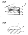
- Fig. 7 is a schematic, sectional view showing the fifth embodiment of the dye-sensitized solar cell according to the present invention.
- Fig. 8 is an enlarged view of a region R shown in Fig. 7.
- the dye-sensitized solar cell 16 of the present embodiment is mainly comprised of the photo-electrode WE having the semiconductor electrode 2 with the thickness of 5 to 30 ⁇ m and the transparent electrode 1 placed on the photoreceptive surface F2 of the semiconductor electrode 2, the counter electrode CE, and the electrolyte E filled in the space formed between the photo-electrode WE and the counter electrode CE by the spacer S.
- This dye-sensitized solar cell 16 has substantially the same structure as the dye-sensitized solar cell 11 shown in Fig. 3, except that there is provided the transparent electrode 1 (lightguide means) having the structure different from that of the dye-sensitized solar cell 11 shown in Fig. 3 and that the optical waveguide layer 5 is not provided.
- the lightguide means of the dye-sensitized solar cell 16 is a plurality of diffraction grating stripes 160 formed on the photoreceptive surface F1 of the transparent electrode 1.
- the diffraction grating stripes 160 are made of a transparent material having a refractive index higher than that of the transparent electrode 1 and are adapted to diffract the light L16 incident from the direction of the normal to the photoreceptive surface F2 of the semiconductor electrode 2, at predetermined angles so that angles of incidence of beams incident to the photoreceptive surface F2 of the semiconductor electrode 2 fall within the range of 30 to 80°.
- the transparent material having the refractive index higher than that of the transparent electrode 1 can be selected, for example, from Ta 2 O 5 and others.
- Fig. 7 shows a state in which the first-order diffracted light L161 and the second-order diffracted light L162 of the light L16 incident from the direction of the normal to the photoreceptive surface F2 of the semiconductor electrode 2 is incident at the incidence angles ⁇ 161 and ⁇ 162, respectively, in the range of 30 to 80° relative to the photoreceptive surface F2 of the semiconductor electrode 2.
- the dye-sensitized solar cell 16 to enhance the incident light harvest efficiency and the effective energy conversion efficiency, as in the case of the foregoing dye-sensitized solar cell 10, dye-sensitized solar cell 11, dye-sensitized solar cell 12, dye-sensitized solar cell 14, and dye-sensitized solar cell 15.
- the transparent material as a constitutive material of the diffraction grating stripes 160 is preferably a material having the refractive index of not less than 2.0.
- Fig. 9 is a schematic, sectional view showing the seventh embodiment of the dye-sensitized solar cell according to the present invention.
- the dye-sensitized solar cell 17 of the present embodiment is mainly comprised of the photo-electrode WE having the semiconductor electrode 2 with the thickness of 5 to 30 ⁇ m and the transparent electrode 1 placed on the photoreceptive surface F2 of the semiconductor electrode 2, the counter electrode CE, and the electrolyte E filled in the space formed between the photo-electrode WE and the counter electrode CE by the spacer S.
- the dye-sensitized solar cell 17 has substantially the same structure as the dye-sensitized solar cell 10 shown in Fig. 1, except that there is provided the transparent electrode 1 of shape different from that of the dye-sensitized solar cell 10 shown in Fig. 1 and that there are provided the comb-shaped electrodes (collecting electrodes) 22 on the photoreceptive surface F2 side of the semiconductor electrode 2, for provision for a scaleup of unit cells of dye-sensitized solar cells to the practical use scale.
- the photoreceptive surface F2 of the semiconductor electrode 2 is formed so that angles ⁇ of incidence of the light traveling in the transparent electrode 1 to enter the photoreceptive surface F2 of the semiconductor electrode 2 fall within the range of 30 to 80° and the photoreceptive surface F1 of the transparent electrode 1 is formed so that the light selectively impinges on areas without the collecting electrodes 22 on the photoreceptive surface F2 of the semiconductor electrode 2.
- the semiconductor electrode 2 shown in Fig. 9 is formed so that the electrode layer is of the sawtooth shape when viewed from the sectional direction.
- the contact surface of the transparent electrode 1 with the semiconductor electrode 2, shown in Fig. 9 is also provided with grooves in the sawtooth shape in agreement with the shape of the semiconductor electrode 2.
- the photoreceptive surface F1 of the transparent electrode 1 shown in Fig. 9 has a plurality of projections 170 of convex lens shape. The radius of curvature of each projection 170 is set so that the light selectively impinges on the areas without the collecting electrodes 22 on the photoreceptive surface F2 of the semiconductor electrode 2.
- a virtual, flat plane is set as a virtual, photoreceptive surface FP1 inside the transparent electrode 1 or the semiconductor electrode 2.
- the traveling direction of the light incident from the outside is defined along the direction of the normal to the virtual, photoreceptive surface FP1, and the actual photoreceptive surface F1 of the transparent electrode 1 or photoreceptive surface F2 of the semiconductor electrode 2 is designed on the basis of the reference of the traveling direction.
- the present embodiment shows an example in which the virtual, photoreceptive surface FP1 is set inside the transparent electrode 1.
- the dye-sensitized solar cell 17 to enhance the incident light harvest efficiency and the effective energy conversion efficiency, as in the case of the foregoing dye-sensitized solar cell 10, dye-sensitized solar cell 11, dye-sensitized solar cell 12, and dye-sensitized solar cell 14.
- the refractive index of the transparent electrode 1 is preferably not less than 1.4.
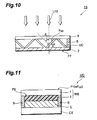
- Fig. 10 is a schematic, sectional view showing a preferred embodiment of the dye-sensitized solar cell module according to the present invention
- Fig. 11 a schematic, sectional view of one of the dye-sensitized solar cells composing the dye-sensitized solar cell module shown Fig. 10.
- the dye-sensitized solar cell module 13 of the present embodiment is mainly comprised of a plurality of dye-sensitized solar cells UC, a base 7 for the plurality of dye-sensitized solar cells UC to be mounted thereon, a spacer S, and a tempered glass sheet 9. As shown in Fig. 10, the dye-sensitized solar cell module 13 of the present embodiment is mainly comprised of a plurality of dye-sensitized solar cells UC, a base 7 for the plurality of dye-sensitized solar cells UC to be mounted thereon, a spacer S, and a tempered glass sheet 9. As shown in Fig.
- each dye-sensitized solar cell UC has substantially the same structure as the conventional cells and is mainly comprised of the photo-electrode WE having the semiconductor electrode 2 with the thickness of 5 to 30 ⁇ m and the transparent electrode 1 formed on the photoreceptive surface F2 of the semiconductor electrode 2, the counter electrode CE, and the electrolyte E filled in the space formed between the photo-electrode WE and the counter electrode CE by the spacer S.
- Each dye-sensitized solar cell UC is mounted on the base 7 so that the angle ⁇ of incidence of the light incident to the photoreceptive surface F UC of the cell from the direction of the normal to the installation surface F7 of the base 7 falls within the range of 30 to 80°. This enhances the incident light harvest efficiency of each dye-sensitized solar cell UC, whereby the effective energy conversion efficiency of the entire module can be enhanced as compared with the conventional dye-sensitized solar cell modules.
- the light source was the sunlight in the case of the dye-sensitized solar cells and dye-sensitized solar cell module in the above embodiments of the present invention, but the dye-sensitized solar cells and dye-sensitized solar cell modules of the present invention are not limited to this example; for example, the light source may be ultraviolet light.
- the light source may be ultraviolet light.
- the dye-sensitized solar cells and dye-sensitized solar cell modules of the present invention will be described below in further detail with examples and comparative examples, but it is noted that the present invention is by no means intended to be limited to these examples.
- the components of the dye-sensitized solar cells and dye-sensitized solar cell modules in the examples and comparative examples below will be described by using the same reference symbols for the same or equivalent portions as in the foregoing embodiments.
- the "effective energy conversion efficiency” indicates the energy conversion efficiency per S 0 instead of S 0 cos ⁇ , as described previously. Accordingly, "-" is given in the column of S 0 cos ⁇ in Table 1.
- the dye-sensitized solar cell on the scale of 50 ⁇ 50 mm with the same structure as the dye-sensitized solar cell 10 shown in Fig. 1 was fabricated as described below.
- TiO 2 was deposited from the direction described in the previous description of the dye-sensitized solar cell 10, onto the sawtooth surface of the transparent electrode 1 by electron beam evaporation to form the semiconductor electrode 2 having the actual area of the photoreceptive surface F2; 140 ⁇ 48 mm, the layer thickness; 7 ⁇ m, the length of one side of the sawtooth portion of the layer; 5 mm, and the angle ⁇ s of inclination of the sawtooth portion; 70° (the angle ⁇ of incidence of light to the photoreceptive surface F2; 70°).
- the evaporation system used herein was the BV-6D high vacuum evaporation system available from ULVAC JAPAN, Ltd.
- the evaporation source was TiO 2 (rutile, purity; 99.99%) available from Kojundo Chemical Laboratory Co., Ltd.
- the deposition conditions were the effective size of the evaporation surface; 47.9 ⁇ 48.0 mm, the evaporation speed; 1.4nm/s, the substrate temperature; 205°C, the degree of vacuum in the chamber of the evaporation system before the start of evaporation; 1 ⁇ 10 -3 Pa, and the degree of vacuum in the chamber of the evaporation system during the evaporation; 1 ⁇ 10 -3 Pa.
- the temperature of the sample holder of the evaporation system was increased at the increase rate of 10°C/min from 60°C to 400°C and the sample holder was retained at this temperature for 30 minutes to anneal the semiconductor electrode 2 of TiO 2 deposited on the transparent electrode 1.
- This annealing treatment crystallized the amorphous phase of TiO 2 deposited on the transparent electrode 1, into the anatase phase. It was preliminarily confirmed by X-ray diffraction that the amorphous phase of deposited TiO 2 was crystallized into the anatase phase by the foregoing annealing treatment.
- the dye was made to adsorb on the surface of the semiconductor electrode 2 of produced TiO 2 in the following manner.
- a ruthenium complex [cis-Di (thiocyanato) -N, N'-bis(2, 2'-bipyridyl-4, 4' dicarboxylic acid) -ruthenium(II)] was dissolved in the concentration of 2.85 ⁇ 10 -4 mol/L into a solvent of absolute ethanol dehydrated with magnesium ethoxide, thereby preparing a ruthenium complex solution.
- the semiconductor electrode 2 was immersed in this solution for twenty four hours.
- This operation made the semiconductor electrode 2 adsorb the ruthenium complex in about 1.0 ⁇ 10 -7 mol/cm 2 , which would become the dye. Then, in order to increase the open-circuit voltage Voc, the semiconductor electrode 2 after the adsorption of the ruthenium complex was immersed in an acetonitrile solution for fifteen minutes, and thereafter dried in a nitrogen stream kept at 25°C, thus completing the photo-electrode WE.
- the counter electrode CE was an electrode obtained by depositing a thin film of Pt (thickness; 3 nm) on a fluorine-doped SnO 2 coated glass substrate having the shape and size similar to those of the transparent electrode 1.
- the electrolyte E was an iodine base redox solution prepared in such a way that tetra-n-propylammonium iodide; 3.13 g and iodine; 0.18 g were dissolved in a mixed solution of ethylene carbonate; 21.14 g and acetonitrile; 4.0 mL. Further prepared was the spacer S (trade name: "Himilan”) available from DuPont Co.
- the substantially same dye-sensitized solar cell as in Example 1 was produced by the substantially same process as in Example 1, except that the semiconductor electrode 2 was prepared with the sawtooth portion at the inclination angle ⁇ s; 45° (the angle ⁇ of incidence of light to the photoreceptive surface F2; 45°).
- the substantially same dye-sensitized solar cell as in Example 1 was produced by the substantially same process as in Example 1, except that the semiconductor electrode 2 was prepared with the sawtooth portion at the inclination angle ⁇ s; 30° (the angle ⁇ of incidence of light to the photoreceptive surface F2; 30°).
- the substantially same dye-sensitized solar cell as in Example 1 was produced by the substantially same process as in Example 1, except that the shape of the photo-electrode WE and the counter electrode CE was the same as that in the conventional dye-sensitized solar cell shown in Fig. 11 (the angle of incidence of light to the photoreceptive surface F2; 0°).
- the substantially same dye-sensitized solar cell as in Example 1 was produced by the substantially same process as in Example 1, except that the semiconductor electrode 2 was prepared with the sawtooth portion at the inclination angle ⁇ s; 20° (the angle ⁇ of incidence of light to the photoreceptive surface F2; 20°).
- This dye-sensitized solar cell was produced in the structure in which among the components except for the optical waveguide layer 5 (the inclination angle ⁇ 5 relative to the photoreceptive surface F1 of the transparent electrode 1; 70° and the angle ⁇ of incidence of light to the photoreceptive surface F2; 70°) provided on the photoreceptive surface F1 of the transparent electrode 1, the shape of the photo-electrode WE and the counter electrode CE was similar to that in the conventional dye-sensitized solar cell shown in Fig. 11, and by the substantially same process as in Example 1.
- the glass fibers constituting the optical waveguide layer 5 were glass fibers having the diameter of 1 mm.
- the surfaces of the glass fibers were plated with Ag, they were bundled and secured, and thereafter they were obliquely cut crosswise in accordance with the aforementioned inclination angle ⁇ into the length of 5 mm.
- the glass fibers prepared in this way were mounted on the photoreceptive surface of the transparent electrode 1 with a glass adhesive.
- the substantially same dye-sensitized solar cell as in Example 4 was produced by the substantially same process as in Example 4, except that the optical waveguide layer 5 was prepared with the inclination angle ⁇ 5 to the photoreceptive surface F1 of the transparent electrode 1; 45° and the angle ⁇ of incidence of light to the photoreceptive surface F2; 45°.
- the substantially same dye-sensitized solar cell as in Example 4 was produced by the substantially same process as in Example 4, except that the optical waveguide layer 5 was prepared with the inclination angle ⁇ 5 to the photoreceptive surface F1 of the transparent electrode 1; 30° and the angle ⁇ of incidence of light to the photoreceptive surface F2; 30°.
- the dye-sensitized solar cell having the substantially same structure as in Example 4 was produced by the substantially same process as in Example 4, except that the optical waveguide layer 5 was doped with 0.2 mol% of a rare earth element (samarium) to enhance the fluorescence to ultraviolet light.
- a rare earth element samarium
- the dye-sensitized solar cell having the substantially same structure as in Comparative Example 1 was produced by the substantially same process as in Example 1, except that the rare earth element (samarium) was added 0.2 mol% near the photoreceptive surface F1 of the transparent electrode 1 in the dye-sensitized solar cell of Comparative Example 1.
- the rare earth element samarium
- Produced was the dye-sensitized solar cell having the substantially same structure as in Example 4, except that the semiconductor electrode having the thickness of 20 ⁇ m and the actual area S 0 of the photoreceptive surface; 73.47 mm 2 was formed on the transparent electrode 1 by screen-printing commercially available TiO 2 particles (average particle size; 30nm) and a paste prepared for screen printing with a screen printer and thereafter performing the thermal treatment under the temperature condition of 400°C for thirty minutes.
- Produced was the dye-sensitized solar cell having the substantially same structure as in Example 5, except that the semiconductor electrode having the thickness of 20 ⁇ m and the actual area S 0 of the photoreceptive surface; 73.47 mm 2 was formed on the transparent electrode 1 by screen-printing the commercially available TiO 2 particles (average particle size; 30 nm) and the paste prepared for screen printing with the screen printer and thereafter performing the thermal treatment under the temperature condition of 400°C for thirty minutes.
- Produced was the dye-sensitized solar cell having the substantially same structure as in Example 6, except that the semiconductor electrode having the thickness of 20 ⁇ m and the actual area S 0 of the photoreceptive surface; 73.47 mm 2 was formed on the transparent electrode 1 by screen-printing the commercially available TiO 2 particles (average particle size; 30 nm) and the paste prepared for screen printing with the screen printer and thereafter performing the thermal treatment under the temperature condition of 400°C for thirty minutes.
- the substantially same dye-sensitized solar cell as in Example 8 was produced by the substantially same process as in Example 8, except that the optical waveguide layer 5 was prepared with the inclination angle ⁇ 5 to the photoreceptive surface F1 of the transparent electrode 1; 0° and the angle ⁇ of incidence of light to the photoreceptive surface F2; 0°.
- the substantially same dye-sensitized solar cell as in Example 9 was produced by the substantially same process as in Example 9, except that the optical waveguide layer 5 was prepared with the inclination angle ⁇ 5 to the photoreceptive surface F1 of the transparent electrode 1; 20° and the angle ⁇ of incidence of light to the photoreceptive surface F2; 20°.
- the substantially same dye-sensitized solar cell as in Example 10 was produced by the substantially same process as in Example 10, except that the optical waveguide layer 5 was prepared with the inclination angle ⁇ 5 to the photoreceptive surface F1 of the transparent electrode 1; 85° and the angle ⁇ of incidence of light to the photoreceptive surface F2; 85°.
- the dye-sensitized solar cell having the substantially same structure as in Example 4 was produced by the substantially same process as in Example 4, except that the semiconductor electrode having the thickness of 10 ⁇ m and the actual area S 0 of the photoreceptive surface; 71.1 mm 2 was formed on the transparent electrode 1 by tape casting of two types of TiO 2 particles (average particle sizes; 200 nm and 25 nm) commercially available.
- the foregoing tape casting of TiO 2 particles was conducted according to the following procedure. Namely, powder of TiO 2 particles was first kneaded together with deionized water and a chelating agent in an alumina mortar. Then deionized water and a surfactant were added into the alumina mortar and the mixture was agitated and mixed therein to prepare slurry containing the TiO 2 particles. Then Scotch tape was placed at intervals of 10mm on the transparent electrode 1. Then the slurry was dropped into troughs formed between the tape strips. Then the dropped slurry was spread over the entire regions of the troughs formed between the tape strips with a glass bar. Thereafter, the slurry was dried at room temperature for about one day and then the Scotch tape strips were removed from on the transparent electrode 1. Then the slurry was thermally treated in an air stream under the condition of 450°C for thirty minutes.
- the dye-sensitized solar cell having the substantially same structure as in Example 5 was produced by the substantially same process as in Example 5, except that the semiconductor electrode having the thickness of 10 ⁇ m and the actual area S 0 of the photoreceptive surface; 71.1 mm 2 was formed on the transparent electrode 1 by the tape casting of two types of TiO 2 particles (average particle sizes; 220 nm and 30 nm) synthesized by the autoclave method, in much the same manner as in Example 11.
- the dye-sensitized solar cell having the substantially same structure as in Example 6 was produced by the substantially same process as in Example 6, except that the semiconductor electrode having the thickness of 10 ⁇ m and the actual area So of the photoreceptive surface; 71.1 mm 2 was formed on the transparent electrode 1 by the tape casting of two types of TiO 2 particles (average particle sizes; 220 nm and 30 nm) synthesized by the autoclave method, in much the same manner as in Example 11.
- the substantially same dye-sensitized solar cell as in Example 11 was produced by the substantially same process as in Example 11, except that the optical waveguide layer 5 was prepared with the inclination angle ⁇ 5 to the photoreceptive surface F1 of the transparent electrode 1; 0° and the angle ⁇ of incidence of light to the photoreceptive surface F2; 0°.
- the substantially same dye-sensitized solar cell as in Example 12 was produced by the substantially same process as in Example 12, except that the optical waveguide layer 5 was prepared with the inclination angle ⁇ 5 to the photoreceptive surface F1 of the transparent electrode 1; 20° and the angle ⁇ of incidence of light to the photoreceptive surface F2; 20°.
- the substantially same dye-sensitized solar cell as in Example 13 was produced by the substantially same process as in Example 13, except that the optical waveguide layer 5 was prepared with the inclination angle ⁇ 5 to the photoreceptive surface F1 of the transparent electrode 1; 85° and the angle ⁇ of incidence of light to the photoreceptive surface F2; 85°.
- the dye-sensitized solar cell module having the structure shown in Fig. 10 was fabricated.
- This dye-sensitized solar cell module was constructed of two hundred and ninety dye-sensitized solar cells UC (the actual area of the photoreceptive surface F2; 48 ⁇ 48 mm, the layer thickness; 7 ⁇ m, the angle of incidence of light to each dye-sensitized solar cell UC from the direction of the normal to the installation surface F7 of the base 7; 70°) each having the structure shown in Fig. 11 and the size similar to that of the dye-sensitized solar cell in Example 1.
- the dye-sensitized solar cells UC were arranged in an array of 29 units horizontal and 10 units depthwise on the front view of Fig. 10, on the base 7.
- the Teflon spacer S was placed around the external edge of the base 7 and the tempered glass sheet 9 available from Asahi Glass Co., Ltd., covering all the dye-sensitized solar cells UC, was placed on the photoreceptive surface side of the dye-sensitized solar cells UC placed on the base 7.
- the dye-sensitized solar cell module was fabricated in the substantially same structure as in Example 14, except that the angle of incidence of the light incident to each dye-sensitized solar cell UC from the direction of the normal to the installation surface F7 of the base 7 was 45°.
- the dye-sensitized solar cell module was fabricated in the substantially same structure as in Example 14, except that the angle of incidence of the light incident to each dye-sensitized solar cell UC from the direction of the normal to the installation surface F7 of the base 7 was 30°.
- the dye-sensitized solar cell module was fabricated in the substantially same structure as in Example 14, i.e., in the conventional structure except that the angle of incidence of the light incident to each dye-sensitized solar cell UC from the direction of the normal to the installation surface F7 of the base 7 was 0°.
- the dye-sensitized solar cell module was fabricated in the substantially same structure as in Example 14, except that the angle of incidence of the light incident to each dye-sensitized solar cell UC from the direction of the normal to the installation surface F7 of the base 7 was 20°.
- the dye-sensitized solar cell module was fabricated in the substantially same structure as in Example 14, except that the angle of incidence of the light incident to each dye-sensitized solar cell UC from the direction of the normal to the installation surface F7 of the base 7 was 85°.
- the effective energy conversion efficiencies ⁇ were measured with the dye-sensitized solar cells and dye-sensitized solar cell modules of Examples 1 to 16 and Comparative Examples 1 to 12.
- the I-V properties were measured with an I-V tester under irradiation of 1000 W/m 2 artificial sunlight, using a large-scale solar simulator calibrated with a solar simulator (WXS-85 available from WACOM ELECTRIC CO., LTD), to determine the open-circuit voltage, short-circuit current, and effective energy conversion efficiency.
- the results of the measurement are presented in Table 1.
- the effective energy conversion efficiencies ⁇ of the dye-sensitized solar cells and dye-sensitized solar cell modules of Example 1 to 16 were higher than those ⁇ of the dye-sensitized solar cells and dye-sensitized solar cell modules of respectively corresponding Comparative Examples 1 to 12.
- the energy conversion efficiency of the dye-sensitized solar cell of Example 1 was 27% higher and the energy conversion efficiency of the dye-sensitized solar cell of Example 5 was 21% higher than that of the dye-sensitized solar cell of Comparative Example 1.
- the effective energy conversion efficiency ⁇ of the dye-sensitized solar cell module of Example 15 was 21% higher and that of the dye-sensitized solar cell module of Example 14 was 29% higher than that ⁇ of the dye-sensitized solar cell module of Comparative Example 10.
- the dye-sensitized solar cells and dye-sensitized solar cell modules of the present invention were significantly valid for enhancing the energy conversion efficiencies of solar cells.
- Absolute values of energy conversion efficiencies of dye-sensitized solar cells vary depending upon the composition of the electrolyte and the type of the dye, independently of the configurations of the present invention, but in such cases the present invention is also able to always enhance the currently existing energy conversion efficiencies in the respective cases. Namely, the dye-sensitized solar cells and dye-sensitized solar cell modules of the present invention are able to achieve the universal enhancement effect of energy conversion efficiency.
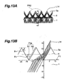
- the 100 ⁇ 100mm-scale dye-sensitized solar cell (the actual area S 0 of the photoreceptive surface F2; 96 ⁇ 96 mm and the thickness; 22 mm) was fabricated in the substantially same structure as the dye-sensitized solar cell 12 shown in Fig. 4, except for provision of the optical waveguide layer 5a in the shape shown in Fig. 12 (a) to (c), according to the substantially same procedure as in Example 1.
- Fig. 12 (a) is another sectional view of the optical waveguide layer 5a provided in this dye-sensitized solar cell
- Fig. 12 (b) a front view of the optical waveguide layer 5a shown in Fig. 12 (a), on the photo-electrode WE side
- Fig. 12 (c) an enlarged view of a partial region PR1 of the optical waveguide layer 5a shown in Fig. 12 (a).
- reflective facets F5a were formed at predetermined angles of inclination relative to the photoreceptive surface F1 of the transparent electrode 1 as described previously, in which the angle ⁇ 3 of inclination relative to the photoreceptive surface F1 of the transparent electrode 1 was 59° ⁇ 0.5° and in which the angle ⁇ 4 of inclination relative to the photoreceptive surface F1 of the transparent electrode 1 and the reflective face R1 formed in the lower local area was 63° ⁇ 0.5°.
- This optical waveguide layer 5a was designed so that there was no shielding loss of light quantity due to the comb-shaped electrodes 22 in the case of the configuration wherein the thickness of the glass (transparent electrode 1) forming the dye-sensitized solar cell was 1.1 mm, the refractive index thereof was 1.52, the width of the comb-shaped electrodes 22 was 0.5 mm, and the distance between the comb-shaped electrodes 22 was 12 mm.
- Fig. 13 shows the result of ray tracing where normal incident light was made incident to the optical waveguide layer 5a, wherein Fig. 13 (a) is a sectional view of the optical waveguide layer 5a. Fig. 13 (b) is an enlarged view of a partial region PR2 of the coating layer shown in (a).
- the effective energy conversion efficiency of this dye-sensitized solar cell was determined in much the same manner as in the cell characteristic tests described previously, and the result was 6.2%.
- the conventional dye-sensitized solar cell was fabricated in the substantially same structure as the dye-sensitized solar cell of Example 17, except that the optical waveguide layer 5a shown in Fig. 12 was not provided. Then the energy conversion efficiency of the solar cell was determined, and the result was 5.1%.
- the dye-sensitized solar cells and dye-sensitized solar cell modules according to the present invention are able surely to secure the sufficient utilization factors of incident light even with use of the thin semiconductor electrode and readily to reduce the deterioration of utilization factor of incident light due to decrease of the photoreceptive area satisfactorily even if they are scaled up or modularized. Accordingly, the present invention is able to provide the dye-sensitized solar cells and dye-sensitized solar cell modules having the excellent energy conversion efficiencies comparable to the amorphous silicon solar cells andbeing capable of generating electric power on a stable basis.
- FIG. 1 7 0 7.0 6722.4 2299.2 6.1 EXAMPLE 2 FIG. 1 4 5 7.0 3360 2376 5.6 EXAYPLE 3 FIG.
- FIG. 10 3 4 5 10.0 71.1 - 7.8 EXAMPLE 13
- FIG. 3 3 0 10.0 71.1 - 6.8 EXAMPLE 14
- FIG. 10 7 0 7.0 668160.0 228524.2
- FIG. 10 7 0 7.0 668160.0 228524.2
- FIG. 10 5 7.0 332560.0 228084.4
- FIG. 10 3 0 7.0 253440.0 219485.5 3.4
- COMPARATIVE EXAMPLE 1 FIG. 11 0 7 0 2304 2304 4.8 COMPARATIVE EXAMPLE 2
- FIG. 1 2 0 7.0 2400.7 2256 4.7 COMPARATIVE EXAMPLE 3
- FIG. 11 0 7 0 2304 2304 4.8
- FIG. 1 2 0 7.0 2400.7 2256 4.7
- COMPARATIVE EXAMPLE 3 FIG. 3 2 0 7.0 2304 - 4.9 COMP
- FIG. 3 0 20.0 73.47 - 6.8 COMPARATIVE EXAMPLE 5
- FIG. 3 2 0 20.0 73.47 - 6.7 COMPARATIVE EXAMPLE 6
- FIG. 3 8 5 20.0 73.47 - 2.1 COMPARATIVE EXAMPLE 7
- FIG. 3 0 10.0 71.1 - 6.5
- FIG. 3 2 0 10.0 71.1 - 6.4
- FIG. 3 8 5 10.0 71.1 - 2.0
- FIG. 10 0 7.0 230400.0 230400.0 3.4 COMPARATIVE EXAMPLE 11
- FIG. 10 2 0 7.0 230400.0 230400.0 3.2 COMPARATIVE EXAMPLE 12
- FIG. 10 8 5 7.0 230400.0 230400.0 0.1
Landscapes
- Engineering & Computer Science (AREA)
- Power Engineering (AREA)
- Microelectronics & Electronic Packaging (AREA)
- Chemical & Material Sciences (AREA)
- Chemical Kinetics & Catalysis (AREA)
- Electrochemistry (AREA)
- Hybrid Cells (AREA)
- Photovoltaic Devices (AREA)
Abstract
Description
| SEMICONDUCTOR ELECTRODE | ||||||
| CELL STRUCTURE | ANGLE OF INCIDENCE /° | THICKNESS OF ELECTRODE /µm | ACTUAL AREA OF PHOTORECEPTIVE SURFACE S0 /mm2 | PROJECTED AREA OF PHOTORECEPTIVE SURFACE S0 cos /mm2 | EFFECTIVE ENERGY CONVERSION EFFICIENCY η /% | |
| EXAMPLE 1 | FIG. 1 | 7 0 | 7.0 | 6722.4 | 2299.2 | 6.1 |
| EXAMPLE 2 | FIG. 1 | 4 5 | 7.0 | 3360 | 2376 | 5.6 |
| EXAYPLE 3 | FIG. 1 | 3 0 | 7.0 | 2443.3 | 2116 | 4.9 |
| EXAMPLE 4 | FIG.3 | 7 0 | 7.0 | 2304 | - | 6.2 |
| EXAMPLE 5 | FIG. 3 | 4 5 | 7.0 | 2304 | - | 5.8 |
| EXAMPLE 6 | FIG. 3 | 3 0 | 7.0 | 2304 | - | 5.1 |
| EXAMPLE 7 | FIC. 3 | 7 0 | 7.0 | 2304 | - | 6.3 |
| EXAMPLE 8 | FIG. 3 | 7 0 | 20.0 | 73.47 | - | 8.8 |
| EXAMPLE 9 | FIG. 3 | 4 5 | 20.0 | 73.47 | - | 8.2 |
| EXAMPLE 10 | FIG. 3 | 3 0 | 20.0 | 73.47 | - | 7.1 |
| EXAMPLE 11 | FIG. 3 | 7 0 | 10.0 | 71.1 | - | 8.5 |
| EXAMPLE 12. | FIG. 3 | 4 5 | 10.0 | 71.1 | - | 7.8 |
| EXAMPLE 13 | FIG. 3 | 3 0 | 10.0 | 71.1 | - | 6.8 |
| EXAMPLE 14 | FIG. 10 | 7 0 | 7.0 | 668160.0 | 228524.2 | 4.4 |
| EXAMPLE 15 | FIG. 10 | 4 5 | 7.0 | 332560.0 | 228084.4 | 4.1 |
| EXAMPLE 16 | FIG. 10 | 3 0 | 7.0 | 253440.0 | 219485.5 | 3.4 |
| COMPARATIVE EXAMPLE 1 | FIG. 11 | 0 | 7 0 | 2304 | 2304 | 4.8 |
| COMPARATIVE EXAMPLE 2 | FIG. 1 | 2 0 | 7.0 | 2400.7 | 2256 | 4.7 |
| COMPARATIVE EXAMPLE 3 | FIG. 3 | 2 0 | 7.0 | 2304 | - | 4.9 |
| COMPARATIVE EXAMPLE 4 | FIG. 3 | 0 | 20.0 | 73.47 | - | 6.8 |
| COMPARATIVE EXAMPLE 5 | FIG. 3 | 2 0 | 20.0 | 73.47 | - | 6.7 |
| COMPARATIVE EXAMPLE 6 | FIG. 3 | 8 5 | 20.0 | 73.47 | - | 2.1 |
| COMPARATIVE EXAMPLE 7 | FIG. 3 | 0 | 10.0 | 71.1 | - | 6.5 |
| COMPARATIVE EXAMPLE 8 | FIG. 3 | 2 0 | 10.0 | 71.1 | - | 6.4 |
| COMPARATIVE EXAMPLE 9 | FIG. 3 | 8 5 | 10.0 | 71.1 | - | 2.0 |
| COMPARATIVE EXAMPLE 10 | FIG. 10 | 0 | 7.0 | 230400.0 | 230400.0 | 3.4 |
| COMPARATIVE EXAMPLE 11 | FIG. 10 | 2 0 | 7.0 | 230400.0 | 230400.0 | 3.2 |
| COMPARATIVE EXAMPLE 12 | FIG. 10 | 8 5 | 7.0 | 230400.0 | 230400.0 | 0.1 |
Claims (10)
- A dye-sensitized solar cell which comprises a photo-electrode having a semiconductor electrode and a transparent electrode placed on a photoreceptive surface of the semiconductor electrode, and a counter electrode and in which said semiconductor electrode is opposed through an electrolyte to said counter electrode,
wherein said photoreceptive surface of said semiconductor electrode is formed so that an angle of incidence of light incident to said photoreceptive surface of said semiconductor electrode from a direction of a normal to a photoreceptive surface of said transparent electrode falls within a range of 30 to 80°. - A dye-sensitized solar cell which comprises a photo-electrode having a semiconductor electrode and a transparent electrode placed on a photoreceptive surface of the semiconductor electrode, and a counter electrode and in which said semiconductor electrode is opposed through an electrolyte to said counter electrode,
wherein said transparent electrode is provided with lightguide means for changing a traveling direction of light incident from the outside to a photoreceptive surface of said transparent electrode so that an angle of incidence of the light traveling in said transparent electrode to enter said photoreceptive surface of said semiconductor electrode falls within a range of 30 to 80°. - The dye-sensitized solar cell according to Claim 2, wherein said lightguide means is an optical waveguide layer formed on said photoreceptive surface of said transparent electrode and comprised of a plurality of glass fibers,
wherein each said glass fiber is placed with a predetermined inclination relative to a direction of a normal to said photoreceptive surface of said semiconductor electrode so that the angle of incidence of the light incident to said photoreceptive surface of said semiconductor electrode falls within the range of 30 to 80°. - The dye-sensitized solar cell according to Claim 2, wherein said lightguide means is an optical waveguide layer formed on said photoreceptive surface of said transparent electrode,
wherein a plurality of projections with reflective facets for changing the traveling direction of the light traveling in the optical waveguide layer are formed in a lower region of said optical waveguide layer in contact with said photoreceptive surface of said transparent electrode,
wherein each said reflective facet is formed with a predetermined inclination relative to said photoreceptive surface of said transparent electrode so that the angle of incidence of the light incident to said photoreceptive surface of said semiconductor electrode falls within the range of 30 to 80°. - The dye-sensitized solar cell according to Claim 4, wherein a plurality of collecting electrodes are further provided on said photoreceptive surface of said semiconductor electrode,
wherein each said reflective facet is formed with the predetermined inclination relative to said photoreceptive surface of said transparent electrode so that the angle of incidence of the light incident to said photoreceptive surface of said semiconductor electrode falls within the range of 30 to 80° and so that said light selectively impinges on areas without said collecting electrodes on said photoreceptive surface of said semiconductor electrode. - The dye-sensitized solar cell according to Claim 2, wherein said lightguide means is a plurality of reflective portions with reflective facets formed in said transparent electrode and adapted to change the traveling direction of the light traveling in said transparent electrode,
wherein each said reflective facet is formed with a predetermined inclination relative to a direction of a normal to said photoreceptive surface of said semiconductor electrode so that the angle of incidence of the light incident to said photoreceptive surface of said semiconductor electrode falls within the range of 30 to 80°. - The dye-sensitized solar cell according to Claim 2, wherein said lightguide means is a plurality of projections with reflective facets formed on saidphotoreceptive surface of said transparent electrode and adapted to change the traveling direction of the light incident from a direction of a normal to the photoreceptive surface of said semiconductor electrode,
wherein each said reflective facet is formed with a predetermined inclination relative to the direction of the normal to said photoreceptive surface of said semiconductor electrode so that the angle of incidence of the light incident to said photoreceptive surface of said semiconductor electrode falls within the range of 30 to 80°. - The dye-sensitized solar cell according to Claim 2, wherein said lightguide means is a plurality of diffraction grating stripes formed on the photoreceptive surface of said transparent electrode and made of a transparent material having a refractive index higher than that of said transparent electrode,
wherein said diffraction grating stripes diffract the light incident from a direction of a normal to said photoreceptive surface of said semiconductor electrode, into predetermined angles so that angles of incidence of the light incident to said photoreceptive surface of said semiconductor electrode fall within the range of 30 to 80°. - A dye-sensitized solar cell which comprises a photo-electrode having a semiconductor electrode and a transparent electrode placed on a photoreceptive surface of the semiconductor electrode, and a counter electrode and in which said semiconductor electrode is opposed through an electrolyte to said counter electrode,
wherein a plurality of collecting electrodes are provided on said photoreceptive surface of said semiconductor electrode,
wherein said photoreceptive surface of said semiconductor electrode is formed so that an angle of incidence of light traveling in said transparent electrode to enter said photoreceptive surface of said semiconductor electrode falls within a range of 30 to 80°, and
wherein a photoreceptive surface of said transparent electrode is formed so that said light selectively impinges on areas without said collecting electrodes on said photoreceptive surface of said semiconductor electrode. - A dye-sensitized solar cell module comprising a plurality of dye-sensitized solar cells placed on a base, each said dye-sensitized solar cell comprising a photo-electrode having a semiconductor electrode and a transparent electrode placed on a photoreceptive surface of the semiconductor electrode, and a counter electrode and in each said dye-sensitized solar cell said semiconductor electrode being opposed through an electrolyte to said counter electrode,
wherein each said dye-sensitized solar cell is placed so that an angle of incidence of light incident to each said dye-sensitized solar cell from a direction of a normal to an installation surface of said base falls within a range of 30 to 80°.
Applications Claiming Priority (2)
| Application Number | Priority Date | Filing Date | Title |
|---|---|---|---|
| JP2001055110 | 2001-02-28 | ||
| JP2001055110A JP4213355B2 (en) | 2001-02-28 | 2001-02-28 | Dye-sensitized solar cell and dye-sensitized solar cell module |
Publications (2)
| Publication Number | Publication Date |
|---|---|
| EP1237166A2 true EP1237166A2 (en) | 2002-09-04 |
| EP1237166A3 EP1237166A3 (en) | 2005-03-16 |
Family
ID=18915343
Family Applications (1)
| Application Number | Title | Priority Date | Filing Date |
|---|---|---|---|
| EP02004524A Withdrawn EP1237166A3 (en) | 2001-02-28 | 2002-02-27 | Dye-sensitized solar cells and dye-sensitized solar cell modules |
Country Status (2)
| Country | Link |
|---|---|
| EP (1) | EP1237166A3 (en) |
| JP (1) | JP4213355B2 (en) |
Cited By (16)
| Publication number | Priority date | Publication date | Assignee | Title |
|---|---|---|---|---|
| EP1341197A3 (en) * | 2002-02-28 | 2004-12-15 | Fuji Photo Film Co., Ltd. | Film of fine semiconductor particles for a photoelectrochemical cell |
| EP1562205A1 (en) * | 2004-02-03 | 2005-08-10 | Samsung SDI Co., Ltd. | DYE-Sensitized solar cell and method of manufacturing the same |
| EP1643516A1 (en) * | 2004-09-30 | 2006-04-05 | Enplas Corporation | Photoelectrode for dye sensitizing solar cell or organic solar cell |
| US7145071B2 (en) * | 2002-12-11 | 2006-12-05 | General Electric Company | Dye sensitized solar cell having finger electrodes |
| WO2008092679A1 (en) * | 2007-02-01 | 2008-08-07 | Leonhard Kurz Stiftung & Co. Kg | Solar cell |
| WO2009062837A1 (en) * | 2007-11-16 | 2009-05-22 | Nanogate Advanced Materials Gmbh | Solar cell having optical amplifier structures |
| EP2051266A3 (en) * | 2007-10-18 | 2011-11-02 | Electronics and Telecommunications Research Institute | Dye-sensitized solar cell and method of fabricating the same |
| EP2452350A1 (en) * | 2009-07-09 | 2012-05-16 | NLAB Solar AB | Dye sensitized solar cell with improved optical characteristics |
| CN102484152A (en) * | 2009-04-09 | 2012-05-30 | 加利福尼亚大学董事会 | Three-dimensional dye-sensitized solar cells with nanoscale structures |
| EP2330636A3 (en) * | 2009-12-01 | 2013-04-17 | Samsung SDI Co., Ltd. | Dye-sensitized solar concentrator module |
| EP2387800A4 (en) * | 2009-01-16 | 2013-12-11 | Genie Lens Technologies Llc | PHOTOVOLTAIC (PV) ENHANCEMENT FILMS FOR IMPROVING OPTICAL PATH LENGTHS AND METHODS OF MANUFACTURING PV ENHANCEMENT FILMS |
| WO2014027908A1 (en) * | 2012-08-13 | 2014-02-20 | ML SYSTEM Spółka z ograniczoną odpowiedzialnością | A dye sensitized solar cell module and a method of its manufacturing |
| US8674209B2 (en) | 2007-12-21 | 2014-03-18 | Jusung Engineering Co., Ltd. | Thin film type solar cell and method for manufacturing the same |
| RU2529826C2 (en) * | 2013-01-15 | 2014-09-27 | Открытое акционерное ощество "Научно-производственное предприятие Квант" | Solar cell having diffraction grating on front surface |
| EP1905099A4 (en) * | 2005-07-15 | 2017-07-19 | Merck Patent GmbH | Diffraction foils |
| EP2395597B1 (en) * | 2009-02-03 | 2019-12-18 | Showa Co., Ltd. | Dye-sensitized solar cell |
Families Citing this family (34)
| Publication number | Priority date | Publication date | Assignee | Title |
|---|---|---|---|---|
| JP4606777B2 (en) * | 2004-05-31 | 2011-01-05 | 株式会社フジクラ | Wet solar cell |
| JP2006147261A (en) * | 2004-11-17 | 2006-06-08 | Enplas Corp | Counter electrode of dye-sensitized solar cell and dye-sensitized solar cell |
| JP4754862B2 (en) * | 2005-04-15 | 2011-08-24 | シャープ株式会社 | Dye-sensitized solar cell and method for producing the same |
| JP5005206B2 (en) * | 2005-10-20 | 2012-08-22 | 株式会社フジクラ | Working electrode of dye-sensitized solar cell, dye-sensitized solar cell including the same, and method for producing working electrode of dye-sensitized solar cell |
| KR100728194B1 (en) | 2005-11-11 | 2007-06-13 | 삼성에스디아이 주식회사 | Dye-sensitized solar cell and method for producing same |
| JP5148835B2 (en) * | 2006-03-29 | 2013-02-20 | 株式会社エンプラス | Dye-sensitized solar cell and its photoelectrode substrate |
| KR100935322B1 (en) * | 2008-01-02 | 2010-01-06 | 삼성전기주식회사 | High efficiency solar cell and its manufacturing method |
| JP5208974B2 (en) * | 2008-02-06 | 2013-06-12 | 株式会社フジクラ | Dye-sensitized solar cell |
| CN102265453B (en) | 2008-10-29 | 2014-10-01 | 富士胶片株式会社 | Dye, photoelectric conversion element using the same, photoelectrochemical cell, and method for producing the dye |
| JP5524557B2 (en) | 2009-09-28 | 2014-06-18 | 富士フイルム株式会社 | Method for producing photoelectric conversion element, photoelectric conversion element, and photoelectrochemical cell |
| JP5620081B2 (en) | 2009-09-28 | 2014-11-05 | 富士フイルム株式会社 | Method for manufacturing photoelectric conversion element |
| JP2011076869A (en) * | 2009-09-30 | 2011-04-14 | Tdk Corp | Dye-sensitized solar cell, method of manufacturing the same, and method of manufacturing working electrode for dye-sensitized solar cell |
| JP2011204464A (en) * | 2010-03-25 | 2011-10-13 | Casio Computer Co Ltd | Dye-sensitized solar cell |
| JP5561641B2 (en) * | 2010-05-10 | 2014-07-30 | 国立大学法人 新潟大学 | Dye-sensitized solar cell |
| JP4980479B2 (en) | 2010-06-02 | 2012-07-18 | 富士フイルム株式会社 | Metal complex dye, photoelectric conversion element, and dye-sensitized solar cell |
| US10424678B2 (en) | 2011-01-10 | 2019-09-24 | Toyota Motor Engineering & Manufacturing North America, Inc. | Solar cell with double groove diffraction grating |
| JP5756772B2 (en) | 2011-03-30 | 2015-07-29 | 富士フイルム株式会社 | Photoelectric conversion element and photoelectrochemical cell |
| JP5245001B2 (en) | 2011-09-29 | 2013-07-24 | 富士フイルム株式会社 | Photoelectric conversion element, photoelectrochemical cell, and metal complex dye used therefor |
| JP5881578B2 (en) | 2011-12-15 | 2016-03-09 | 富士フイルム株式会社 | Metal complex dye, photoelectric conversion element, dye-sensitized solar cell, and dye solution |
| JP2013161751A (en) | 2012-02-08 | 2013-08-19 | Fujifilm Corp | Photoelectric conversion element, method of manufacturing the same, and dye-sensitized solar cell using the same |
| JP5925541B2 (en) | 2012-03-16 | 2016-05-25 | 富士フイルム株式会社 | Metal complex dye for photoelectric conversion element, photoelectric conversion element, dye-sensitized solar cell, dye-adsorbing composition liquid for dye-sensitized solar cell, semiconductor electrode for dye-sensitized solar cell, and method for producing dye-sensitized solar cell |
| JP5201287B1 (en) * | 2012-08-31 | 2013-06-05 | 大日本印刷株式会社 | Dye-sensitized solar cell and method for producing dye-sensitized solar cell |
| JP2014082187A (en) | 2012-09-28 | 2014-05-08 | Fujifilm Corp | Photoelectric conversion element and dye-sensitized solar cell |
| JP5913222B2 (en) | 2012-09-28 | 2016-04-27 | 富士フイルム株式会社 | Photoelectric conversion element and dye-sensitized solar cell |
| JP6063359B2 (en) | 2012-09-28 | 2017-01-18 | 富士フイルム株式会社 | Photoelectric conversion element, dye-sensitized solar cell, metal complex dye and dye solution formed by dissolving metal complex dye |
| JP5913223B2 (en) | 2012-09-28 | 2016-04-27 | 富士フイルム株式会社 | Metal complex dye, photoelectric conversion element, dye-sensitized solar cell, dye solution and dye-adsorbing electrode |
| JP5992389B2 (en) | 2012-11-16 | 2016-09-14 | 富士フイルム株式会社 | Photoelectric conversion element, dye-sensitized solar cell, metal complex dye, dye solution, dye-adsorbing electrode, and method for producing dye-sensitized solar battery |
| JP5944372B2 (en) | 2012-12-17 | 2016-07-05 | 富士フイルム株式会社 | Photoelectric conversion element, dye-sensitized solar cell, metal complex dye, dye solution, dye-adsorbing electrode, and method for producing dye-sensitized solar battery |
| JP5972811B2 (en) | 2013-02-22 | 2016-08-17 | 富士フイルム株式会社 | Photoelectric conversion element, method for producing photoelectric conversion element, and dye-sensitized solar cell |
| JP6047513B2 (en) | 2013-03-25 | 2016-12-21 | 富士フイルム株式会社 | Metal complex dye, photoelectric conversion element, dye-sensitized solar cell, and dye solution containing metal complex dye |
| WO2018061983A1 (en) | 2016-09-29 | 2018-04-05 | 富士フイルム株式会社 | Photoelectric conversion element, dye-sensitized solar cell, metal complex dye, dye solution, and oxide semiconductor electrode |
| WO2018092740A1 (en) * | 2016-11-15 | 2018-05-24 | 株式会社フジクラ | Photoelectric conversion element |
| EP3584814A4 (en) | 2017-02-17 | 2020-12-16 | Fujifilm Corporation | Photoelectric conversion element, dye-sensitized solar cell, metal complex dye, dye composition, and oxide semiconductor electrode |
| EP3627577A4 (en) | 2017-05-19 | 2020-06-17 | FUJIFILM Corporation | Photoelectric conversion element, solar cell, method for producing photoelectric conversion element, and composition for forming photosensitive layer |
Family Cites Families (3)
| Publication number | Priority date | Publication date | Assignee | Title |
|---|---|---|---|---|
| US5110370A (en) * | 1990-09-20 | 1992-05-05 | United Solar Systems Corporation | Photovoltaic device with decreased gridline shading and method for its manufacture |
| DE9308513U1 (en) * | 1993-05-25 | 1994-01-20 | Hoffmann, Thomas, 12559 Berlin | Arrangement for a series connection of photoelectrochemical (PEC) solar cells |
| US5500054A (en) * | 1995-01-10 | 1996-03-19 | Quantum Group, Inc. | Superemissive light pipes and photovoltaic systems including same |
-
2001
- 2001-02-28 JP JP2001055110A patent/JP4213355B2/en not_active Expired - Fee Related
-
2002
- 2002-02-27 EP EP02004524A patent/EP1237166A3/en not_active Withdrawn
Cited By (18)
| Publication number | Priority date | Publication date | Assignee | Title |
|---|---|---|---|---|
| EP1341197A3 (en) * | 2002-02-28 | 2004-12-15 | Fuji Photo Film Co., Ltd. | Film of fine semiconductor particles for a photoelectrochemical cell |
| US7145071B2 (en) * | 2002-12-11 | 2006-12-05 | General Electric Company | Dye sensitized solar cell having finger electrodes |
| EP1562205A1 (en) * | 2004-02-03 | 2005-08-10 | Samsung SDI Co., Ltd. | DYE-Sensitized solar cell and method of manufacturing the same |
| EP1643516A1 (en) * | 2004-09-30 | 2006-04-05 | Enplas Corporation | Photoelectrode for dye sensitizing solar cell or organic solar cell |
| EP1905099A4 (en) * | 2005-07-15 | 2017-07-19 | Merck Patent GmbH | Diffraction foils |
| WO2008092679A1 (en) * | 2007-02-01 | 2008-08-07 | Leonhard Kurz Stiftung & Co. Kg | Solar cell |
| EP2051266A3 (en) * | 2007-10-18 | 2011-11-02 | Electronics and Telecommunications Research Institute | Dye-sensitized solar cell and method of fabricating the same |
| WO2009062837A1 (en) * | 2007-11-16 | 2009-05-22 | Nanogate Advanced Materials Gmbh | Solar cell having optical amplifier structures |
| US8674209B2 (en) | 2007-12-21 | 2014-03-18 | Jusung Engineering Co., Ltd. | Thin film type solar cell and method for manufacturing the same |
| EP2387800A4 (en) * | 2009-01-16 | 2013-12-11 | Genie Lens Technologies Llc | PHOTOVOLTAIC (PV) ENHANCEMENT FILMS FOR IMPROVING OPTICAL PATH LENGTHS AND METHODS OF MANUFACTURING PV ENHANCEMENT FILMS |
| EP2395597B1 (en) * | 2009-02-03 | 2019-12-18 | Showa Co., Ltd. | Dye-sensitized solar cell |
| CN102484152A (en) * | 2009-04-09 | 2012-05-30 | 加利福尼亚大学董事会 | Three-dimensional dye-sensitized solar cells with nanoscale structures |
| CN102484152B (en) * | 2009-04-09 | 2015-11-25 | 加利福尼亚大学董事会 | Three-dimensional dye-sensitized solar cells with nanoscale structures |
| US9368289B2 (en) | 2009-04-09 | 2016-06-14 | The Regents Of The University Of California | Three dimensional dye-sensitized solar cells with nanoscale architectures |
| EP2452350A1 (en) * | 2009-07-09 | 2012-05-16 | NLAB Solar AB | Dye sensitized solar cell with improved optical characteristics |
| EP2330636A3 (en) * | 2009-12-01 | 2013-04-17 | Samsung SDI Co., Ltd. | Dye-sensitized solar concentrator module |
| WO2014027908A1 (en) * | 2012-08-13 | 2014-02-20 | ML SYSTEM Spółka z ograniczoną odpowiedzialnością | A dye sensitized solar cell module and a method of its manufacturing |
| RU2529826C2 (en) * | 2013-01-15 | 2014-09-27 | Открытое акционерное ощество "Научно-производственное предприятие Квант" | Solar cell having diffraction grating on front surface |
Also Published As
| Publication number | Publication date |
|---|---|
| JP4213355B2 (en) | 2009-01-21 |
| JP2002260746A (en) | 2002-09-13 |
| EP1237166A3 (en) | 2005-03-16 |
Similar Documents
| Publication | Publication Date | Title |
|---|---|---|
| EP1237166A2 (en) | Dye-sensitized solar cells and dye-sensitized solar cell modules | |
| Ying et al. | Towards the 10‐year milestone of monolithic perovskite/silicon tandem solar cells | |
| JP5089605B2 (en) | Notch filter for triple junction solar cells | |
| US9070811B2 (en) | Multi-crystalline II-VI based multijunction solar cells and modules | |
| EP3679607B1 (en) | Organic-inorganic perovskite materials and methods of making the same | |
| US9653630B2 (en) | Quantum dot solar cell performance with a metal salt treatment | |
| JPS59104185A (en) | Photovoltaic semiconductor device spaced with reflector | |
| KR101724692B1 (en) | Manufacturing method of titanium dioxide nanorod using hydrothermal method and photoelectrode comprising titanium dioxide nanorod prepared therefrom | |
| CN114267797B (en) | A preparation method and application of flexible and special-shaped perovskite solar cell module | |
| KR20150052759A (en) | Improving quantum dot solar cell performance with a metal salt treatment | |
| US12419153B2 (en) | Solar cell and method for manufacturing the same | |
| EP4300602A1 (en) | Perovskite solar cell and preparation method therefor | |
| CN118265408A (en) | A method for preparing wide bandgap perovskite film | |
| Hossain et al. | Revealing the full potential of CsPbIBr 2 perovskite solar cells: advancements towards enhanced performance | |
| US12581788B2 (en) | Solar cell and solar cell module including the same | |
| EP4300603A1 (en) | Perovskite solar cell and preparation method therefor | |
| EP4498783A1 (en) | Concentration-type perovskite solar assembly | |
| Laalioui | Perovskite-Based Solar Cells: From Fundamentals to Tandem Devices | |
| EP4593088A1 (en) | Tandem solar cell and method for manufacturing same | |
| JP2005310821A (en) | Photoelectric conversion element | |
| US20220302330A1 (en) | Solar cell and method for manufacturing the same | |
| CN212695178U (en) | Perovskite photovoltaic cell | |
| JP4939498B2 (en) | Dye-sensitized solar cell | |
| TWI511319B (en) | Method for manufacturing concentrating photovoltaic system | |
| Zhang et al. | Triple-junction all-perovskite solar cells: a review |
Legal Events
| Date | Code | Title | Description |
|---|---|---|---|
| PUAI | Public reference made under article 153(3) epc to a published international application that has entered the european phase |
Free format text: ORIGINAL CODE: 0009012 |
|
| 17P | Request for examination filed |
Effective date: 20020227 |
|
| AK | Designated contracting states |
Kind code of ref document: A2 Designated state(s): AT BE CH CY DE DK ES FI FR GB GR IE IT LI LU MC NL PT SE TR |
|
| AX | Request for extension of the european patent |
Free format text: AL;LT;LV;MK;RO;SI |
|
| PUAL | Search report despatched |
Free format text: ORIGINAL CODE: 0009013 |
|
| AK | Designated contracting states |
Kind code of ref document: A3 Designated state(s): AT BE CH CY DE DK ES FI FR GB GR IE IT LI LU MC NL PT SE TR |
|
| AX | Request for extension of the european patent |
Extension state: AL LT LV MK RO SI |
|
| RIC1 | Information provided on ipc code assigned before grant |
Ipc: 7H 01L 31/052 B Ipc: 7H 01L 31/0236 B Ipc: 7H 01G 9/20 A |
|
| AKX | Designation fees paid |
Designated state(s): CH DE GB LI |
|
| RIN1 | Information on inventor provided before grant (corrected) |
Inventor name: TOYODA, TATSUO Inventor name: NISHIMURA, KAZUHIKO Inventor name: DOI, SHOICHI Inventor name: TSUKIGASE, AZUSA,K.K. TOYOTA CHUO KENKYUSHO Inventor name: INABA, TADASHI,K.K. TOYOTA CHUO KENKYUSHO Inventor name: TAKEDA, YASUHIKO,K.K. TOYOTA CHUO KENKYUSHO Inventor name: AZUMA, HIROZUMI,K.K. TOYOTA CHUO KENKYUSHO Inventor name: HIGUCHI, KAZUO,K.K. TOYOTA CHUO KENKYUSHO Inventor name: MOTOHIRO, TOMOYOSHI,K.K. TOYOTA CHUO KENKYUSHO |
|
| 17Q | First examination report despatched |
Effective date: 20080519 |
|
| STAA | Information on the status of an ep patent application or granted ep patent |
Free format text: STATUS: THE APPLICATION IS DEEMED TO BE WITHDRAWN |
|
| 18D | Application deemed to be withdrawn |
Effective date: 20080930 |