EP1235257A1 - Semiconductor-manufacturing apparatus - Google Patents
Semiconductor-manufacturing apparatus Download PDFInfo
- Publication number
- EP1235257A1 EP1235257A1 EP00969956A EP00969956A EP1235257A1 EP 1235257 A1 EP1235257 A1 EP 1235257A1 EP 00969956 A EP00969956 A EP 00969956A EP 00969956 A EP00969956 A EP 00969956A EP 1235257 A1 EP1235257 A1 EP 1235257A1
- Authority
- EP
- European Patent Office
- Prior art keywords
- wafer
- susceptor
- heating
- substrate
- manufacturing apparatus
- Prior art date
- Legal status (The legal status is an assumption and is not a legal conclusion. Google has not performed a legal analysis and makes no representation as to the accuracy of the status listed.)
- Granted
Links
Images



Classifications
-
- H—ELECTRICITY
- H10—SEMICONDUCTOR DEVICES; ELECTRIC SOLID-STATE DEVICES NOT OTHERWISE PROVIDED FOR
- H10P—GENERIC PROCESSES OR APPARATUS FOR THE MANUFACTURE OR TREATMENT OF DEVICES COVERED BY CLASS H10
- H10P72/00—Handling or holding of wafers, substrates or devices during manufacture or treatment thereof
- H10P72/70—Handling or holding of wafers, substrates or devices during manufacture or treatment thereof for supporting or gripping
- H10P72/76—Handling or holding of wafers, substrates or devices during manufacture or treatment thereof for supporting or gripping using mechanical means, e.g. clamps or pinches
- H10P72/7604—Handling or holding of wafers, substrates or devices during manufacture or treatment thereof for supporting or gripping using mechanical means, e.g. clamps or pinches the wafers being placed on a susceptor, stage or support
-
- H—ELECTRICITY
- H10—SEMICONDUCTOR DEVICES; ELECTRIC SOLID-STATE DEVICES NOT OTHERWISE PROVIDED FOR
- H10P—GENERIC PROCESSES OR APPARATUS FOR THE MANUFACTURE OR TREATMENT OF DEVICES COVERED BY CLASS H10
- H10P72/00—Handling or holding of wafers, substrates or devices during manufacture or treatment thereof
- H10P72/70—Handling or holding of wafers, substrates or devices during manufacture or treatment thereof for supporting or gripping
- H10P72/76—Handling or holding of wafers, substrates or devices during manufacture or treatment thereof for supporting or gripping using mechanical means, e.g. clamps or pinches
- H10P72/7604—Handling or holding of wafers, substrates or devices during manufacture or treatment thereof for supporting or gripping using mechanical means, e.g. clamps or pinches the wafers being placed on a susceptor, stage or support
- H10P72/7611—Handling or holding of wafers, substrates or devices during manufacture or treatment thereof for supporting or gripping using mechanical means, e.g. clamps or pinches the wafers being placed on a susceptor, stage or support characterised by edge profile or support profile
-
- C—CHEMISTRY; METALLURGY
- C23—COATING METALLIC MATERIAL; COATING MATERIAL WITH METALLIC MATERIAL; CHEMICAL SURFACE TREATMENT; DIFFUSION TREATMENT OF METALLIC MATERIAL; COATING BY VACUUM EVAPORATION, BY SPUTTERING, BY ION IMPLANTATION OR BY CHEMICAL VAPOUR DEPOSITION, IN GENERAL; INHIBITING CORROSION OF METALLIC MATERIAL OR INCRUSTATION IN GENERAL
- C23C—COATING METALLIC MATERIAL; COATING MATERIAL WITH METALLIC MATERIAL; SURFACE TREATMENT OF METALLIC MATERIAL BY DIFFUSION INTO THE SURFACE, BY CHEMICAL CONVERSION OR SUBSTITUTION; COATING BY VACUUM EVAPORATION, BY SPUTTERING, BY ION IMPLANTATION OR BY CHEMICAL VAPOUR DEPOSITION, IN GENERAL
- C23C16/00—Chemical coating by decomposition of gaseous compounds, without leaving reaction products of surface material in the coating, i.e. chemical vapour deposition [CVD] processes
- C23C16/44—Chemical coating by decomposition of gaseous compounds, without leaving reaction products of surface material in the coating, i.e. chemical vapour deposition [CVD] processes characterised by the method of coating
- C23C16/458—Chemical coating by decomposition of gaseous compounds, without leaving reaction products of surface material in the coating, i.e. chemical vapour deposition [CVD] processes characterised by the method of coating characterised by the method used for supporting substrates in the reaction chamber
- C23C16/4582—Rigid and flat substrates, e.g. plates or discs
- C23C16/4583—Rigid and flat substrates, e.g. plates or discs the substrate being supported substantially horizontally
-
- C—CHEMISTRY; METALLURGY
- C23—COATING METALLIC MATERIAL; COATING MATERIAL WITH METALLIC MATERIAL; CHEMICAL SURFACE TREATMENT; DIFFUSION TREATMENT OF METALLIC MATERIAL; COATING BY VACUUM EVAPORATION, BY SPUTTERING, BY ION IMPLANTATION OR BY CHEMICAL VAPOUR DEPOSITION, IN GENERAL; INHIBITING CORROSION OF METALLIC MATERIAL OR INCRUSTATION IN GENERAL
- C23C—COATING METALLIC MATERIAL; COATING MATERIAL WITH METALLIC MATERIAL; SURFACE TREATMENT OF METALLIC MATERIAL BY DIFFUSION INTO THE SURFACE, BY CHEMICAL CONVERSION OR SUBSTITUTION; COATING BY VACUUM EVAPORATION, BY SPUTTERING, BY ION IMPLANTATION OR BY CHEMICAL VAPOUR DEPOSITION, IN GENERAL
- C23C16/00—Chemical coating by decomposition of gaseous compounds, without leaving reaction products of surface material in the coating, i.e. chemical vapour deposition [CVD] processes
- C23C16/44—Chemical coating by decomposition of gaseous compounds, without leaving reaction products of surface material in the coating, i.e. chemical vapour deposition [CVD] processes characterised by the method of coating
- C23C16/46—Chemical coating by decomposition of gaseous compounds, without leaving reaction products of surface material in the coating, i.e. chemical vapour deposition [CVD] processes characterised by the method of coating characterised by the method used for heating the substrate
-
- H—ELECTRICITY
- H10—SEMICONDUCTOR DEVICES; ELECTRIC SOLID-STATE DEVICES NOT OTHERWISE PROVIDED FOR
- H10P—GENERIC PROCESSES OR APPARATUS FOR THE MANUFACTURE OR TREATMENT OF DEVICES COVERED BY CLASS H10
- H10P72/00—Handling or holding of wafers, substrates or devices during manufacture or treatment thereof
- H10P72/04—Apparatus for manufacture or treatment
- H10P72/0431—Apparatus for thermal treatment
- H10P72/0436—Apparatus for thermal treatment mainly by radiation
-
- H—ELECTRICITY
- H10—SEMICONDUCTOR DEVICES; ELECTRIC SOLID-STATE DEVICES NOT OTHERWISE PROVIDED FOR
- H10P—GENERIC PROCESSES OR APPARATUS FOR THE MANUFACTURE OR TREATMENT OF DEVICES COVERED BY CLASS H10
- H10P72/00—Handling or holding of wafers, substrates or devices during manufacture or treatment thereof
- H10P72/70—Handling or holding of wafers, substrates or devices during manufacture or treatment thereof for supporting or gripping
- H10P72/74—Handling or holding of wafers, substrates or devices during manufacture or treatment thereof for supporting or gripping using temporarily an auxiliary support
Definitions
- the present invention relates to a semiconductor manufacturing apparatus with a susceptor for holding and heating a semiconductor wafer (substrate).
- Semiconductor manufacturing apparatuses include one called a single wafer processing type semiconductor manufacturing apparatus for processing silicon wafers one by one.
- a wafer support unit for horizontally supporting only one wafer is usually arranged in a process chamber.
- the wafer support unit generally has a susceptor (substrate holding table) where a wafer is placed.
- the susceptor is heated by a heating means such as a lamp, and the wafer is heated through the susceptor.
- the wafer support unit also has a lift mechanism for vertically moving the wafer placed on the susceptor with respect to the susceptor.
- the lift mechanism has a plurality of lift pins extending through the susceptor. When the wafer is placed on the upper ends of the lift pins and the lift pins are vertically moved, the wafer can be vertically moved.
- the lift mechanism can transfer a wafer transferred on the blade of a transfer robot onto the susceptor, or can conversely transfer a wafer from the susceptor to the transfer robot.
- the planar temperature of the susceptor serving as the holding table and used for heating the wafer must be uniformed.
- a method of adjusting the temperature distribution a method of obtaining temperature uniformity by adjusting the heating condition for the susceptor is available, e.g., by adjusting the irradiating condition of the heating light from a lamp in the case of lamp heating.
- the heating adjusting method becomes complicated.
- a sufficiently high temperature uniformity cannot be obtained.
- a nonuniform planar temperature distribution occurs in the wafer due to various factors.
- the condition of heat conduction from the susceptor to the wafer sometimes differs between the center and periphery of the susceptor. It is difficult to obtain temperature uniformity by adjusting all the heating conditions for the wafer in accordance with the heating condition for the susceptor.
- the planar temperature becomes nonuniform in the wafer
- the film deposition condition becomes nonuniform within the wafer surface. Accordingly, nonuniformity occurs in the distribution of the thickness of the formed film.
- the present invention has been made in view of the above problems, and has as its object to provide a semiconductor manufacturing apparatus using a susceptor that improves the uniformity of the planar temperature distribution of a semiconductor wafer (substrate) as a processing target.
- the present inventors have conducted intensive studies. Consequently, the present inventors have found that when a three-dimensional structure is added to the planar shape of the upper surface of the susceptor in the wafer holding area, the planar temperature distribution of the wafer is adjusted, and the temperature distribution is uniformed, so that the uniformity of the thickness distribution of the formed film can be improved, thus reaching the present invention.
- a semiconductor manufacturing apparatus is a semiconductor manufacturing apparatus comprising a process chamber, a susceptor set in the process chamber to hold a target substrate in a substrate holding area on an upper surface thereof and heat the target substrate, and heating means for heating the target substrate through the susceptor, characterized in that the susceptor supports the target substrate with a substrate support member so as to form, in the substrate holding area, a gap with a first distance between a substrate heating surface as that surface portion of the upper surface of the susceptor which opposes the target substrate and a lower surface of the target substrate, and a heating adjusting portion for forming a gap with a second distance different from the first distance is formed at a predetermined portion on the substrate heating surface.
- the substrate in the susceptor for holding a substrate (target substrate) as a processing target such as a semiconductor wafer or glass substrate, the substrate is held by forming a gap between the target substrate and the substrate heating surface. This decreases influences on the temperature distribution of the substrate such as the local three-dimensional structure on the substrate heating surface and the nonuniformity of the temperature distribution.
- a recessed or projecting heating adjusting portion with a different gap distance is formed in the substrate heating surface, so that the distance of the gap between the target substrate and substrate heating surface is positively imparted with a distribution.
- the heating conditions for the target substrate at the respective portions of the substrate heating surface are set and adjusted, so that the planar temperature distribution of the substrate such as a wafer can be uniformed so as to obtain a uniform formed film thickness distribution.
- Fig. 1 schematically shows a film deposition apparatus such as an epitaxial growth apparatus as a semiconductor manufacturing apparatus according to the present invention.
- a film deposition apparatus 10 shown in Fig. 1 is a single wafer processing type apparatus for processing silicon wafers (not shown in Fig. 1) as target substrates one by one.
- An example of the target substrate includes a semiconductor wafer and glass substrate. A case wherein the target substrate is a silicon wafer will be described hereinafter.
- the film deposition apparatus 10 has a process chamber 12 made of silica glass, and a wafer support unit 14 is set in the process chamber 12.
- a process gas inlet port 16 is formed in the side portion of the process chamber 12, and an exhaust port 18 is formed in the process chamber 12 at a position opposing it.
- a plurality of, e.g., 20, halogen lamps 20 serving as a heating means are radially arranged in the lower region of the process chamber 12.
- a wafer is supported by the wafer support unit 14.
- the halogen lamps 20 are turned on to heat the wafer, and a process gas is introduced from the inlet port 16 while performing evacuation from the exhaust port 18. Then, the process gas flows in the form of a laminar flow along the surface of the wafer heated to a predetermined temperature, and silicon single crystals epitaxially grow on the wafer.
- the process gas to be supplied for example, one obtained by mixing a silicon source gas such as SiH 4 , Si 2 H 6 , or SiH 2 Cl 2 , a dopant gas such as PH 3 , AsH 3 , or B 2 H 6 , and a carrier gas such as H 2 or N 2 in a gas panel (not shown) is used.
- the pressure in the process chamber 12 is adjusted to 0.7 kPa (5 Torr) to 88 kPa (660 Torr) by means of the aperture ratio of the throttle valve in the exhaust pipe.
- the wafer support unit 14 applied to the film deposition apparatus 10 shown in Fig. 1 has a susceptor 22 as a holding table for holding the wafer.
- the susceptor 22 is a disk-like one made of a graphite material and covered with silicon carbide, and is horizontally supported by a support shaft 24, made of quartz glass and standing upright in the lower portion of the process chamber 12, at three points from its lower surface.
- the susceptor 22 is used for holding and heating the wafer.
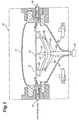
- Figs. 2A and 2B are side sectional and upper plan views, respectively, showing the arrangement of the susceptor 22.
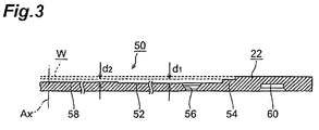
- Fig. 3 is a partly enlarged side sectional view showing the right portion of the susceptor 22 shown in Fig. 2A.
- Fig. 2A shows the wafer W in a supported state
- Fig. 3 shows, with a dashed line, a position where the wafer W is supported
- Fig. 2B shows the structure of the susceptor 22 that does not support the wafer W.
- a substantially circular wafer holding area (substrate holding area) 50 for accommodating and holding the wafer W is set on the upper surface of the susceptor 22 about a central axis Ax of the disk-like susceptor 22 as the center.
- a wafer heating surface (substrate heating surface) 52 formed of a circular recess about the central axis Ax as the center is formed in the wafer holding area 50.
- a susceptor support 60 for supporting the susceptor 22 with the support shaft 24 is formed in that lower surface of the susceptor 22 which is outside the wafer holding area 50.
- An annular projecting step is formed on the periphery of the wafer heating surface 52 along the outer circumference of the wafer heating surface 52.
- This annular step is a wafer support (substrate support) 54 for supporting the wafer W.
- the wafer W When the wafer W is arranged at a predetermined position in the wafer holding area 50 of the susceptor 22, it is supported on the upper surface of the wafer support 54 formed on the periphery of the wafer heating surface 52 such that the lower portion of the outer edge of the wafer W is in contact with the upper surface of the wafer support 54 (see Figs. 2A and 3).
- the upper surface of the wafer W and the upper surface of that peripheral portion of the susceptor 22 which is outside the wafer holding area 50 become almost level. This aims at allowing the process gas introduced from the inlet port 16 to flow while it is maintained in the laminar flow state.
- Lift pin through holes 56 through which extend lift pins 48 (see Fig. 1) for vertically moving the wafer W with respect to the susceptor 22, are formed at predetermined positions in the wafer heating surface 52. According to this embodiment, three lift pin through holes 56 are formed, as shown in Fig. 2B.
- the susceptor 22 has a projection 58, which serves as a heating adjusting portion, in the wafer heating surface 52.
- the projection 58 projects from the wafer heating surface 52 to form the shape of a circular island about the central axis Ax as the center.
- the projecting height of the projection 58 from the wafer heating surface 52 is set to be smaller than the height from the wafer heating surface 52 to the upper surface of the wafer support 54.
- the wafer W is held on the rotating susceptor 22, and is heated to 500°C to 700°C by heat conduction, convection, and radiation from the susceptor 22 heated by the halogen lamps 20 arranged under the susceptor 22.
- the central axis Ax of the susceptor 22 coincides with the central axis of rotation of the susceptor 22 which is rotatably driven.
- the lift pins 48 are vertically moved by the lift mechanism of the film deposition apparatus 10.
- the lift mechanism has a vertically movable lift tube 40 arranged to surround the main shaft of the susceptor support shaft 24, a driving unit 42 for vertically moving the lift tube 40, three lift arms 44 extending radially from the lift tube 40, and the lift pins 48 extending through the susceptor 22 by means of the lift pin through holes 56 and vertically moved by the lift arms 44.
- the driving unit 42 is controlled to move the lift tube 40 and lift arms 44 upward, the lift pins 48 are pushed up by the distal ends of the lift arms 44.
- a transfer robot (not shown) is operated to set the wafer W placed on the blade of the transfer robot at a position immediately above the wafer holding area 50 of the susceptor 22.
- the driving unit 42 of the lift mechanism is controlled to move the lift pins 48 upward.
- the blade of the transfer robot has such a shape and arrangement that do not interfere with upward movement of the lift pins 48.
- the blade of the transfer robot is moved from above the susceptor 22 to the outside of the process chamber 12, and the lift pins 48 are moved downward.
- the lift pins 48 are moved downward to be completely housed in the lift pin through holes 56, their upper surfaces are located below the wafer heating surface 52, and the wafer W comes into contact with the upper surface of the wafer support 54 of the susceptor 22 and is supported by it. After this, a film deposition process such as epitaxial growth described above is performed.
- the lift mechanism and transfer robot may be operated in the opposite procedure to that described above.
- the diameter of the wafer holding area 50 is 202.5 mm (7.972 inches), that of the wafer heating surface 52 is 195.0 mm (7.677 inches), and that of the projection 58 is 101.6 mm (4.000 inches).
- the wafer W is supported within the wafer holding area 50 by the wafer support 54 formed stepwise on the periphery of the wafer heating surface 52. At this time, the wafer W is supported by the contact portion with the wafer support 54 such that a gap with a first distance d 1 is formed with respect to the wafer heating surface 52 (see Fig. 3).
- the temperature distribution of the wafer W may be adjusted by adjusting the heating condition of the susceptor 22, e.g., the heating condition with the halogen lamps 20 in Fig. 1. with this method, however, heating control becomes complicated, or the arrangement of the halogen lamps 20 poses limitation, so a sufficiently high temperature uniformity cannot be obtained.
- the wafer W is supported by the step-like wafer support 54 such that the gap with the distance d 1 is formed between the wafer W and the wafer heating surface 52. Also, by utilizing this gap, a predetermined change (distribution) is imparted to the gap distance at the respective portions of the wafer heating surface 52. Hence, the planar temperature distribution of the wafer W is adjusted.
- the wafer heating surface 52 of the susceptor 22 has, as a heating adjusting portion for adjusting the heating condition for the wafer W, the projection 58 with a projecting height from the wafer heating surface 52 which is smaller than the height from the wafer heating surface 52 to the upper surface of the wafer support 54.
- the wafer W and the upper surface of the projection 58 form a gap with a second distance d 2 that satisfies d 1 > d 2 > 0.
- the projection 58 that forms the gap with a distance different from the distance d 1 between the wafer W and another portion of the wafer heating surface 52 is formed in the wafer heating surface 52, so that adjustment of the temperature distribution is realized.
- the gap distance distribution by means of the gap between the wafer W and wafer heating surface 52 and the three-dimensional structure of the heating adjusting portion such as the projection 58 sets and adjusts the heating condition from the susceptor 22 to the wafer W at the respective portions in the wafer holding area 50, thereby realizing adjustment of the planar temperature distribution of the wafer W.
- the uniformity of the temperature distribution and that of the thickness of the formed film can be improved without decreasing the film deposition efficiency.
- This temperature distribution adjusting method can be performed easily when compared to the adjustment of the heating condition by means of the halogen lamps 20. Also, the necessary manufacturing precision for the heating mechanism such as the halogen lamps 20 is moderated. Thus, the manufacturing cost of the semiconductor manufacturing apparatus such as the film deposition apparatus 10 can be reduced.
- Fig. 4A is a side sectional view of the susceptor 22 of the above embodiment shown in Fig. 2A
- Fig. 4B is a graph for comparing film thickness distribution obtained by film deposition using the susceptor 22 with a case wherein a conventional susceptor is used.
- the axis of abscissa represents the distance (mm) from the center
- the film deposition pressure is 16 kPa (120 Torr).
- the film deposition temperature is 616°C in the conventional case and is 620°C in the example of the present invention.
- a film thickness distribution with a large film thickness in the vicinity of the periphery of the wafer and a slightly small film thickness on the inner side of the wafer is obtained due to the difference in heat conduction between the center and periphery of the susceptor, the heating condition of the halogen lamps, and the like. More specifically, the inner side of the wafer is not sufficiently heated by the susceptor. Consequently, the thickness of the formed film slightly decreases on the inner side.
- the thickness of the formed film becomes slightly small as a whole because of the gap between the wafer W and wafer heating surface 52.
- the projection 58 is formed on the wafer heating surface 52 to increase the heating efficiency for the wafer W, thereby adjusting the temperature distribution of the wafer W.
- This temperature distribution adjustment changes the film deposition condition. As a result, a film thickness distribution in which the film thickness is large on the inner side when compared to that on the periphery of the wafer W is obtained.
- the planar temperature distribution of the wafer W and the obtained film thickness distribution can be adjusted by setting the gap between the wafer W and wafer heating surface 52 and the gap distance distribution at respective portions.
- Figs. 4A and 4B shows the effect of the adjustment of the temperature distribution and film thickness distribution performed by forming a heating adjusting portion such as the projection 58 on the wafer heating surface 52, as described above. Therefore, even regarding the film thickness distribution obtained by this example, a nonuniformity still exists in the entire film thickness distribution.
- the nonuniformity in film thickness distribution is solved by further changing the planar shape of the wafer heating surface 52 to correspond to the obtained film thickness distribution, so that the entire planar temperature and film thickness can be finally uniformed in the wafer W.
- Fig. 5 is a graph showing a change in thickness ( ⁇ ) of the formed film with respect to a distance d (mm) of the gap between the wafer W and susceptor 22.
- film deposition is performed with the film deposition conditions including a film deposition temperature of 620°C, a film deposition pressure of 16 kPa (120 Torr), and a film deposition time of 59 seconds.
- the flow rate of the process gas used for film deposition is 0.9 l/min (slm, standard l/min) for SiH 4 gas and 8.9 l/min (slm, standard l/min) for H 2 gas.
- the data point group A shows a film thickness obtained when it is assumed that a gap of about 0.1 mm is formed in the conventional flat susceptor
- the lines connecting the respective data points are curves formed under the assumption that the film thickness changes exponentially with respect to the distance.
- the thickness of the formed film smoothly changes (e.g., exponentially) as the distance d of the gap changes. Therefore, from the film thickness distribution shown in Fig. 4B and obtained by using the susceptor 22, when the planar shape of the susceptor 22 is corrected by referring to the film thickness change data shown in Fig. 5, the thicknesses at the respective positions of the film formed can be further adjusted, so that the obtained film thickness distribution can be uniformed.
- a distance as a reference of the gap between the wafer and the wafer heating surface may be determined, and the wafer heating surface as a reference surface may be set.
- a heating adjusting portion with a three-dimensional structure corresponding to a film thickness distribution to be adjusted may be imparted to the reference surface, so that the shape of the wafer heating surface to be finally used may be determined.
- the nonuniformity of the temperature distribution and that of the film thickness distribution often occur substantially point symmetrically with respect to the center position of the wafer heating surface.
- the heating adjusting portion is preferably set to be island-like or annularly which is point symmetrical (concentric) with respect to the center position of the wafer heating surface as the center. If a nonuniform portion which is not point symmetrical is present, like a local nonuniformity, then a heating adjusting portion by means of a local three-dimensional structure corresponding to it may be formed.
- a local temperature distribution nonuniformity may be caused by a recess of the lift pin through holes 56, and a change may be caused in the film thickness distribution due to the local temperature distribution nonuniformity.
- the local change in film thickness can be decreased simultaneously. Decrease in local film thickness nonuniformity can also be realized in the same manner by the gap described above, even when it is caused by other than the lift pin through holes 56.
- Fig. 6 is a graph for comparing the film thickness distribution in the vicinities of the lift pin through holes 56, obtained by film deposition using the susceptor 22, with a case wherein a conventional substantially flat susceptor is used.
- the axis of abscissa represents the film thickness measurement point numbers
- the axis of ordinate represents the measured film thickness ( ⁇ ).
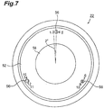
- the respective film thickness measurement points are as shown in Fig. 7.
- measurement points are arranged at a total of 15 portions, i.e., five measurement points 1 to 5 in the vicinity of the position of the first lift pin through hole 56 with respect to it as the measurement point 3, five measurement points 6 to 10 in the vicinity of the position of the second lift pin through hole 56 with respect to it as the measurement point 8, and five measurement points 11 to 15 in the vicinity of the position of the third lift pin through hole 56 with respect to it as the measurement point 13, are arranged clockwise on a circumference passing through the three lift pin through holes 56.
- the distance between any adjacent measurement points in the vicinity of each lift pin through hole 56 is 2° in the angle from the center of the susceptor 22.
- the gap distance d 1 between the wafer W and wafer heating surface 52 is preferably 1 mm or less. If the gap distance is excessively large, the heating efficiency for the wafer W decreases. If the gap distance d 1 is 1 mm or less, excessive decrease in heating efficiency can be prevented. Meanwhile, to suppress a local film thickness change, a certain degree of gap distance is needed. Therefore, a suitable gap distance, e.g., 1 mm, is preferably selected in the above distance range from the conditions for the film thickness.
- the maximum distance from the lower surface of the wafer is set on the basis of a necessary heating efficiency, and a surface with the maximum distance as the gap distance is set. A projection projecting toward the wafer is formed on that portion of this surface where heating is insufficient, thereby forming a wafer heating surface. This can realize adjustment of the heating distribution while maintaining a sufficiently high heating efficiency over the entire portion in the wafer holding area 50. Depending on the heating condition at the respective portions, a recess may be formed in part of the wafer holding area 50.
- the semiconductor manufacturing apparatus is not limited to the embodiment described above, but can be modified in various manners.
- the semiconductor manufacturing apparatus according to the above embodiment is a film deposition apparatus such as an epitaxial growth apparatus
- the present invention can also be applied to other apparatuses for performing other processes, e.g., a CVD apparatus.
- the planar shape within the wafer holding area 50 the three-dimensional structure of the heating adjusting portion may be naturally modified in various manners to match the individual apparatus.
- the wafer support is not also limited to an annular one, as in the above embodiment, which is formed on the entire periphery, but can be stepped or projecting wafer supports formed at a plurality of positions of part of the periphery. A substrate support member other than this may also be used.
- one other than a heating lamp group located below the susceptor may be used.
- the susceptor is formed to form a gap with a predetermined distance between a wafer and a wafer heating surface.
- a heating adjusting portion with a three-dimensional structure is formed on the wafer heating surface to impart a nonconstant distribution to the gap distance.
- This apparatus can be utilized as a semiconductor manufacturing apparatus that can adjust the planar temperature distribution of the wafer and the distribution of the thickness of the formed film by setting the heating conditions such as the heating efficiency distribution of the susceptor for the respective portions of the wafer.
- temperature distribution adjustment when compared to a case wherein temperature distribution is adjusted by means of the heating condition for the susceptor with the lamps, temperature distribution adjustment can be realized more easily and at a lower cost.
- the degree of freedom for adjustment is large and various shape design is possible.
- the temperature distribution uniformity can be sufficiently improved. Since the film deposition pressure need not be decreased, a high film deposition efficiency can be obtained.
Landscapes
- Chemical & Material Sciences (AREA)
- General Chemical & Material Sciences (AREA)
- Chemical Kinetics & Catalysis (AREA)
- Engineering & Computer Science (AREA)
- Materials Engineering (AREA)
- Mechanical Engineering (AREA)
- Metallurgy (AREA)
- Organic Chemistry (AREA)
- Container, Conveyance, Adherence, Positioning, Of Wafer (AREA)
- Chemical Vapour Deposition (AREA)
Abstract
Description
Claims (7)
- A semiconductor manufacturing apparatus comprising a process chamber, a susceptor set in said process chamber to hold a target substrate in a substrate holding area on an upper surface thereof and heat the target substrate, and heating means for heating the target substrate through said susceptor, wherein
said susceptor supports the target substrate with a substrate support member so as to form, in the substrate holding area, a gap with a first distance between a substrate heating surface as that surface portion of the upper surface of said susceptor which opposes the target substrate and a lower surface of the target substrate, and
a heating adjusting portion for forming a gap with a second distance different from the first distance is formed at a predetermined portion on the substrate heating surface. - A semiconductor manufacturing apparatus according to claim 1, wherein
distances of gaps formed at respective portions of the substrate heating surface with respect to the lower surface of the target substrate are not more than the first distance, and
the heating adjusting portion is a projection projecting from the substrate heating surface toward the target substrate. - A semiconductor manufacturing apparatus according to claim 2, wherein the first distance is not more than 1 mm.
- A semiconductor manufacturing apparatus according to claim 1, wherein the substrate support member is a substrate support which is formed on the upper surface of said susceptor along a periphery of the substrate heating surface, and which supports the target substrate when a lower portion of an outer edge of the target substrate comes into contact with an upper surface of the substrate support member.
- A semiconductor manufacturing apparatus according to claim 4, wherein the substrate support is formed annularly in an entire periphery of the substrate heating surface.
- A semiconductor manufacturing apparatus according to claim 1, wherein the heating adjusting portion is formed about a position of rotational center on the substrate heating surface, when said susceptor is rotatably driven, as the center, to be island-like to include the position of rotational center, or annularly and point symmetrically to surround the position of rotational center.
- A semiconductor manufacturing apparatus according to claim 1, wherein said heating means comprises a plurality of heating lamps arranged to oppose a lower surface of said susceptor.
Applications Claiming Priority (3)
| Application Number | Priority Date | Filing Date | Title |
|---|---|---|---|
| JP30954999A JP4592849B2 (en) | 1999-10-29 | 1999-10-29 | Semiconductor manufacturing equipment |
| JP30954999 | 1999-10-29 | ||
| PCT/JP2000/007340 WO2001033617A1 (en) | 1999-10-29 | 2000-10-20 | Semiconductor-manufacturing apparatus |
Publications (3)
| Publication Number | Publication Date |
|---|---|
| EP1235257A1 true EP1235257A1 (en) | 2002-08-28 |
| EP1235257A4 EP1235257A4 (en) | 2002-10-29 |
| EP1235257B1 EP1235257B1 (en) | 2005-08-24 |
Family
ID=17994361
Family Applications (1)
| Application Number | Title | Priority Date | Filing Date |
|---|---|---|---|
| EP00969956A Expired - Lifetime EP1235257B1 (en) | 1999-10-29 | 2000-10-20 | Semiconductor-manufacturing apparatus |
Country Status (7)
| Country | Link |
|---|---|
| US (1) | US7393417B1 (en) |
| EP (1) | EP1235257B1 (en) |
| JP (1) | JP4592849B2 (en) |
| KR (1) | KR20020031417A (en) |
| DE (1) | DE60022221T2 (en) |
| TW (1) | TW460922B (en) |
| WO (1) | WO2001033617A1 (en) |
Cited By (2)
| Publication number | Priority date | Publication date | Assignee | Title |
|---|---|---|---|---|
| WO2006012048A3 (en) * | 2004-06-29 | 2006-09-28 | Intel Corp | Deposition apparatus for providing uniform low-k dielectric |
| US7785419B2 (en) | 2005-12-27 | 2010-08-31 | Sumco Corporation | Epitaxial apparatus |
Families Citing this family (42)
| Publication number | Priority date | Publication date | Assignee | Title |
|---|---|---|---|---|
| JP4137407B2 (en) * | 2001-05-21 | 2008-08-20 | 日本オプネクスト株式会社 | Manufacturing method of optical semiconductor device |
| JP2003086890A (en) * | 2001-09-11 | 2003-03-20 | Oki Electric Ind Co Ltd | Method of manufacturing semiconductor light emitting element |
| KR100443122B1 (en) * | 2001-10-19 | 2004-08-04 | 삼성전자주식회사 | Heater Assembly for Fabricating a Semiconductor Device |
| AU2003287837A1 (en) | 2002-12-20 | 2004-07-14 | Vortek Industries Ltd | Methods and systems for supporting a workpiece and for heat-treating the workpiece |
| WO2005013334A2 (en) * | 2003-08-01 | 2005-02-10 | Sgl Carbon Ag | Holder for supporting wafers during semiconductor manufacture |
| TW200711029A (en) * | 2005-08-05 | 2007-03-16 | Tokyo Electron Ltd | Substrate processing apparatus and substrate stage used therein |
| KR100811389B1 (en) * | 2006-03-24 | 2008-03-07 | 가부시키가이샤 뉴플레어 테크놀로지 | Semiconductor manufacturing equipment and heater |
| JP5967859B2 (en) * | 2006-11-15 | 2016-08-10 | マトソン テクノロジー、インコーポレイテッド | System and method for supporting a workpiece during heat treatment |
| US20080314319A1 (en) * | 2007-06-19 | 2008-12-25 | Memc Electronic Materials, Inc. | Susceptor for improving throughput and reducing wafer damage |
| JP2009038294A (en) * | 2007-08-03 | 2009-02-19 | Shin Etsu Handotai Co Ltd | Output adjustment method, silicon epitaxial wafer manufacturing method, and susceptor |
| JP5444607B2 (en) * | 2007-10-31 | 2014-03-19 | 株式会社Sumco | Epitaxial film forming apparatus susceptor, epitaxial film forming apparatus, and epitaxial wafer manufacturing method |
| US8404049B2 (en) * | 2007-12-27 | 2013-03-26 | Memc Electronic Materials, Inc. | Epitaxial barrel susceptor having improved thickness uniformity |
| JP2009270143A (en) | 2008-05-02 | 2009-11-19 | Nuflare Technology Inc | Susceptor, semiconductor manufacturing apparatus, and semiconductor method for manufacturing |
| WO2009137940A1 (en) | 2008-05-16 | 2009-11-19 | Mattson Technology Canada, Inc. | Workpiece breakage prevention method and apparatus |
| US8042697B2 (en) * | 2008-06-30 | 2011-10-25 | Memc Electronic Materials, Inc. | Low thermal mass semiconductor wafer support |
| JP5200171B2 (en) * | 2008-08-29 | 2013-05-15 | ビーコ・インストゥルメンツ・インコーポレイテッド | Wafer carrier, chemical vapor deposition apparatus, and method of processing wafer |
| US20100098519A1 (en) * | 2008-10-17 | 2010-04-22 | Memc Electronic Materials, Inc. | Support for a semiconductor wafer in a high temperature environment |
| JP5184302B2 (en) * | 2008-11-04 | 2013-04-17 | Sumco Techxiv株式会社 | Susceptor device, epitaxial wafer manufacturing apparatus, and epitaxial wafer manufacturing method |
| US8129284B2 (en) | 2009-04-28 | 2012-03-06 | Dainippon Screen Mfg. Co., Ltd. | Heat treatment method and heat treatment apparatus for heating substrate by light irradiation |
| JP5620114B2 (en) * | 2010-01-29 | 2014-11-05 | 大日本スクリーン製造株式会社 | Heat treatment method and heat treatment apparatus |
| JP5869899B2 (en) * | 2011-04-01 | 2016-02-24 | 株式会社日立国際電気 | Substrate processing apparatus, semiconductor device manufacturing method, substrate processing method, and susceptor cover |
| KR20130111029A (en) * | 2012-03-30 | 2013-10-10 | 삼성전자주식회사 | Susceptor for chemical vapor deposition apparatus and chemical vapor deposition apparatus having the same |
| US10316412B2 (en) | 2012-04-18 | 2019-06-11 | Veeco Instruments Inc. | Wafter carrier for chemical vapor deposition systems |
| US9401271B2 (en) | 2012-04-19 | 2016-07-26 | Sunedison Semiconductor Limited (Uen201334164H) | Susceptor assemblies for supporting wafers in a reactor apparatus |
| US10167571B2 (en) | 2013-03-15 | 2019-01-01 | Veeco Instruments Inc. | Wafer carrier having provisions for improving heating uniformity in chemical vapor deposition systems |
| WO2014143499A1 (en) * | 2013-03-15 | 2014-09-18 | Applied Materials, Inc. | Susceptor support shaft with uniformity tuning lenses for epi process |
| TWI609991B (en) * | 2013-06-05 | 2018-01-01 | 維克儀器公司 | Improved wafer carrier having thermal uniformity-enhancing features |
| CN103456672B (en) * | 2013-09-04 | 2016-03-09 | 沈阳拓荆科技有限公司 | Open pin support plate |
| JP6189164B2 (en) * | 2013-09-30 | 2017-08-30 | 住友電工デバイス・イノベーション株式会社 | Growth equipment |
| US10658222B2 (en) | 2015-01-16 | 2020-05-19 | Lam Research Corporation | Moveable edge coupling ring for edge process control during semiconductor wafer processing |
| US20170032992A1 (en) * | 2015-07-31 | 2017-02-02 | Infineon Technologies Ag | Substrate carrier, a method and a processing device |
| US10770336B2 (en) * | 2017-08-08 | 2020-09-08 | Asm Ip Holding B.V. | Substrate lift mechanism and reactor including same |
| JP6878212B2 (en) * | 2017-09-07 | 2021-05-26 | 昭和電工株式会社 | Manufacturing method for susceptors, CVD equipment and epitaxial wafers |
| WO2019103722A1 (en) | 2017-11-21 | 2019-05-31 | Lam Research Corporation | Bottom and middle edge rings |
| CN108962782B (en) * | 2018-04-28 | 2025-02-14 | 北京艾姆希半导体科技有限公司 | Chip heating device and method for manufacturing chip heating device |
| CN118398464A (en) | 2018-08-13 | 2024-07-26 | 朗姆研究公司 | Replaceable and/or collapsible edge ring assembly incorporating edge ring positioning and centering functions for plasma sheath adjustment |
| CN112420591B (en) * | 2019-08-20 | 2022-06-10 | 长鑫存储技术有限公司 | Heating plate and method for controlling surface temperature of wafer |
| CN112786547B (en) * | 2019-11-01 | 2023-10-13 | 神讯电脑(昆山)有限公司 | Thermal architecture |
| WO2021120189A1 (en) * | 2019-12-20 | 2021-06-24 | 苏州晶湛半导体有限公司 | Wafer susceptor and chemical vapor deposition equipment |
| CN115315775A (en) | 2020-03-23 | 2022-11-08 | 朗姆研究公司 | Medium ring corrosion compensation in substrate processing systems |
| CN113818003A (en) * | 2020-06-19 | 2021-12-21 | 拓荆科技股份有限公司 | A kind of film preparation method and equipment |
| CN116349002A (en) | 2020-10-05 | 2023-06-27 | 朗姆研究公司 | Removable Edge Ring for Plasma Processing Systems |
Family Cites Families (18)
| Publication number | Priority date | Publication date | Assignee | Title |
|---|---|---|---|---|
| US5242501A (en) * | 1982-09-10 | 1993-09-07 | Lam Research Corporation | Susceptor in chemical vapor deposition reactors |
| JPS61215289A (en) * | 1985-03-19 | 1986-09-25 | Toshiba Mach Co Ltd | Vapor-phase growth apparatus |
| JPS61288416A (en) * | 1985-06-17 | 1986-12-18 | Toshiba Corp | Susceptor for heating of semiconductor substrate |
| JPS624315A (en) * | 1985-06-29 | 1987-01-10 | Toshiba Corp | Susceptor for vapor growth apparatus |
| JPS6242416A (en) * | 1985-08-19 | 1987-02-24 | Toshiba Corp | Susceptor for heating semiconductor substrate |
| EP0448346B1 (en) * | 1990-03-19 | 1997-07-09 | Kabushiki Kaisha Toshiba | Vapor-phase deposition apparatus |
| JPH0610140A (en) * | 1992-06-24 | 1994-01-18 | Fuji Film Micro Device Kk | Thin film deposition device |
| JPH0758041A (en) * | 1993-08-20 | 1995-03-03 | Toshiba Ceramics Co Ltd | Susceptor |
| JP3004846B2 (en) * | 1993-08-20 | 2000-01-31 | 東芝セラミックス株式会社 | Susceptor for vapor phase growth equipment |
| DE69424759T2 (en) * | 1993-12-28 | 2001-02-08 | Applied Materials, Inc. | Vapor deposition process in a single chamber for thin film transistors |
| US5645646A (en) * | 1994-02-25 | 1997-07-08 | Applied Materials, Inc. | Susceptor for deposition apparatus |
| US5493987A (en) * | 1994-05-16 | 1996-02-27 | Ag Associates, Inc. | Chemical vapor deposition reactor and method |
| JPH0936049A (en) | 1995-07-21 | 1997-02-07 | Mitsubishi Electric Corp | Vapor growth apparatus and compound semiconductor device manufactured by the same |
| JPH09181155A (en) * | 1995-09-29 | 1997-07-11 | Applied Materials Inc | Deposition equipment susceptor |
| JP3665672B2 (en) * | 1995-11-01 | 2005-06-29 | 東京エレクトロン株式会社 | Film forming apparatus and film forming method |
| JP3467960B2 (en) * | 1996-02-29 | 2003-11-17 | 信越半導体株式会社 | Method and apparatus for producing semiconductor single crystal thin film |
| JP3891636B2 (en) * | 1997-04-22 | 2007-03-14 | 株式会社ルネサステクノロジ | Semiconductor manufacturing apparatus and semiconductor wafer transfer method |
| JP3440769B2 (en) * | 1997-06-30 | 2003-08-25 | 三菱住友シリコン株式会社 | Wafer adapter |
-
1999
- 1999-10-29 JP JP30954999A patent/JP4592849B2/en not_active Expired - Lifetime
-
2000
- 2000-10-20 US US10/111,555 patent/US7393417B1/en not_active Expired - Lifetime
- 2000-10-20 KR KR1020027002513A patent/KR20020031417A/en not_active Ceased
- 2000-10-20 EP EP00969956A patent/EP1235257B1/en not_active Expired - Lifetime
- 2000-10-20 WO PCT/JP2000/007340 patent/WO2001033617A1/en not_active Ceased
- 2000-10-20 DE DE60022221T patent/DE60022221T2/en not_active Expired - Fee Related
- 2000-10-26 TW TW089122599A patent/TW460922B/en not_active IP Right Cessation
Cited By (2)
| Publication number | Priority date | Publication date | Assignee | Title |
|---|---|---|---|---|
| WO2006012048A3 (en) * | 2004-06-29 | 2006-09-28 | Intel Corp | Deposition apparatus for providing uniform low-k dielectric |
| US7785419B2 (en) | 2005-12-27 | 2010-08-31 | Sumco Corporation | Epitaxial apparatus |
Also Published As
| Publication number | Publication date |
|---|---|
| JP4592849B2 (en) | 2010-12-08 |
| US7393417B1 (en) | 2008-07-01 |
| KR20020031417A (en) | 2002-05-01 |
| TW460922B (en) | 2001-10-21 |
| EP1235257B1 (en) | 2005-08-24 |
| EP1235257A4 (en) | 2002-10-29 |
| WO2001033617A1 (en) | 2001-05-10 |
| JP2001126995A (en) | 2001-05-11 |
| DE60022221D1 (en) | 2005-09-29 |
| DE60022221T2 (en) | 2006-06-22 |
Similar Documents
| Publication | Publication Date | Title |
|---|---|---|
| EP1235257B1 (en) | Semiconductor-manufacturing apparatus | |
| CN110494957B (en) | Epitaxial growth device, preheat ring, and method for manufacturing epitaxial wafer using these | |
| US9096949B2 (en) | Susceptor support portion and epitaxial growth apparatus including susceptor support portion | |
| US10513797B2 (en) | Manufacturing method of epitaxial silicon wafer | |
| KR20060060735A (en) | Silicon epitaxial wafer manufacturing method and silicon epitaxial wafer | |
| WO2007091638A1 (en) | Susceptor and apparatus for manufacturing epitaxial wafer | |
| JP4300523B2 (en) | Epitaxial growth equipment | |
| KR20020026480A (en) | Wafer supporting device of semiconductor manufacturing device | |
| CN113604871B (en) | Base support frame, device and method for epitaxial growth of silicon wafer | |
| TWI706446B (en) | Epitaxial growth device and method for manufacturing epitaxial wafer using the same | |
| US7060944B2 (en) | Heat treatment device and heat treatment method | |
| US6971835B2 (en) | Vapor-phase epitaxial growth method | |
| KR20010080247A (en) | Wafer support of semiconductor manufacturing system | |
| JP2002151412A (en) | Semiconductor manufacturing equipment | |
| US12519005B2 (en) | Thickness uniformity improvement kit for thermally sensitive epitaxial processing | |
| JP2012004148A (en) | Position adjusting method of internal member in epitaxial growth device | |
| CN116555904A (en) | A base and device for silicon wafer epitaxial growth | |
| TWI867238B (en) | Window for chemical vapor deposition systems and related methods | |
| JP3357311B2 (en) | Wafer support device in semiconductor manufacturing equipment | |
| JP2001010894A (en) | Susceptor for crystal growth and crystal growth device, and epitaxial wafer and its production | |
| KR20230138547A (en) | Flat pocket susceptor design for improved heat transfer | |
| JP4868503B2 (en) | Epitaxial wafer manufacturing method | |
| JP2006041028A (en) | Susceptor and epitaxial wafer manufacturing method | |
| US20060185596A1 (en) | Vapor phase growth method by controlling the heat output in the gas introduction region | |
| EP3305940A1 (en) | Susceptor |
Legal Events
| Date | Code | Title | Description |
|---|---|---|---|
| PUAI | Public reference made under article 153(3) epc to a published international application that has entered the european phase |
Free format text: ORIGINAL CODE: 0009012 |
|
| 17P | Request for examination filed |
Effective date: 20020528 |
|
| AK | Designated contracting states |
Kind code of ref document: A1 Designated state(s): AT BE CH CY DE DK ES FI FR GB GR IE IT LI LU MC NL PT SE |
|
| A4 | Supplementary search report drawn up and despatched | ||
| AK | Designated contracting states |
Kind code of ref document: A4 Designated state(s): AT BE CH CY DE DK ES FI FR GB GR IE IT LI LU MC NL PT SE |
|
| A4 | Supplementary search report drawn up and despatched |
Effective date: 20021029 |
|
| RIC1 | Information provided on ipc code assigned before grant |
Free format text: 7H 01L 21/205 A, 7H 01L 21/68 B, 7H 01L 21/00 B, 7C 23C 16/48 B, 7C 23C 16/458 B, 7C 23C 16/46 B |
|
| 17Q | First examination report despatched |
Effective date: 20030331 |
|
| RBV | Designated contracting states (corrected) |
Designated state(s): AT BE DE FR |
|
| RBV | Designated contracting states (corrected) |
Designated state(s): DE FR |
|
| GRAP | Despatch of communication of intention to grant a patent |
Free format text: ORIGINAL CODE: EPIDOSNIGR1 |
|
| GRAS | Grant fee paid |
Free format text: ORIGINAL CODE: EPIDOSNIGR3 |
|
| GRAA | (expected) grant |
Free format text: ORIGINAL CODE: 0009210 |
|
| AK | Designated contracting states |
Kind code of ref document: B1 Designated state(s): DE FR |
|
| REF | Corresponds to: |
Ref document number: 60022221 Country of ref document: DE Date of ref document: 20050929 Kind code of ref document: P |
|
| PLBE | No opposition filed within time limit |
Free format text: ORIGINAL CODE: 0009261 |
|
| STAA | Information on the status of an ep patent application or granted ep patent |
Free format text: STATUS: NO OPPOSITION FILED WITHIN TIME LIMIT |
|
| 26N | No opposition filed |
Effective date: 20060526 |
|
| EN | Fr: translation not filed | ||
| PG25 | Lapsed in a contracting state [announced via postgrant information from national office to epo] |
Ref country code: FR Free format text: LAPSE BECAUSE OF FAILURE TO SUBMIT A TRANSLATION OF THE DESCRIPTION OR TO PAY THE FEE WITHIN THE PRESCRIBED TIME-LIMIT Effective date: 20061020 |
|
| PG25 | Lapsed in a contracting state [announced via postgrant information from national office to epo] |
Ref country code: FR Free format text: LAPSE BECAUSE OF FAILURE TO SUBMIT A TRANSLATION OF THE DESCRIPTION OR TO PAY THE FEE WITHIN THE PRESCRIBED TIME-LIMIT Effective date: 20051031 |
|
| PG25 | Lapsed in a contracting state [announced via postgrant information from national office to epo] |
Ref country code: FR Free format text: LAPSE BECAUSE OF FAILURE TO SUBMIT A TRANSLATION OF THE DESCRIPTION OR TO PAY THE FEE WITHIN THE PRESCRIBED TIME-LIMIT Effective date: 20050824 |
|
| PGFP | Annual fee paid to national office [announced via postgrant information from national office to epo] |
Ref country code: DE Payment date: 20081031 Year of fee payment: 9 |
|
| PG25 | Lapsed in a contracting state [announced via postgrant information from national office to epo] |
Ref country code: DE Free format text: LAPSE BECAUSE OF NON-PAYMENT OF DUE FEES Effective date: 20100501 |