EP1233516A2 - Logikschaltung, insbesondere für eisenbahntechnische Anlagen - Google Patents
Logikschaltung, insbesondere für eisenbahntechnische Anlagen Download PDFInfo
- Publication number
- EP1233516A2 EP1233516A2 EP02002870A EP02002870A EP1233516A2 EP 1233516 A2 EP1233516 A2 EP 1233516A2 EP 02002870 A EP02002870 A EP 02002870A EP 02002870 A EP02002870 A EP 02002870A EP 1233516 A2 EP1233516 A2 EP 1233516A2
- Authority
- EP
- European Patent Office
- Prior art keywords
- components
- data
- component
- logic circuit
- programmed
- Prior art date
- Legal status (The legal status is an assumption and is not a legal conclusion. Google has not performed a legal analysis and makes no representation as to the accuracy of the status listed.)
- Granted
Links
Images


Classifications
-
- H—ELECTRICITY
- H03—ELECTRONIC CIRCUITRY
- H03K—PULSE TECHNIQUE
- H03K19/00—Logic circuits, i.e. having at least two inputs acting on one output; Inverting circuits
- H03K19/007—Fail-safe circuits
Definitions
- the present invention relates to a logic circuit according to the preamble of claim 1.
- the present invention is therefore based on the object to specify a logic circuit in which two of the same and identically programmed logic modules the same program regardless of the logic module used and the one used Programming system runs in the two copies, and still the residual probability of a double error due to a systematic error on a particular Place on the chip converged to zero.
- Fig. 1 shows a redundant logic circuit 10, each in a partial circuit (as such not shown in Fig. 1) is structured with an associated component 1 and 1 '.
- the components 1 and 1 ' are preferably FPGA components executed These components 1, 1 'are on the Pins 31 to an environment, e.g. a printed circuit board.
- A1 and A2 A area abstract zones are open designated the two components 1, 1 ', the predetermined Include data and programmed functions.
- VHDL V ery High Speed H ardware D escription L anguage IEEE 1087-1987 / 1993
- Combinatorial logic modules such as gate elements with the functions AND, NAND, OR, flip / flops, counters, decoders etc. are available for this.
- storage logic modules which can contain, for example, an address, a maximum value or a text in ASCII (American Standard Code for Information Interchange) in an arrangement.
- ASCII American Standard Code for Information Interchange
- further requirements such as, for example, compliance with the maximum predetermined signal propagation times, can be taken into account by placing the functional areas required for this as close as possible, in particular to a corner of the component.
- the quality of the desired local separation of the functional areas can be checked with the usually available layout editor.
- the circuit is constructed so that there is always at least two identical copies of the logic circuits in each component 1 and 1 'can be programmed.
- One is the Part A1 with the connection zones 311 used in the other Copy part A2 is used with the connection zone 312.
- These connections refer to the exchange of data and the mutual monitoring of two components, but not on the data connections outside
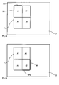
- FIGS. 2a and 2b show a further embodiment of the Present invention illustrated the presence of enough logic and connection capacity an even better one Allows separation of active systems.
- Fig. 2a shows one first subcircuit 11 and FIG. 2b a second subcircuit 12.
- the two subcircuits 11 and 12 each have an identical one Component 1 and 1 'and form the double redundant Parts of a logic circuit.
- Embedding the Subcircuits 11 and 12 in the logic circuit can be on different, local, mechanical and electrical ways and is in connection with the present invention not continued. All logic in everyone Component 1 and 1 'is functional four times in four identical Areas - also called copies - A1, A2, A3 and A4 programmed.
- a further embodiment of the present invention are not required logic functions, namely combinatorial and storing with a "fill logic" called here Function occupied.
- the two above-mentioned are particularly preferred Arrange types of logic modules alternately and only input 31 (input pin) to be specified.
- the Connections on the circuit board side to the named Input pins are to be placed electrically to ground internal to the component as well as on the side of the circuit board Interferences such as coupling or radiation / decoupling switch off if possible.
- One is particularly useful Flat design of the connections to the input pins.
- This Fill logic is preferably designed multiple times, one basic arrangement is shown in Fig. 2c, the Areas corresponding to filling logic are identified by the reference symbol N1 provided.
- the present invention is not on FPGA device families limited.
- the invention based on a memory layout electrically programmable component, which preferably is implemented as a flash EPROM.
- FIG. 3 is a word organized and byte addressable Memory 2 shown.
- the organization of this storage 2 amount to n x 1 word, one word being defined as 16 bits and the lower and upper part of a word also individually are addressable, e.g. with address line A0 (not shown in Fig. 3).
- the bit positions are in FIG. 3 from right to left with 0 .. 7 and 8 .. 15 in decimal representation designated. With 0 .. 15 or 32 .. 47 are in the Fig. 3 denotes addresses of half words; the specified Addresses are only exemplary, in particular do not need the identically programmed areas on the Component address 0 to start. To avoid double errors, the data is also multiple in the memory layout provided.
- areas are identical data included labeled D1.
- areas are identical data included labeled D1.
- the different areas not exactly To set addresses that correspond to a power of two.
- the FPGA component 1 always accesses the low-order half of the word memory 2, while the FPGA device in the second subcircuit 12 always on the higher order half of the word memory accesses.
- 3 are not shown FPGA components 1, which are coupled to one another. About such a coupling can be obtained from the memory 2 from different Areas originating and across different Lines transferred to the relevant FPGA component 1 Data checked for equality, especially integrity become.
- data is used in connection with the present Invention also understood code for a processor system.
- code is so-called position-independent is, i.e. regardless of its location in the address space is executable.
Landscapes
- Physics & Mathematics (AREA)
- Engineering & Computer Science (AREA)
- Computer Hardware Design (AREA)
- Computing Systems (AREA)
- General Engineering & Computer Science (AREA)
- Mathematical Physics (AREA)
- Logic Circuits (AREA)
- Train Traffic Observation, Control, And Security (AREA)
- Design And Manufacture Of Integrated Circuits (AREA)
- Electric Propulsion And Braking For Vehicles (AREA)
- Safety Devices In Control Systems (AREA)
Abstract
Description
können sind die beiden Datenbereiche funktionell und elektrisch sicher getrennt (Patentanspruch 2).
können diese gemeinsam flächig auf Masse gelegt werden und reduzieren dadurch die induktive Abstrahlung und die Einkopplung (Patentanspruch 3).
- Figur 1
- Ausführungsform einer redundanten Logikschaltung mit zwei Bauelementen bei zweifach identischer Programmierung einschliesslich der Darstellung der Kontaktierung ;
- Figur 2a
- Ausführungsform einer ersten Teilschaltung mit vier identischen Programmierungen, wobei nur eine Programmierung verwendet wird, zusammen mit den entsprechenden aktiven Anschlusszonen für das Bauelement;
- Figur 2b
- Ausführungsform einer zweiten Teilschaltung mit vier identischen Programmierungen, wobei nur eine Programmierung verwendet wird, zusammen mit den entsprechenden aktiven Anschlusszonen für das Bauelement;
- Figur 2c
- Prinzipdarstellung des Layouts eines Bauelementes mit einer Füll-Logik;
- Figur 3
- Speicherlayout eines Speicherbauelementes mit mehreren identisch programmierten Bereichen.
- 1, 1'
- Bauelement, vorzugsweise FPGA
- 2
- Bauelement, vorzugsweise Flash-PROM oder EPROM
- 5
- Abstrakte Trennungslinie
- 10
- Logikschaltung
- 11
- Erste Teilschaltung einer redundant ausgeführten Logikschaltung
- 12
- Zweite Teilschaltung einer redundant ausgeführten Logikschaltung
- 31
- Bauelement-Anschluss, Pin
- 311, 312
- Anschlusszonen der Bauelemente 1, 1'
- 331, 332
- Anschlusszonen zum funktionalen Bereich A1 auf dem Bauelement 1
- 341, 342
- Anschlusszonen zum funktionalen Bereich A2 auf dem Bauelement 1'
- A1, A2, A3, A4
- funktionale Bereiche auf dem Bauelement 1
- N1
- Füll-Logik-Bereich auf den Bauelementen 1, 1'
- D1
- Datenbereich auf den Bauelementen 1, 1'
Claims (7)
- Logikschaltung, die wenigstens in zwei redundante Teilschaltungen (11, 12) gegliedert ist, die wenigstens je ein identisches und mit Daten programmierbares Bauelement (1, 1') aufweisen,
dadurch gekennzeichnet, dass
in den je identischen Bauelementen (1, 1') die Daten (D1) wenigstens zweifach identisch programmiert enthalten sind (A1, A2) und dass die identischen Bauelemente (1, 1') an die jeweils zugehörige Teilschaltung (11, 12) verschieden angeschlossen (311, 312; 331, 332; 341, 342) sind. - Logikschaltung nach Anspruch 1,
dadurch gekennzeichnet, dass
in den je identischen Bauelementen (1, 1') die wenigstens zweifach identisch programmierten Daten (D1) durch wenigstens einen Bereich (N1) getrennt sind, der eine Füll-Logik beinhaltet. - Logikschaltung nach Anspruch 2,
dadurch gekennzeichnet, dass
der die Füll-Logik beinhaltende Bereich (N1) nur als Eingang benutzbare Bauelementanschlüsse (31) aufweist. - Logikschaltung nach einem der Ansprüche 1 bis 3,
dadurch gekennzeichnet, dass
die je identischen Bauelemente (1, 1') mit einem weiteren mit Daten programmierbaren Bauelement (2) verbunden sind, das mehrere mit identischen Daten (D1) programmierte Bereiche aufweist und wobei von jedem identischen Bauelement (1, 1') das weitere Bauelement (2) verschieden adressierbar ist. - Logikschaltung, nach Anspruch 4,
dadurch gekennzeichnet, dass
in dem weiteren Bauelement (2) die mit identischen Daten (D1) programmierten Bereiche an Adressen liegen, die ungleich einer Zweierpotenz sind. - Logikschaltung nach Anspruch 5,
dadurch gekennzeichnet, dass
das weitere Bauelement (2) neben den mit identischen Daten (D1) programmierten Bereichen weitere Bereiche aufweist, die feste Daten oder eine Prüfsumme enthalten. - Logikschaltung nach einem der Ansprüche 4 bis 6,
dadurch gekennzeichnet, dass
die identisch programmierten Bauelemente (1, 1') gekoppelt sind und dass die aus dem weiteren Bauelement (2) entstammenden Daten über diese Kopplung auf Integrität prüfbar sind.
Priority Applications (2)
| Application Number | Priority Date | Filing Date | Title |
|---|---|---|---|
| EP02002870A EP1233516B1 (de) | 2001-02-15 | 2002-02-08 | Logikschaltung, insbesondere für eisenbahntechnische Anlagen |
| CY20071100406T CY1106410T1 (el) | 2001-02-15 | 2007-03-22 | Λογικο κυκλωμα, ιδιαιτepα για σιδηροδρομικες εγκαταστασεις |
Applications Claiming Priority (3)
| Application Number | Priority Date | Filing Date | Title |
|---|---|---|---|
| EP01103494 | 2001-02-15 | ||
| EP01103494 | 2001-02-15 | ||
| EP02002870A EP1233516B1 (de) | 2001-02-15 | 2002-02-08 | Logikschaltung, insbesondere für eisenbahntechnische Anlagen |
Publications (3)
| Publication Number | Publication Date |
|---|---|
| EP1233516A2 true EP1233516A2 (de) | 2002-08-21 |
| EP1233516A3 EP1233516A3 (de) | 2004-03-31 |
| EP1233516B1 EP1233516B1 (de) | 2007-01-24 |
Family
ID=37728489
Family Applications (1)
| Application Number | Title | Priority Date | Filing Date |
|---|---|---|---|
| EP02002870A Expired - Lifetime EP1233516B1 (de) | 2001-02-15 | 2002-02-08 | Logikschaltung, insbesondere für eisenbahntechnische Anlagen |
Country Status (7)
| Country | Link |
|---|---|
| EP (1) | EP1233516B1 (de) |
| AT (1) | ATE352903T1 (de) |
| CY (1) | CY1106410T1 (de) |
| DE (1) | DE50209316D1 (de) |
| DK (1) | DK1233516T3 (de) |
| ES (1) | ES2276862T3 (de) |
| PT (1) | PT1233516E (de) |
Families Citing this family (1)
| Publication number | Priority date | Publication date | Assignee | Title |
|---|---|---|---|---|
| DE102023109028B3 (de) | 2023-04-11 | 2024-10-10 | Scheidt & Bachmann Gmbh | Prüfschaltungsanordnung |
Family Cites Families (2)
| Publication number | Priority date | Publication date | Assignee | Title |
|---|---|---|---|---|
| US7284152B1 (en) * | 1997-02-26 | 2007-10-16 | Siemens Aktiengesellschaft | Redundancy-based electronic device having certified and non-certified channels |
| DE19805819B4 (de) * | 1997-05-06 | 2006-11-23 | Ee-Signals Gmbh & Co. Kg | Verfahren zur Überwachung von integrierten Schaltkreisen |
-
2002
- 2002-02-08 ES ES02002870T patent/ES2276862T3/es not_active Expired - Lifetime
- 2002-02-08 DE DE50209316T patent/DE50209316D1/de not_active Expired - Lifetime
- 2002-02-08 AT AT02002870T patent/ATE352903T1/de active
- 2002-02-08 DK DK02002870T patent/DK1233516T3/da active
- 2002-02-08 PT PT02002870T patent/PT1233516E/pt unknown
- 2002-02-08 EP EP02002870A patent/EP1233516B1/de not_active Expired - Lifetime
-
2007
- 2007-03-22 CY CY20071100406T patent/CY1106410T1/el unknown
Also Published As
| Publication number | Publication date |
|---|---|
| EP1233516A3 (de) | 2004-03-31 |
| EP1233516B1 (de) | 2007-01-24 |
| DE50209316D1 (de) | 2007-03-15 |
| PT1233516E (pt) | 2007-02-28 |
| DK1233516T3 (da) | 2007-05-29 |
| ATE352903T1 (de) | 2007-02-15 |
| CY1106410T1 (el) | 2011-10-12 |
| ES2276862T3 (es) | 2007-07-01 |
Similar Documents
| Publication | Publication Date | Title |
|---|---|---|
| DE69620022T2 (de) | Laser-sicherungsbankstruktur | |
| DE69027030T2 (de) | Eine fehlertolerante datenspeicherungsanordnung | |
| EP0049322B1 (de) | Auslesesicherung bei Einchip-Mikroprozessoren | |
| DE69719479T2 (de) | Datenverarbeitungssystemsicherheit | |
| DE3048365C2 (de) | ||
| DE69815258T2 (de) | Elektrisch programmier- und löschbarer nichtflüchtiger Speicher mit einem lese- und/oder schreibgeschützen Bereich einschliesslich zugehöriger elektronischer Schaltung | |
| DE3128740C2 (de) | ||
| DE2225841C3 (de) | Verfahren und Anordnung zur systematischen Fehlerprüfung eines monolithischen Halbleiterspeichers | |
| DE2328869A1 (de) | Verfahren zur pruefung eines digitalen speichersystems sowie zur durchfuehrung dieses verfahrens dienendes selbstpruefendes digitales speichersystem | |
| DE2646162B2 (de) | Schaltungsanordnung zum Ersetzen fehlerhafter Informationen in Speicherplätzen eines nicht veränderbaren Speichers | |
| DE2350146A1 (de) | Verfahren und netzwerk zur neuordnung eines rechnerspeichersystems | |
| DE2721599A1 (de) | Verfahren und geraet zur verhinderung der ausgabe von fehlerhaften daten in digitalen datenverarbeitungseinrichtungen | |
| DE102007058928A1 (de) | Verfahren und Halbleiterspeicher mit einer Einrichtung zur Erkennung von Adressierungsfehlern | |
| DE2926322A1 (de) | Speicher-subsystem | |
| DE102004012279B3 (de) | Verfahren und Vorrichtung zum Speicherselbsttest von eingebetteten Speichern in Halbleiterchips | |
| DE10058030A1 (de) | Integrierte Schaltung mit Datenprüfmitteln auf einem Chip | |
| EP0276450A1 (de) | Datenschutzschaltung zur Sperrung der Uebertragung von Signalen über einen Bus | |
| EP1205938A2 (de) | Integrierte Schaltung mit Testbetriebsart und Verfahren zum Testen einer Vielzahl solcher integrierter Schaltungen | |
| DE4429764C2 (de) | Zeitgebereinrichtung für einen Mikrocomputer | |
| DE3327874A1 (de) | Speichermodul fuer ein programmierbares elektronisches geraet | |
| EP1233516B1 (de) | Logikschaltung, insbesondere für eisenbahntechnische Anlagen | |
| EP1254461B1 (de) | Testbarer festwertspeicher für datenspeicher-redundanzlogik | |
| EP1924916A2 (de) | Speicheranordnung und betriebsverfahren dafür | |
| DE10134090A1 (de) | Speicher und Verfahren zum Ersetzen von fehlerhaften Speicherzellen in demselben | |
| DE3855174T2 (de) | Selbstprüfung der Paritätsregenerierung |
Legal Events
| Date | Code | Title | Description |
|---|---|---|---|
| PUAI | Public reference made under article 153(3) epc to a published international application that has entered the european phase |
Free format text: ORIGINAL CODE: 0009012 |
|
| AK | Designated contracting states |
Kind code of ref document: A2 Designated state(s): AT BE CH CY DE DK ES FI FR GB GR IE IT LI LU MC NL PT SE TR |
|
| AX | Request for extension of the european patent |
Free format text: AL;LT;LV;MK;RO;SI |
|
| PUAL | Search report despatched |
Free format text: ORIGINAL CODE: 0009013 |
|
| AK | Designated contracting states |
Kind code of ref document: A3 Designated state(s): AT BE CH CY DE DK ES FI FR GB GR IE IT LI LU MC NL PT SE TR |
|
| AX | Request for extension of the european patent |
Extension state: AL LT LV MK RO SI |
|
| 17P | Request for examination filed |
Effective date: 20040308 |
|
| AKX | Designation fees paid |
Designated state(s): AT BE CH CY DE DK ES FI FR GB GR IE IT LI LU MC NL PT SE TR |
|
| GRAP | Despatch of communication of intention to grant a patent |
Free format text: ORIGINAL CODE: EPIDOSNIGR1 |
|
| GRAS | Grant fee paid |
Free format text: ORIGINAL CODE: EPIDOSNIGR3 |
|
| GRAA | (expected) grant |
Free format text: ORIGINAL CODE: 0009210 |
|
| AK | Designated contracting states |
Kind code of ref document: B1 Designated state(s): AT BE CH CY DE DK ES FI FR GB GR IE IT LI LU MC NL PT SE TR |
|
| REG | Reference to a national code |
Ref country code: GB Ref legal event code: FG4D Free format text: NOT ENGLISH |
|
| REG | Reference to a national code |
Ref country code: CH Ref legal event code: EP |
|
| PG25 | Lapsed in a contracting state [announced via postgrant information from national office to epo] |
Ref country code: MC Free format text: LAPSE BECAUSE OF NON-PAYMENT OF DUE FEES Effective date: 20070228 |
|
| REG | Reference to a national code |
Ref country code: PT Ref legal event code: SC4A Free format text: AVAILABILITY OF NATIONAL TRANSLATION Effective date: 20070213 |
|
| REG | Reference to a national code |
Ref country code: IE Ref legal event code: FG4D Free format text: LANGUAGE OF EP DOCUMENT: GERMAN |
|
| GBT | Gb: translation of ep patent filed (gb section 77(6)(a)/1977) |
Effective date: 20070219 |
|
| REF | Corresponds to: |
Ref document number: 50209316 Country of ref document: DE Date of ref document: 20070315 Kind code of ref document: P |
|
| REG | Reference to a national code |
Ref country code: GR Ref legal event code: EP Ref document number: 20070400909 Country of ref document: GR |
|
| REG | Reference to a national code |
Ref country code: SE Ref legal event code: TRGR |
|
| REG | Reference to a national code |
Ref country code: DK Ref legal event code: T3 |
|
| REG | Reference to a national code |
Ref country code: ES Ref legal event code: FG2A Ref document number: 2276862 Country of ref document: ES Kind code of ref document: T3 |
|
| ET | Fr: translation filed | ||
| PLBE | No opposition filed within time limit |
Free format text: ORIGINAL CODE: 0009261 |
|
| STAA | Information on the status of an ep patent application or granted ep patent |
Free format text: STATUS: NO OPPOSITION FILED WITHIN TIME LIMIT |
|
| 26N | No opposition filed |
Effective date: 20071025 |
|
| REG | Reference to a national code |
Ref country code: CH Ref legal event code: PCOW Free format text: SIEMENS SCHWEIZ AG;FREILAGERSTRASSE 40;8047 ZUERICH (CH) |
|
| PGFP | Annual fee paid to national office [announced via postgrant information from national office to epo] |
Ref country code: IE Payment date: 20100219 Year of fee payment: 9 |
|
| PGFP | Annual fee paid to national office [announced via postgrant information from national office to epo] |
Ref country code: CY Payment date: 20100203 Year of fee payment: 9 Ref country code: FR Payment date: 20100305 Year of fee payment: 9 |
|
| PGFP | Annual fee paid to national office [announced via postgrant information from national office to epo] |
Ref country code: TR Payment date: 20100126 Year of fee payment: 9 |
|
| PG25 | Lapsed in a contracting state [announced via postgrant information from national office to epo] |
Ref country code: IT Free format text: LAPSE BECAUSE OF NON-PAYMENT OF DUE FEES Effective date: 20100208 |
|
| REG | Reference to a national code |
Ref country code: FR Ref legal event code: ST Effective date: 20111102 |
|
| REG | Reference to a national code |
Ref country code: IE Ref legal event code: MM4A |
|
| PG25 | Lapsed in a contracting state [announced via postgrant information from national office to epo] |
Ref country code: CY Free format text: LAPSE BECAUSE OF NON-PAYMENT OF DUE FEES Effective date: 20110208 |
|
| PG25 | Lapsed in a contracting state [announced via postgrant information from national office to epo] |
Ref country code: FR Free format text: LAPSE BECAUSE OF NON-PAYMENT OF DUE FEES Effective date: 20110228 Ref country code: IE Free format text: LAPSE BECAUSE OF NON-PAYMENT OF DUE FEES Effective date: 20110208 |
|
| PG25 | Lapsed in a contracting state [announced via postgrant information from national office to epo] |
Ref country code: IT Free format text: LAPSE BECAUSE OF NON-PAYMENT OF DUE FEES Effective date: 20110208 |
|
| PGFP | Annual fee paid to national office [announced via postgrant information from national office to epo] |
Ref country code: IT Payment date: 20100224 Year of fee payment: 9 |
|
| PG25 | Lapsed in a contracting state [announced via postgrant information from national office to epo] |
Ref country code: TR Free format text: LAPSE BECAUSE OF NON-PAYMENT OF DUE FEES Effective date: 20110208 |
|
| PGFP | Annual fee paid to national office [announced via postgrant information from national office to epo] |
Ref country code: LU Payment date: 20140220 Year of fee payment: 13 |
|
| PGFP | Annual fee paid to national office [announced via postgrant information from national office to epo] |
Ref country code: NL Payment date: 20140204 Year of fee payment: 13 Ref country code: SE Payment date: 20140206 Year of fee payment: 13 Ref country code: FI Payment date: 20140212 Year of fee payment: 13 Ref country code: DK Payment date: 20140218 Year of fee payment: 13 |
|
| PGFP | Annual fee paid to national office [announced via postgrant information from national office to epo] |
Ref country code: ES Payment date: 20140324 Year of fee payment: 13 Ref country code: GR Payment date: 20140214 Year of fee payment: 13 Ref country code: AT Payment date: 20140109 Year of fee payment: 13 |
|
| PGFP | Annual fee paid to national office [announced via postgrant information from national office to epo] |
Ref country code: GB Payment date: 20140210 Year of fee payment: 13 Ref country code: PT Payment date: 20140130 Year of fee payment: 13 |
|
| PGFP | Annual fee paid to national office [announced via postgrant information from national office to epo] |
Ref country code: BE Payment date: 20140311 Year of fee payment: 13 |
|
| PGFP | Annual fee paid to national office [announced via postgrant information from national office to epo] |
Ref country code: CH Payment date: 20140508 Year of fee payment: 13 Ref country code: DE Payment date: 20140417 Year of fee payment: 13 |
|
| PG25 | Lapsed in a contracting state [announced via postgrant information from national office to epo] |
Ref country code: BE Free format text: LAPSE BECAUSE OF NON-PAYMENT OF DUE FEES Effective date: 20150228 |
|
| REG | Reference to a national code |
Ref country code: PT Ref legal event code: MM4A Free format text: LAPSE DUE TO NON-PAYMENT OF FEES Effective date: 20150810 |
|
| REG | Reference to a national code |
Ref country code: DE Ref legal event code: R119 Ref document number: 50209316 Country of ref document: DE |
|
| REG | Reference to a national code |
Ref country code: NL Ref legal event code: V1 Effective date: 20150901 |
|
| REG | Reference to a national code |
Ref country code: DK Ref legal event code: EBP Effective date: 20150228 |
|
| REG | Reference to a national code |
Ref country code: SE Ref legal event code: EUG |
|
| PG25 | Lapsed in a contracting state [announced via postgrant information from national office to epo] |
Ref country code: LU Free format text: LAPSE BECAUSE OF NON-PAYMENT OF DUE FEES Effective date: 20150208 Ref country code: NL Free format text: LAPSE BECAUSE OF NON-PAYMENT OF DUE FEES Effective date: 20150901 |
|
| REG | Reference to a national code |
Ref country code: CH Ref legal event code: PL |
|
| REG | Reference to a national code |
Ref country code: AT Ref legal event code: MM01 Ref document number: 352903 Country of ref document: AT Kind code of ref document: T Effective date: 20150208 |
|
| GBPC | Gb: european patent ceased through non-payment of renewal fee |
Effective date: 20150208 |
|
| PG25 | Lapsed in a contracting state [announced via postgrant information from national office to epo] |
Ref country code: PT Free format text: LAPSE BECAUSE OF NON-PAYMENT OF DUE FEES Effective date: 20150810 Ref country code: CH Free format text: LAPSE BECAUSE OF NON-PAYMENT OF DUE FEES Effective date: 20150228 Ref country code: FI Free format text: LAPSE BECAUSE OF NON-PAYMENT OF DUE FEES Effective date: 20150208 Ref country code: LI Free format text: LAPSE BECAUSE OF NON-PAYMENT OF DUE FEES Effective date: 20150228 |
|
| REG | Reference to a national code |
Ref country code: GR Ref legal event code: ML Ref document number: 20070400909 Country of ref document: GR Effective date: 20150902 |
|
| PG25 | Lapsed in a contracting state [announced via postgrant information from national office to epo] |
Ref country code: AT Free format text: LAPSE BECAUSE OF NON-PAYMENT OF DUE FEES Effective date: 20150208 Ref country code: GR Free format text: LAPSE BECAUSE OF NON-PAYMENT OF DUE FEES Effective date: 20150902 Ref country code: SE Free format text: LAPSE BECAUSE OF NON-PAYMENT OF DUE FEES Effective date: 20150209 |
|
| PG25 | Lapsed in a contracting state [announced via postgrant information from national office to epo] |
Ref country code: DK Free format text: LAPSE BECAUSE OF NON-PAYMENT OF DUE FEES Effective date: 20150228 Ref country code: DE Free format text: LAPSE BECAUSE OF NON-PAYMENT OF DUE FEES Effective date: 20150901 Ref country code: GB Free format text: LAPSE BECAUSE OF NON-PAYMENT OF DUE FEES Effective date: 20150208 |
|
| REG | Reference to a national code |
Ref country code: ES Ref legal event code: FD2A Effective date: 20160331 |
|
| PG25 | Lapsed in a contracting state [announced via postgrant information from national office to epo] |
Ref country code: ES Free format text: LAPSE BECAUSE OF NON-PAYMENT OF DUE FEES Effective date: 20150209 |