EP1229582A2 - Thin-film semiconductor device and method of manufacturing the same - Google Patents
Thin-film semiconductor device and method of manufacturing the same Download PDFInfo
- Publication number
- EP1229582A2 EP1229582A2 EP02002259A EP02002259A EP1229582A2 EP 1229582 A2 EP1229582 A2 EP 1229582A2 EP 02002259 A EP02002259 A EP 02002259A EP 02002259 A EP02002259 A EP 02002259A EP 1229582 A2 EP1229582 A2 EP 1229582A2
- Authority
- EP
- European Patent Office
- Prior art keywords
- semiconductor
- layer
- separation
- film
- substrate
- Prior art date
- Legal status (The legal status is an assumption and is not a legal conclusion. Google has not performed a legal analysis and makes no representation as to the accuracy of the status listed.)
- Withdrawn
Links
Images



Classifications
-
- H—ELECTRICITY
- H10—SEMICONDUCTOR DEVICES; ELECTRIC SOLID-STATE DEVICES NOT OTHERWISE PROVIDED FOR
- H10P—GENERIC PROCESSES OR APPARATUS FOR THE MANUFACTURE OR TREATMENT OF DEVICES COVERED BY CLASS H10
- H10P72/00—Handling or holding of wafers, substrates or devices during manufacture or treatment thereof
- H10P72/70—Handling or holding of wafers, substrates or devices during manufacture or treatment thereof for supporting or gripping
- H10P72/74—Handling or holding of wafers, substrates or devices during manufacture or treatment thereof for supporting or gripping using temporarily an auxiliary support
-
- H—ELECTRICITY
- H10—SEMICONDUCTOR DEVICES; ELECTRIC SOLID-STATE DEVICES NOT OTHERWISE PROVIDED FOR
- H10P—GENERIC PROCESSES OR APPARATUS FOR THE MANUFACTURE OR TREATMENT OF DEVICES COVERED BY CLASS H10
- H10P50/00—Etching of wafers, substrates or parts of devices
- H10P50/60—Wet etching
- H10P50/61—Electrolytic etching
- H10P50/613—Electrolytic etching of Group IV materials
-
- H—ELECTRICITY
- H10—SEMICONDUCTOR DEVICES; ELECTRIC SOLID-STATE DEVICES NOT OTHERWISE PROVIDED FOR
- H10P—GENERIC PROCESSES OR APPARATUS FOR THE MANUFACTURE OR TREATMENT OF DEVICES COVERED BY CLASS H10
- H10P54/00—Cutting or separating of wafers, substrates or parts of devices
-
- H—ELECTRICITY
- H10—SEMICONDUCTOR DEVICES; ELECTRIC SOLID-STATE DEVICES NOT OTHERWISE PROVIDED FOR
- H10W—GENERIC PACKAGES, INTERCONNECTIONS, CONNECTORS OR OTHER CONSTRUCTIONAL DETAILS OF DEVICES COVERED BY CLASS H10
- H10W70/00—Package substrates; Interposers; Redistribution layers [RDL]
- H10W70/60—Insulating or insulated package substrates; Interposers; Redistribution layers
- H10W70/611—Insulating or insulated package substrates; Interposers; Redistribution layers for connecting multiple chips together
- H10W70/614—Insulating or insulated package substrates; Interposers; Redistribution layers for connecting multiple chips together the multiple chips being integrally enclosed
-
- H—ELECTRICITY
- H10—SEMICONDUCTOR DEVICES; ELECTRIC SOLID-STATE DEVICES NOT OTHERWISE PROVIDED FOR
- H10W—GENERIC PACKAGES, INTERCONNECTIONS, CONNECTORS OR OTHER CONSTRUCTIONAL DETAILS OF DEVICES COVERED BY CLASS H10
- H10W90/00—Package configurations
-
- H—ELECTRICITY
- H10—SEMICONDUCTOR DEVICES; ELECTRIC SOLID-STATE DEVICES NOT OTHERWISE PROVIDED FOR
- H10P—GENERIC PROCESSES OR APPARATUS FOR THE MANUFACTURE OR TREATMENT OF DEVICES COVERED BY CLASS H10
- H10P72/00—Handling or holding of wafers, substrates or devices during manufacture or treatment thereof
- H10P72/70—Handling or holding of wafers, substrates or devices during manufacture or treatment thereof for supporting or gripping
- H10P72/74—Handling or holding of wafers, substrates or devices during manufacture or treatment thereof for supporting or gripping using temporarily an auxiliary support
- H10P72/743—Handling or holding of wafers, substrates or devices during manufacture or treatment thereof for supporting or gripping using temporarily an auxiliary support used as a support during manufacture of interconnect decals or build up layers
-
- H—ELECTRICITY
- H10—SEMICONDUCTOR DEVICES; ELECTRIC SOLID-STATE DEVICES NOT OTHERWISE PROVIDED FOR
- H10P—GENERIC PROCESSES OR APPARATUS FOR THE MANUFACTURE OR TREATMENT OF DEVICES COVERED BY CLASS H10
- H10P72/00—Handling or holding of wafers, substrates or devices during manufacture or treatment thereof
- H10P72/70—Handling or holding of wafers, substrates or devices during manufacture or treatment thereof for supporting or gripping
- H10P72/74—Handling or holding of wafers, substrates or devices during manufacture or treatment thereof for supporting or gripping using temporarily an auxiliary support
- H10P72/7432—Handling or holding of wafers, substrates or devices during manufacture or treatment thereof for supporting or gripping using temporarily an auxiliary support used in a transfer process involving transfer directly from an origin substrate to a target substrate without use of an intermediate handle substrate
-
- H—ELECTRICITY
- H10—SEMICONDUCTOR DEVICES; ELECTRIC SOLID-STATE DEVICES NOT OTHERWISE PROVIDED FOR
- H10P—GENERIC PROCESSES OR APPARATUS FOR THE MANUFACTURE OR TREATMENT OF DEVICES COVERED BY CLASS H10
- H10P72/00—Handling or holding of wafers, substrates or devices during manufacture or treatment thereof
- H10P72/70—Handling or holding of wafers, substrates or devices during manufacture or treatment thereof for supporting or gripping
- H10P72/74—Handling or holding of wafers, substrates or devices during manufacture or treatment thereof for supporting or gripping using temporarily an auxiliary support
- H10P72/7434—Handling or holding of wafers, substrates or devices during manufacture or treatment thereof for supporting or gripping using temporarily an auxiliary support used in a transfer process involving at least two transfer steps, i.e. including an intermediate handle substrate
-
- H—ELECTRICITY
- H10—SEMICONDUCTOR DEVICES; ELECTRIC SOLID-STATE DEVICES NOT OTHERWISE PROVIDED FOR
- H10W—GENERIC PACKAGES, INTERCONNECTIONS, CONNECTORS OR OTHER CONSTRUCTIONAL DETAILS OF DEVICES COVERED BY CLASS H10
- H10W72/00—Interconnections or connectors in packages
- H10W72/071—Connecting or disconnecting
- H10W72/072—Connecting or disconnecting of bump connectors
- H10W72/07251—Connecting or disconnecting of bump connectors characterised by changes in properties of the bump connectors during connecting
-
- H—ELECTRICITY
- H10—SEMICONDUCTOR DEVICES; ELECTRIC SOLID-STATE DEVICES NOT OTHERWISE PROVIDED FOR
- H10W—GENERIC PACKAGES, INTERCONNECTIONS, CONNECTORS OR OTHER CONSTRUCTIONAL DETAILS OF DEVICES COVERED BY CLASS H10
- H10W72/00—Interconnections or connectors in packages
- H10W72/071—Connecting or disconnecting
- H10W72/073—Connecting or disconnecting of die-attach connectors
-
- H—ELECTRICITY
- H10—SEMICONDUCTOR DEVICES; ELECTRIC SOLID-STATE DEVICES NOT OTHERWISE PROVIDED FOR
- H10W—GENERIC PACKAGES, INTERCONNECTIONS, CONNECTORS OR OTHER CONSTRUCTIONAL DETAILS OF DEVICES COVERED BY CLASS H10
- H10W72/00—Interconnections or connectors in packages
- H10W72/071—Connecting or disconnecting
- H10W72/073—Connecting or disconnecting of die-attach connectors
- H10W72/07302—Connecting or disconnecting of die-attach connectors using an auxiliary member
- H10W72/07304—Connecting or disconnecting of die-attach connectors using an auxiliary member the auxiliary member being temporary, e.g. a sacrificial coating
-
- H—ELECTRICITY
- H10—SEMICONDUCTOR DEVICES; ELECTRIC SOLID-STATE DEVICES NOT OTHERWISE PROVIDED FOR
- H10W—GENERIC PACKAGES, INTERCONNECTIONS, CONNECTORS OR OTHER CONSTRUCTIONAL DETAILS OF DEVICES COVERED BY CLASS H10
- H10W72/00—Interconnections or connectors in packages
- H10W72/071—Connecting or disconnecting
- H10W72/073—Connecting or disconnecting of die-attach connectors
- H10W72/07331—Connecting techniques
-
- H—ELECTRICITY
- H10—SEMICONDUCTOR DEVICES; ELECTRIC SOLID-STATE DEVICES NOT OTHERWISE PROVIDED FOR
- H10W—GENERIC PACKAGES, INTERCONNECTIONS, CONNECTORS OR OTHER CONSTRUCTIONAL DETAILS OF DEVICES COVERED BY CLASS H10
- H10W72/00—Interconnections or connectors in packages
- H10W72/071—Connecting or disconnecting
- H10W72/075—Connecting or disconnecting of bond wires
-
- H—ELECTRICITY
- H10—SEMICONDUCTOR DEVICES; ELECTRIC SOLID-STATE DEVICES NOT OTHERWISE PROVIDED FOR
- H10W—GENERIC PACKAGES, INTERCONNECTIONS, CONNECTORS OR OTHER CONSTRUCTIONAL DETAILS OF DEVICES COVERED BY CLASS H10
- H10W72/00—Interconnections or connectors in packages
- H10W72/20—Bump connectors, e.g. solder bumps or copper pillars; Dummy bumps; Thermal bumps
-
- H—ELECTRICITY
- H10—SEMICONDUCTOR DEVICES; ELECTRIC SOLID-STATE DEVICES NOT OTHERWISE PROVIDED FOR
- H10W—GENERIC PACKAGES, INTERCONNECTIONS, CONNECTORS OR OTHER CONSTRUCTIONAL DETAILS OF DEVICES COVERED BY CLASS H10
- H10W72/00—Interconnections or connectors in packages
- H10W72/30—Die-attach connectors
- H10W72/351—Materials of die-attach connectors
- H10W72/353—Materials of die-attach connectors not comprising solid metals or solid metalloids, e.g. ceramics
- H10W72/354—Materials of die-attach connectors not comprising solid metals or solid metalloids, e.g. ceramics comprising polymers
-
- H—ELECTRICITY
- H10—SEMICONDUCTOR DEVICES; ELECTRIC SOLID-STATE DEVICES NOT OTHERWISE PROVIDED FOR
- H10W—GENERIC PACKAGES, INTERCONNECTIONS, CONNECTORS OR OTHER CONSTRUCTIONAL DETAILS OF DEVICES COVERED BY CLASS H10
- H10W72/00—Interconnections or connectors in packages
- H10W72/50—Bond wires
- H10W72/551—Materials of bond wires
-
- H—ELECTRICITY
- H10—SEMICONDUCTOR DEVICES; ELECTRIC SOLID-STATE DEVICES NOT OTHERWISE PROVIDED FOR
- H10W—GENERIC PACKAGES, INTERCONNECTIONS, CONNECTORS OR OTHER CONSTRUCTIONAL DETAILS OF DEVICES COVERED BY CLASS H10
- H10W72/00—Interconnections or connectors in packages
- H10W72/851—Dispositions of multiple connectors or interconnections
- H10W72/874—On different surfaces
- H10W72/884—Die-attach connectors and bond wires
-
- H—ELECTRICITY
- H10—SEMICONDUCTOR DEVICES; ELECTRIC SOLID-STATE DEVICES NOT OTHERWISE PROVIDED FOR
- H10W—GENERIC PACKAGES, INTERCONNECTIONS, CONNECTORS OR OTHER CONSTRUCTIONAL DETAILS OF DEVICES COVERED BY CLASS H10
- H10W72/00—Interconnections or connectors in packages
- H10W72/90—Bond pads, in general
- H10W72/951—Materials of bond pads
-
- H—ELECTRICITY
- H10—SEMICONDUCTOR DEVICES; ELECTRIC SOLID-STATE DEVICES NOT OTHERWISE PROVIDED FOR
- H10W—GENERIC PACKAGES, INTERCONNECTIONS, CONNECTORS OR OTHER CONSTRUCTIONAL DETAILS OF DEVICES COVERED BY CLASS H10
- H10W74/00—Encapsulations, e.g. protective coatings
-
- H—ELECTRICITY
- H10—SEMICONDUCTOR DEVICES; ELECTRIC SOLID-STATE DEVICES NOT OTHERWISE PROVIDED FOR
- H10W—GENERIC PACKAGES, INTERCONNECTIONS, CONNECTORS OR OTHER CONSTRUCTIONAL DETAILS OF DEVICES COVERED BY CLASS H10
- H10W90/00—Package configurations
- H10W90/701—Package configurations characterised by the relative positions of pads or connectors relative to package parts
- H10W90/731—Package configurations characterised by the relative positions of pads or connectors relative to package parts of die-attach connectors
- H10W90/734—Package configurations characterised by the relative positions of pads or connectors relative to package parts of die-attach connectors between a chip and a stacked insulating package substrate, interposer or RDL
-
- H—ELECTRICITY
- H10—SEMICONDUCTOR DEVICES; ELECTRIC SOLID-STATE DEVICES NOT OTHERWISE PROVIDED FOR
- H10W—GENERIC PACKAGES, INTERCONNECTIONS, CONNECTORS OR OTHER CONSTRUCTIONAL DETAILS OF DEVICES COVERED BY CLASS H10
- H10W90/00—Package configurations
- H10W90/701—Package configurations characterised by the relative positions of pads or connectors relative to package parts
- H10W90/751—Package configurations characterised by the relative positions of pads or connectors relative to package parts of bond wires
- H10W90/754—Package configurations characterised by the relative positions of pads or connectors relative to package parts of bond wires between a chip and a stacked insulating package substrate, interposer or RDL
Definitions
- the present invention relates to a thin-film semiconductor device and a method of manufacturing the same.
- the integrated circuit and the like are formed only on the upper surface of the silicon substrate. Most parts are ground and wasted. Such a technique does not allow effectively using limited resources.
- a normal semiconductor chip itself has no flexibility. If it is to be mounted on a thin device such as an IC card, the bending strength must be increased. This is because a portable device such as an IC card may receive a bending force when it is accommodated. Hence, an LSI chip and the like which are mounted on a thin device must be thin from the viewpoint of heat dissipation and mechanical flexibility.
- Japanese Patent Laid-Open No. 9-312349 describes a technique for a flexible LSI chip using separation by a porous layer.
- a device formation layer 10 is formed on a semiconductor substrate 11 via a porous layer 12.
- the device formation layer and holding substrate 16 are bonded via an adhesive 17.
- an external force in a direction in which the semiconductor substrate 11 and holding substrate 16 are separated from each other is applied between the semiconductor substrate 11 and the holding substrate 16.
- separation occurs at the mechanically weak porous layer 12, and the device formation layer 10 separates from the semiconductor substrate 11 together with the holding substrate 16 (Fig. 6B).
- a dicing film 18 that stretches when pulled in the planar direction is jointed to the rigid holding substrate 16 side. Dicing is performed using a dicing apparatus to form a kerf 19 from the device formation layer side (Fig. 6C). After that, the dicing film is stretched in the planar direction to separate chips. Thus, thin LSI chips are completed.
- a stain may be partially locally applied to the semiconductor element and/or semiconductor integrated circuit which is formed in advance to adversely affect the device characteristics.
- the present invention has been made in consideration of the above situation, and has as its object to provide a thin-film semiconductor device manufacturing method with a reduced influence on a device formation layer in separation and a thin-film semiconductor device that can be formed by the method.
- a method of manufacturing a thin-film semiconductor device comprising the step of preparing a member having a semiconductor film with a semiconductor element and/or semiconductor integrated circuit on a separation layer, the separation step of separating the member at the separation layer by a pressure of a fluid, and the chip forming step of, after the separation step, forming the semiconductor film into chips.
- the member is separated by the pressure of the fluid, local stress applied to the semiconductor element or the like in separation can be avoided.
- the member may be a member obtained by forming a porous layer on a surface of a semiconductor substrate, forming the semiconductor film on a surface of the porous layer, and then forming the semiconductor element and/or semiconductor integrated circuit, or a member obtained by forming the semiconductor element and/or semiconductor integrated circuit on a surface of a semiconductor substrate and implanting ions from the surface side to a predetermined depth to form the separation layer.
- the separation layer remaining on the semiconductor film side may be removed, and then, the chip forming step may be executed.
- the step of removing the separation layer remaining on the semiconductor film side may be executed.
- a method of manufacturing a thin-film semiconductor device comprising the step of preparing a member having a semiconductor film with a semiconductor element and/or semiconductor integrated circuit on a separation layer, the chip forming step of forming the member into chips in desired regions, and the separation step of, after the chip forming step, separating the member at the separation layer.
- a thin-film device can be formed by separation at the separation layer only for a non-defective chip. Hence, the member can be efficiently separated independently of the wafer area.
- a thin-film semiconductor device obtaining by processing a member having a semiconductor film with a semiconductor element and/or semiconductor integrated circuit on a separation layer, the process comprising the separation step of separating the member at the separation layer by a pressure of a fluid, and the chip forming step of, after the separation step, forming the semiconductor film into chips.
- a thin-film semiconductor device obtaining by processing a member having a semiconductor film with a semiconductor element and/or semiconductor integrated circuit on a separation layer, the process comprising the chip forming step of forming the member into chips in desired regions, and the separation step of, after the chip forming step, separating the member at the separation layer.
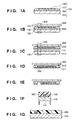
- a member 120 having a semiconductor film 110 with semiconductor elements and/or semiconductor integrated circuits 140 on a semiconductor region 130 via a separation layer 100 is prepared.
- a method of forming the semiconductor elements and/or semiconductor integrated circuits 140 on the semiconductor film 110 will be described later.
- the member 120 is separated at the separation layer 100. More specifically, a pressure by a fluid is applied to the side surface of the separation layer 100.
- a pressure preferably, a fluid formed from a liquid or gas is injected to the side surface of the separation layer 100 as high-pressure jet, or a static pressure is applied to the separation layer 100.
- the member 120 may be bonded to a support member 300 via an adhesive layer 310 (Fig. 1B).
- the step of bonding the member to the support member 300 may be omitted.
- the adhesive layer an epoxy-based adhesive or another adhesive can be used.
- the member 120 is separated at the separation layer 100 (Fig. 1C).
- the separation layer 100 is partitioned to desired semiconductor elements and/or semiconductor integrated circuits by kerfs to form chips (Fig. 1D), thereby obtaining one or a plurality of thin-film semiconductor devices 350. Then, cracks in the planar direction are formed in the separation layer 100 to separate the thin-film semiconductor devices 350 as chips from the member 120.
- the bottom surface of each kerf in Fig. 1D need not always reach the adhesive layer 310.
- the support member 300 is made of a stretchable material. In this case, even when the semiconductor film 110 is not completely separated, the chips can be extracted by stretching the support member 300.
- portions 111 of the separation layer 100 remain on the thin-film semiconductor devices 350.
- the remaining portions 111 may be removed by polishing, grinding, or etching. Instead polishing or the like, annealing in an atmosphere containing hydrogen may be executed.
- the remaining portions 111 on the bottom surfaces of the thin-film semiconductor devices 350 may be, e.g., individually removed.
- the thin-film semiconductor device 350 can be mounted on a support substrate 170 via the remaining separation layer 111, as shown in Fig. 1F, or can be transferred onto a plastic card, as shown in Fig. 1G.
- Reference numeral 180 denotes a sealing resin; 190, a wire; 200, a sealing resin/film; and 210, a plastic card. Since the remaining separation layer can serve as a gettering site, the resistance against metal contamination during the processes increases.
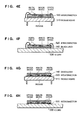
- Figs. 4A to 4H are enlarged views of a region 500 in Fig. 1B and regions related to it.
- Fig. 4A shows a state wherein the device layer 140 and support member 300 are bonded via the adhesive layer 310.
- Fig. 4B shows a state wherein separation was performed at the separation layer 100.
- Fig. 4C shows a state wherein the structure formed by bonding the support member 300 and device layer 140 is mounted on a package board 510.
- Reference numeral 515 denotes an adhesive layer.
- Fig. 4D shows a state wherein the semiconductor element and/or semiconductor integrated circuit 140 is separated from the support member 300.
- Fig. 4E shows a detailed example of a structure obtained by connecting the package board 510 and device layer by an interconnection 520.
- Fig. 4F shows an example in which the device is mounted on an IC card 530.
- an opposite side of the device layer 140 is bonded to the package board as a bonding surface.
- the device layer 140 side may be bonded to the package board as a bonding surface, as shown in Figs. 4G and 4H.
- a method using a porous layer formed by anodizing or a method using an ion-implanted layer formed by implanting ions of hydrogen, nitrogen, or a rare gas such as helium is mainly used.
- a silicon substrate is anodized to form the porous layer 100 functioning as a separation layer on the surface.
- the semiconductor film 110 is formed on the porous layer by CVD or the like, a semiconductor element and/or semiconductor integrated circuit is formed on the semiconductor film 110 by a normal semiconductor manufacturing process.
- the member 120 is obtained.
- a semiconductor element and/or semiconductor integrated circuit is formed on the surface of a silicon substrate (or epitaxial wafer).
- a protective film is formed on the surface of the element or the like as needed, hydrogen ions are implanted to a desired depth to form an ion-implanted layer functioning as a separation layer.
- the member 120 is obtained.
- a device may be formed in a region on the substrate surface side after the ion-implanted layer is formed at a predetermined depth from the silicon substrate surface. If the dose is large, a separation phenomenon may occur during the device forming process. Hence, the dose is reduced (and annealing is then performed as needed) for design not to cause separation during the device forming process.
- a plurality of porous layers having different porosities may be formed.
- a two-layered structure including a high-porosity layer and low-porosity layer from the semiconductor region 130 side may be formed.
- a three-layered structure including a first low-porosity layer, high-porosity layer, and second low-porosity layer from the semiconductor region 130 side may be formed.
- the porosity of a high-porosity layer can be 10% to 90%.
- the porosity of a low-porosity layer can be 0% to 70%.
- a protective film forming process of forming a protective film such as a nitride film or oxide film on the inner walls of pores in the porous layer or an annealing process in an atmosphere containing hydrogen is preferably performed before growing the semiconductor film 110 on the porous layer. It is also preferable to execute the annealing process after the protective film forming process.
- the semiconductor film 110 is preferably slowly grown at 20 nm/min or less to a predetermined thickness (e.g., 10 nm).
- a non-porous single-crystal silicon thin film or a compound semiconductor film such as a GaAs, InP, or GaN film can be used.
- the semiconductor film is made of single-crystal silicon, SiH 2 Cl 2 , SiHCl 3 , SiCl 4 , SiH 4 , or HCl gas may be added as a source gas.
- the forming method is not limited to CVD, and MBE or sputtering can also be used.
- second annealing is preferably executed at a temperature higher than that for the first annealing before the thin film is grown.
- the first annealing temperature can be 800°C to 1,000°C
- the second annealing temperature can be 900°C to melting point.
- pores on the surface of the porous layer can be sufficiently sealed.
- the first annealing may be executed at 950°C
- the second annealing may be executed at 1,100°C.
- the member 120 not only a single-crystal silicon wafer prepared by the CZ method, MCZ method, or FZ method but also a wafer having a substrate surface annealed in hydrogen or epitaxial silicon wafer can also be used. Not only silicon but also a compound semiconductor substrate such as a GaAs substrate or InP substrate can be used.
- an element such as a CMOS, bipolar transistor, diode, coil, or capacitor, or a semiconductor integrated circuit such as a DRAM, microprocessor, logic IC, or memory can be formed.
- the application purposes of the element or circuit include an electronic circuit, oscillation circuit, light receiving/emitting element, optical waveguide, and various sensors.
- a trench or LOCOS (local oxidation) portion used for element isolation is also preferably made to reach the porous layer.
- Portions between the prospective separated chips may be subjected to LOCOS or mesa etching to remove the semiconductor film between the chips.
- a fluid such as a liquid or gas, i.e., high-pressure fluid jet is injected to the side surface of the separation layer.
- a liquid such as water, an etchant, or alcohol, or a gas such as air, nitrogen gas, or argon gas can be used.
- An ultrasonic vibration may be applied in separation.
- the porous layer or ion-implanted layer serving as a separation layer may be exposed.
- a closed space forming member for forming a closed space by surrounding at least part of the peripheral portion of the member, and a pressure application mechanism capable of applying a pressure higher than that of the external space into the closed space are required.
- a microcavity layer formed by ion implantation coagulates.
- a chip may be separated using this phenomenon in addition to a pressure by a fluid.
- the structure may be heated by a CO 2 laser or the like.
- a normal dicing apparatus can be used.
- etching laser abrasion, ultrasonic cutter, or high-pressure jet (e.g., water jet) can be used.
- high-pressure jet e.g., water jet
- etching HF + H 2 O 2 , HF + HNO 3 , or an alkali solution can be used as an etchant.
- the laser are a YAG laser, CO 2 laser, and excimer laser.
- a member 120 having a semiconductor film 110 with semiconductor elements and/or semiconductor integrated circuits 140 on a semiconductor region 130 via a separation layer 100 is prepared. (Fig. 2A).
- the member 120 is bonded to a support member 300 via an adhesive layer 310, as needed (Fig. 2B).
- kerfs 400 are formed in the member 120 from the semiconductor region 130 side to separate the member into desired semiconductor elements and/or semiconductor integrated circuits, thereby forming chips (Fig. 2B).
- the bottom surface of each kerf preferably reaches a portion near the interface between the semiconductor film 110 and the support member 300 or a portion near the adhesive layer 310.
- a small semiconductor region 500 formed as a chip is separated from the member 120 (Fig. 2C).
- a thin-film semiconductor device is manufactured.
- Figs. 2D to 2F show an example of a method of packaging the thin-film semiconductor device 500.
- the small semiconductor region 500 is mounted on a plastic card. After the small semiconductor region 500 is separated at a separation layer 115, the resultant structure is sealed by a resin 200.
- the packaging method is not limited to this.
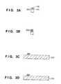
- the small semiconductor region 500 may be extracted, as shown in Fig. 3A, separated by forming a crack in the planar direction in the separation layer 115 (Fig. 3B), and mounted on a substrate 215.
- the semiconductor element side may face upward, as shown in Fig. 3C, or may be used as a bonding surface, as shown in Fig. 3D.
- the separation step is executed after a chip is formed, i.e., after the separation area is largely decreased as compared to the entire silicon wafer.
- an external force such as a tensile force, compression force, or shearing force may be used.
- the region is separated using the above-described fluid.
- the region may be separated by heating the separation layer 115.
- the separation layer is also preferably locally heated using a laser or the like.
- the separation step is executed after the chip forming step, as in this embodiment, local stress concentration to a semiconductor element can be reduced as compared to a case wherein a large-area portion is separated at once. Additionally, when only non-defective chips are separated, the yield can be improved.
- a p-type single-crystal Si substrate having a resistivity of 0.01 ⁇ cm was prepared.
- the substrate surface was anodized in an HF solution.
- the anodizing conditions were
- the porosity of the porous Si layer was adjusted such that a high-quality epitaxial Si layer could be formed on the porous Si layer and the porous Si layer could be used as a separation layer. More specifically, the porosity was 20%.
- the thickness of the porous Si layer is not limited to the above thickness and may be several hundred ⁇ m to 0.1 ⁇ m.
- the type of the single-crystal Si substrate is not limited to the p type and may be n type.
- the resistivity of the substrate is not limited to the particular value.
- the substrate typically has a resistivity ranges from 0.001 to 50 ⁇ ⁇ cm, preferably from 0.005 to 1 ⁇ ⁇ cm, and more preferably from 0.005 to 0.1 ⁇ ⁇ cm.
- This single-crystal Si substrate was oxidized in an oxygen atmosphere at 400°C for 1 hr.
- the inner walls of pores in the porous Si layer were covered with a thermal oxide film.
- the surface of the porous Si layer was dipped in hydrofluoric acid to remove only the oxide film on the surface of the porous Si layer while leaving the oxide film on the inner walls of the pores.
- a 3- ⁇ m thick single-crystal Si layer was epitaxially grown on the porous Si layer by CVD (Chemical Vapor Deposition). The growth conditions were
- the single-crystal Si layer may be grown on the porous Si layer to have a thickness ranges from several nm to several hundred ⁇ m in accordance with applications or devices to be manufactured.
- annealing was executed in an atmosphere containing hydrogen. The purpose was to seal surface pores.
- small Si atoms may be added by a source gas or the like to compensate for atoms for surface pore sealing.
- a resultant member can be handled as a wafer that is identical to a normal epitaxial wafer. Only a different point is that the porous Si layer is formed under the epitaxial layer. A circuit such as a microprocessor, logic IC, or memory was formed on the epitaxial layer. With the same processes as in normal manufacturing, an LSI having performance identical to a conventional LSI could be formed. After epitaxial growth and before device region formation, it is also preferable to anneal the structure in a hydrogen atmosphere.
- a Si region of the porous Si layer is depleted and has a high resistance.
- Example 1 The thus formed LSI is normally subjected to lower-surface grinding and chip formation by dicing.
- Example 1 the entire wafer was separated into the substrate side and LSI side at a porous Si layer formed in advance.
- a fluid pressure was used. More specifically, separation was performed by injecting high-pressure water jet to the side surface of the porous Si layer.
- a gas, a liquid, or a gas or liquid containing solid granules or powder can preferably be used.
- water jet to be referred to as "WJ" hereinafter
- air jet, nitrogen gas jet or another gas jet, liquid jet except water, liquid jet containing ice or plastic pieces or abrasives, or a static pressure thereof may be applied.
- a characteristic feature of a fluid it can enter a very small gap to increase the internal pressure and also distribute the external pressure.
- a portion that is most readily separated can be selectively separated. This is an optimum means for separating the entire thin layer on which semiconductor devices have already been formed, as in the present invention.
- the surface side is preferably supported by another support member.
- a flexible sheet, glass substrate, plastic substrate, metal substrate, or another semiconductor substrate can be used.
- Such a support member is bonded to the device formation surface side of the substrate with an adhesive.
- a fluid was applied to a portion near the edge of the first substrate supported by the support member to separate the entire porous Si layer.
- the porous Si layer is preferably exposed to the edge of the first substrate.
- a fluid pressure can be more efficiently applied to the porous Si layer.
- the porous Si remaining on the device layer side may be removed or not.
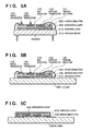
- FIG. 5A shows a schematic view.
- Reference numeral 510 denotes a package board; 520, an interconnection; 141, trench isolation; 142, a bipolar transistor; 143, well isolation; 144, a PMOS transistor; 145, an NMOS transistor.
- the trench isolation 141 may reach a separation layer 100.
- an IC card When a semiconductor device is directly mounted on a plastic card, an IC card can be formed.
- Fig. 5B shows an example in which the device is mounted on an IC card while making the device layer side face upward.
- Fig. 5C shows an example in which the device layer side faces downward.
- the heat dissipation properties can be greatly improved as compared to a conventional back grinder scheme.
- the thickness of the wafer that can be achieved by back-grinding the back surface of the wafer using the back grinder is to a several hundred ⁇ m.
- the "thickness of surface epitaxial layer + thickness of part of porous Si layer (total thickness ⁇ 10 ⁇ m)" is to be formed on the epitaxial layer, and the chip may be packaged on a transparent substrate or optical waveguide.
- the chip size is preferably 10 cm ⁇ 10 cm or less, more preferably, 5 cm ⁇ 5 cm or less, and most preferably 2 cm ⁇ 2 cm or less.
- the single-crystal Si substrate that remained after separation could be re-used in the same process after surface re-polishing, etching, or annealing in an atmosphere containing hydrogen was executed as needed.
- the substrate may be used for another purpose.
- Example 1 a single porous layer was used. In Example 2, two porous layers having different porosities were formed.
- a high-porosity layer having a porosity of 45% and a low-porosity layer having a porosity of 20% were formed from the single-crystal silicon substrate side.
- an epitaxial silicon layer was formed on the low-porosity layer under the same conditions as in Example 1, and an integrated circuit and the like were formed.
- the thicknesses of the two porous layers need not always be 6 ⁇ m/3 ⁇ m.
- the thicknesses can be changed by changing the anodizing conditions.
- another alcohol such as IPA (isopropyl alcohol) may be used.
- An alcohol serving as a surfactant aims at preventing reactive bubbles from sticking to a wafer surface.
- a surfactant other than an alcohol may be used.
- surface sticking bubbles may be removed by an ultrasonic wave without adding any surfactant.
- Example 2 After separation, the same chip forming step as in Example 1 was performed to manufacture a thin-film semiconductor device.
- a p-type single-crystal Si substrate having a resistivity of 14 ⁇ cm was prepared.
- the plane orientation was ⁇ 100>.
- a circuit formation layer for a microprocessor, logic IC, memory, or the like was formed on the surface of the single-crystal Si substrate.
- Hydrogen ions were implanted from the circuit formation layer side to a predetermined depth (in Example 3, a depth of 0.5 ⁇ m from the surface side), thereby forming an ion-implanted layer.
- the dose was several 10 16 to 10 17 /cm 2 .
- a protective film of SiO 2 may be formed on the uppermost surface by CVD.
- the device formation layer and a plastic substrate (or a glass substrate, Si substrate, flexible film, or adhesive tape) serving as a support member were bonded with an adhesive.
- nitrogen ions were injected to the side surface of the ion-implanted layer to execute the separation step.
- the chip forming step was performed, as in Example 1, to form an IC card.
- a p-type single-crystal Si substrate having a resistivity of 0.01 ⁇ cm was prepared.
- the substrate surface was anodized in an HF solution.
- the anodizing conditions were
- a high-porosity layer having a porosity of 45% and a low-porosity layer having a porosity of 20% were formed from the single-crystal silicon substrate side.
- an epitaxial silicon layer was formed on the low-porosity layer under the same conditions as in Example 1, and an integrated circuit and the like were formed.
- the device layer side was bonded to a plastic substrate (or a glass substrate, Si substrate, flexible film, or adhesive tape) serving as a support member with an adhesive.
- dicing, i.e., chip formation was performed from an opposite side of the epitaxial layer, i.e., the single-crystal silicon substrate side, thereby separating the substrate into small regions.
- the above-described adhesive was, e.g., melted, as needed, to extract a chip.
- the chip was mounted on a package board such that the device layer side was used as a bonding surface. After that, a tensile force was applied to separate the substrate at the separation layer. In this way, a thin-film semiconductor device could be formed on the package board.
- This chip was sealed with a plastic resin to form an IC card.
- the separation step in forming a thin-film semiconductor device is executed using a fluid or executed after a silicon wafer is formed into desired small regions. With this process, a thin-film semiconductor device can be manufactured with a reduced influence on the device formation layer in separation.
- a thin-film semiconductor device with a reduced influence on a device formation layer in separation and a method of manufacturing the device are provided.
- the manufacturing method includes the step of preparing a member having a semiconductor film with a semiconductor element and/or semiconductor integrated circuit on a separation layer, the separation step of separating the member at the separation layer by a pressure of a fluid, and the chip forming step of, after the separation step, forming the semiconductor film into chips.
Landscapes
- Dicing (AREA)
- Recrystallisation Techniques (AREA)
- Thin Film Transistor (AREA)
Abstract


Description
Claims (12)
- A method of manufacturing a thin-film semiconductor device, comprising:the step of preparing a member having a semiconductor film with a semiconductor element and/or semiconductor integrated circuit on a separation layer;the separation step of separating the member at the separation layer by a pressure of a fluid; andthe chip forming step of, after the separation step, forming the semiconductor film into chips.
- The method according to claim 1, wherein the member is obtained by forming a porous layer on a surface of a semiconductor substrate, forming the semiconductor film on a surface of the porous layer, and then forming the semiconductor element and/or semiconductor integrated circuit.
- The method according to claim 2, wherein the semiconductor film is formed on the surface of the porous layer after forming a protective film on inner walls of pores in the porous layer.
- The method according to claim 1, wherein the member is obtained by forming the semiconductor element and/or semiconductor integrated circuit on a surface of a semiconductor substrate and implanting ions from the surface side to a predetermined depth to form the separation layer.
- The method according to claim 2, wherein the semiconductor substrate is a single-crystal silicon substrate or a compound semiconductor substrate.
- The method according to claim 4, wherein the semiconductor substrate is a single-crystal silicon substrate or a compound semiconductor substrate.
- The method according to claim 1, wherein the separation step is executed by applying the pressure of the fluid to the separation layer.
- The method according to claim 1, wherein after the separation step, the separation layer remaining on the semiconductor film side is removed, and then, the chip forming step is executed.
- The method according to claim 1, wherein after the separation step and the chip forming step, the step of removing the separation layer remaining on the semiconductor film side is executed.
- A method of manufacturing a thin-film semiconductor device, comprising:the step of preparing a member having a semiconductor film with a semiconductor element and/or semiconductor integrated circuit on a separation layer;the chip forming step of forming the member into chips in desired regions; andthe separation step of, after the chip forming step, separating the member at the separation layer.
- A thin-film semiconductor device obtaining by processing a member having a semiconductor film with a semiconductor element and/or semiconductor integrated circuit on a separation layer, the process comprising:the separation step of separating the member at the separation layer by a pressure of a fluid; andthe chip forming step of, after the separation step, forming the semiconductor film into chips.
- A thin-film semiconductor device obtaining by processing a member having a semiconductor film with a semiconductor element and/or semiconductor integrated circuit on a separation layer, the process comprising:the chip forming step of forming the member into chips in desired regions; andthe separation step of, after the chip forming step, separating the member at the separation layer.
Applications Claiming Priority (2)
| Application Number | Priority Date | Filing Date | Title |
|---|---|---|---|
| JP2001023847 | 2001-01-31 | ||
| JP2001023847A JP4803884B2 (en) | 2001-01-31 | 2001-01-31 | Method for manufacturing thin film semiconductor device |
Publications (2)
| Publication Number | Publication Date |
|---|---|
| EP1229582A2 true EP1229582A2 (en) | 2002-08-07 |
| EP1229582A3 EP1229582A3 (en) | 2005-10-19 |
Family
ID=18889079
Family Applications (1)
| Application Number | Title | Priority Date | Filing Date |
|---|---|---|---|
| EP02002259A Withdrawn EP1229582A3 (en) | 2001-01-31 | 2002-01-30 | Thin-film semiconductor device and method of manufacturing the same |
Country Status (3)
| Country | Link |
|---|---|
| US (2) | US20020100941A1 (en) |
| EP (1) | EP1229582A3 (en) |
| JP (1) | JP4803884B2 (en) |
Cited By (9)
| Publication number | Priority date | Publication date | Assignee | Title |
|---|---|---|---|---|
| EP1434262A3 (en) * | 2002-12-26 | 2006-09-20 | Semiconductor Energy Laboratory Co., Ltd. | Semiconductor device manufactured by the transfer technique |
| US7436050B2 (en) | 2003-01-22 | 2008-10-14 | Semiconductor Energy Laboratory Co., Ltd. | Semiconductor device having a flexible printed circuit |
| US7576362B2 (en) | 2003-03-14 | 2009-08-18 | Semiconductor Energy Laboratory Co., Ltd. | Semiconductor device having EL element, integrated circuit and adhesive layer therebetween |
| US7709337B2 (en) | 2007-04-20 | 2010-05-04 | Semiconductor Energy Laboratory Co., Ltd. | Method for manufacturing SOI substrate and semiconductor device |
| US7755085B2 (en) | 2005-05-13 | 2010-07-13 | Sharp Kabushiki Kaisha | Semiconductor device and method for fabricating same |
| WO2010116662A1 (en) * | 2009-04-06 | 2010-10-14 | Canon Kabushiki Kaisha | Semiconductor device and method for manufacturing semiconductor device |
| US8030745B2 (en) | 2004-03-04 | 2011-10-04 | Semiconductor Energy Laboratory Co., Ltd. | ID chip and IC card |
| US8211780B2 (en) | 2007-12-03 | 2012-07-03 | Semiconductor Energy Laboratory Co., Ltd. | Method for manufacturing SOI substrate |
| WO2018190950A3 (en) * | 2017-04-14 | 2018-11-15 | Qualcomm Incorporated | Porous silicon dicing |
Families Citing this family (97)
| Publication number | Priority date | Publication date | Assignee | Title |
|---|---|---|---|---|
| JP4708577B2 (en) | 2001-01-31 | 2011-06-22 | キヤノン株式会社 | Method for manufacturing thin film semiconductor device |
| JP4803884B2 (en) * | 2001-01-31 | 2011-10-26 | キヤノン株式会社 | Method for manufacturing thin film semiconductor device |
| JP2002229473A (en) | 2001-01-31 | 2002-08-14 | Canon Inc | Display device manufacturing method |
| JP2003258210A (en) | 2001-12-27 | 2003-09-12 | Canon Inc | Display device and method of manufacturing the same |
| US7119365B2 (en) | 2002-03-26 | 2006-10-10 | Sharp Kabushiki Kaisha | Semiconductor device and manufacturing method thereof, SOI substrate and display device using the same, and manufacturing method of the SOI substrate |
| US6682955B2 (en) * | 2002-05-08 | 2004-01-27 | Micron Technology, Inc. | Stacked die module and techniques for forming a stacked die module |
| US6907176B2 (en) * | 2002-06-24 | 2005-06-14 | Dow Corning Corporation | Planar optical waveguide assembly and method of preparing same |
| US7508034B2 (en) * | 2002-09-25 | 2009-03-24 | Sharp Kabushiki Kaisha | Single-crystal silicon substrate, SOI substrate, semiconductor device, display device, and manufacturing method of semiconductor device |
| JP4837240B2 (en) * | 2002-09-25 | 2011-12-14 | シャープ株式会社 | Semiconductor device |
| US7056810B2 (en) * | 2002-12-18 | 2006-06-06 | Semiconductor Energy Laboratory Co., Ltd. | Method for manufacturing semiconductor apparatus, and semiconductor apparatus and electric appliance |
| US6759277B1 (en) * | 2003-02-27 | 2004-07-06 | Sharp Laboratories Of America, Inc. | Crystalline silicon die array and method for assembling crystalline silicon sheets onto substrates |
| JP2004288834A (en) * | 2003-03-20 | 2004-10-14 | Fujitsu Ltd | Electronic component mounting method, mounting structure and package substrate |
| JP2004335642A (en) * | 2003-05-06 | 2004-11-25 | Canon Inc | Substrate and manufacturing method thereof |
| KR20060017771A (en) * | 2003-05-06 | 2006-02-27 | 캐논 가부시끼가이샤 | Semiconductor substrate, semiconductor device, light emitting diode and manufacturing method |
| US20050124137A1 (en) * | 2003-05-07 | 2005-06-09 | Canon Kabushiki Kaisha | Semiconductor substrate and manufacturing method therefor |
| TWI242232B (en) * | 2003-06-09 | 2005-10-21 | Canon Kk | Semiconductor substrate, semiconductor device, and method of manufacturing the same |
| JP2005005509A (en) * | 2003-06-12 | 2005-01-06 | Canon Inc | Thin film transistor and manufacturing method thereof |
| JP2005026472A (en) * | 2003-07-02 | 2005-01-27 | Sharp Corp | Manufacturing method of semiconductor device |
| JP2005136214A (en) * | 2003-10-30 | 2005-05-26 | Nec Corp | Method for manufacturing thin film device substrate |
| US20050132332A1 (en) * | 2003-12-12 | 2005-06-16 | Abhay Sathe | Multi-location coordinated test apparatus |
| JP2006012914A (en) | 2004-06-22 | 2006-01-12 | Canon Inc | Integrated circuit chip manufacturing method and semiconductor device |
| JP4771510B2 (en) * | 2004-06-23 | 2011-09-14 | キヤノン株式会社 | Semiconductor layer manufacturing method and substrate manufacturing method |
| WO2006012544A2 (en) * | 2004-07-22 | 2006-02-02 | The Board Of Trustees Of The Leland Stanford Junior University | Germanium substrate-type materials and approach therefor |
| JP4759948B2 (en) * | 2004-07-28 | 2011-08-31 | ルネサスエレクトロニクス株式会社 | Manufacturing method of semiconductor device |
| JP4838504B2 (en) | 2004-09-08 | 2011-12-14 | キヤノン株式会社 | Manufacturing method of semiconductor device |
| US8137417B2 (en) | 2006-09-29 | 2012-03-20 | Semiconductor Energy Laboratory Co., Ltd. | Peeling apparatus and manufacturing apparatus of semiconductor device |
| TWI430435B (en) | 2006-09-29 | 2014-03-11 | 半導體能源研究所股份有限公司 | Semiconductor device manufacturing method |
| JP5171016B2 (en) * | 2006-10-27 | 2013-03-27 | キヤノン株式会社 | Semiconductor member, manufacturing method of semiconductor article, and LED array using the manufacturing method |
| HK1109708A2 (en) * | 2007-04-24 | 2008-06-13 | On Track Innovations Ltd. | Interface card and apparatus and process for the formation thereof |
| JP5498670B2 (en) * | 2007-07-13 | 2014-05-21 | 株式会社半導体エネルギー研究所 | Method for manufacturing semiconductor substrate |
| JP5367330B2 (en) * | 2007-09-14 | 2013-12-11 | 株式会社半導体エネルギー研究所 | Method for manufacturing SOI substrate and method for manufacturing semiconductor device |
| JP2009094144A (en) * | 2007-10-04 | 2009-04-30 | Canon Inc | Method for manufacturing light emitting device |
| US8236668B2 (en) * | 2007-10-10 | 2012-08-07 | Semiconductor Energy Laboratory Co., Ltd. | Method for manufacturing SOI substrate |
| US20090123743A1 (en) * | 2007-11-14 | 2009-05-14 | Guy Shafran | Method of manufacture of wire imbedded inlay |
| US8028923B2 (en) * | 2007-11-14 | 2011-10-04 | Smartrac Ip B.V. | Electronic inlay structure and method of manufacture thereof |
| US20100244136A1 (en) * | 2007-12-27 | 2010-09-30 | Sharp Kabushiki Kaisha | Semiconductor device, single-crystal semiconductor thin film-including substrate, and production methods thereof |
| KR100937721B1 (en) | 2008-03-28 | 2010-01-20 | 앰코 테크놀로지 코리아 주식회사 | Method of manufacturing semiconductor package using PSS |
| US20090311849A1 (en) * | 2008-06-17 | 2009-12-17 | International Business Machines Corporation | Methods of separating integrated circuit chips fabricated on a wafer |
| FR2936357B1 (en) * | 2008-09-24 | 2010-12-10 | Commissariat Energie Atomique | METHOD FOR DEFLECTING CHIPS ON A SUBSTRATE |
| US20100090008A1 (en) * | 2008-10-13 | 2010-04-15 | Oded Bashan | Authentication seal |
| JP5586920B2 (en) * | 2008-11-20 | 2014-09-10 | 株式会社半導体エネルギー研究所 | Method for manufacturing flexible semiconductor device |
| US8507966B2 (en) | 2010-03-02 | 2013-08-13 | Micron Technology, Inc. | Semiconductor cells, arrays, devices and systems having a buried conductive line and methods for forming the same |
| US9161448B2 (en) | 2010-03-29 | 2015-10-13 | Semprius, Inc. | Laser assisted transfer welding process |
| US8546237B2 (en) * | 2010-08-31 | 2013-10-01 | Oepic Semiconductors, Inc. | Transferring and resizing of epitaxial film arrays and method thereof |
| US8997832B1 (en) | 2010-11-23 | 2015-04-07 | Western Digital (Fremont), Llc | Method of fabricating micrometer scale components |
| US9899329B2 (en) | 2010-11-23 | 2018-02-20 | X-Celeprint Limited | Interconnection structures and methods for transfer-printed integrated circuit elements with improved interconnection alignment tolerance |
| US9391220B2 (en) * | 2011-02-07 | 2016-07-12 | The Trustees Of Princeton University | System and method for interfacing large-area electronics with integrated circuit devices |
| JP5839538B2 (en) * | 2011-03-17 | 2016-01-06 | リンテック株式会社 | Manufacturing method of thin semiconductor device |
| US9781783B2 (en) | 2011-04-15 | 2017-10-03 | Semiconductor Energy Laboratory Co., Ltd. | Light-emitting device, display device, light-emitting system, and display system |
| US8934259B2 (en) | 2011-06-08 | 2015-01-13 | Semprius, Inc. | Substrates with transferable chiplets |
| KR101819133B1 (en) * | 2011-06-30 | 2018-01-16 | 삼성전자주식회사 | Methods of forming semiconductor modules and semiconductor modules formed of the same |
| US9412727B2 (en) | 2011-09-20 | 2016-08-09 | Semprius, Inc. | Printing transferable components using microstructured elastomeric surfaces with pressure modulated reversible adhesion |
| CN105474355B (en) | 2013-08-06 | 2018-11-13 | 株式会社半导体能源研究所 | Stripping method |
| TWI777433B (en) | 2013-09-06 | 2022-09-11 | 日商半導體能源研究所股份有限公司 | Light-emitting device and method for manufacturing light-emitting device |
| US9937698B2 (en) | 2013-11-06 | 2018-04-10 | Semiconductor Energy Laboratory Co., Ltd. | Peeling method and light-emitting device |
| TWI814461B (en) | 2014-06-18 | 2023-09-01 | 愛爾蘭商艾克斯展示公司技術有限公司 | Micro assembled led displays and lighting elements |
| TWI659475B (en) | 2014-07-20 | 2019-05-11 | 愛爾蘭商艾克斯瑟樂普林特有限公司 | Device and method for micro-repost printing |
| TWI695525B (en) | 2014-07-25 | 2020-06-01 | 日商半導體能源研究所股份有限公司 | Separation method, light-emitting device, module, and electronic device |
| US9991163B2 (en) | 2014-09-25 | 2018-06-05 | X-Celeprint Limited | Small-aperture-ratio display with electrical component |
| US9799719B2 (en) | 2014-09-25 | 2017-10-24 | X-Celeprint Limited | Active-matrix touchscreen |
| US9871345B2 (en) | 2015-06-09 | 2018-01-16 | X-Celeprint Limited | Crystalline color-conversion device |
| US10133426B2 (en) | 2015-06-18 | 2018-11-20 | X-Celeprint Limited | Display with micro-LED front light |
| US11061276B2 (en) | 2015-06-18 | 2021-07-13 | X Display Company Technology Limited | Laser array display |
| US9704821B2 (en) | 2015-08-11 | 2017-07-11 | X-Celeprint Limited | Stamp with structured posts |
| US10468363B2 (en) | 2015-08-10 | 2019-11-05 | X-Celeprint Limited | Chiplets with connection posts |
| US10380930B2 (en) | 2015-08-24 | 2019-08-13 | X-Celeprint Limited | Heterogeneous light emitter display system |
| US10230048B2 (en) | 2015-09-29 | 2019-03-12 | X-Celeprint Limited | OLEDs for micro transfer printing |
| US10066819B2 (en) | 2015-12-09 | 2018-09-04 | X-Celeprint Limited | Micro-light-emitting diode backlight system |
| US9786646B2 (en) | 2015-12-23 | 2017-10-10 | X-Celeprint Limited | Matrix addressed device repair |
| US10259207B2 (en) | 2016-01-26 | 2019-04-16 | Semiconductor Energy Laboratory Co., Ltd. | Method for forming separation starting point and separation method |
| TWI710061B (en) | 2016-02-25 | 2020-11-11 | 愛爾蘭商艾克斯展示公司技術有限公司 | Efficiently micro-transfer printing micro-scale devices onto large-format substrates |
| US10193025B2 (en) | 2016-02-29 | 2019-01-29 | X-Celeprint Limited | Inorganic LED pixel structure |
| US10153257B2 (en) | 2016-03-03 | 2018-12-11 | X-Celeprint Limited | Micro-printed display |
| US10153256B2 (en) | 2016-03-03 | 2018-12-11 | X-Celeprint Limited | Micro-transfer printable electronic component |
| US10103069B2 (en) | 2016-04-01 | 2018-10-16 | X-Celeprint Limited | Pressure-activated electrical interconnection by micro-transfer printing |
| US10008483B2 (en) | 2016-04-05 | 2018-06-26 | X-Celeprint Limited | Micro-transfer printed LED and color filter structure |
| US10199546B2 (en) | 2016-04-05 | 2019-02-05 | X-Celeprint Limited | Color-filter device |
| US9997501B2 (en) | 2016-06-01 | 2018-06-12 | X-Celeprint Limited | Micro-transfer-printed light-emitting diode device |
| US11137641B2 (en) | 2016-06-10 | 2021-10-05 | X Display Company Technology Limited | LED structure with polarized light emission |
| US10222698B2 (en) | 2016-07-28 | 2019-03-05 | X-Celeprint Limited | Chiplets with wicking posts |
| US11064609B2 (en) | 2016-08-04 | 2021-07-13 | X Display Company Technology Limited | Printable 3D electronic structure |
| US9980341B2 (en) | 2016-09-22 | 2018-05-22 | X-Celeprint Limited | Multi-LED components |
| US10782002B2 (en) | 2016-10-28 | 2020-09-22 | X Display Company Technology Limited | LED optical components |
| US10347168B2 (en) | 2016-11-10 | 2019-07-09 | X-Celeprint Limited | Spatially dithered high-resolution |
| EP3542394B1 (en) | 2016-11-15 | 2025-09-24 | X Display Company Technology Limited | Micro-transfer-printable flip-chip structures and manufacturing methods thereof |
| US10600671B2 (en) | 2016-11-15 | 2020-03-24 | X-Celeprint Limited | Micro-transfer-printable flip-chip structures and methods |
| US10395966B2 (en) | 2016-11-15 | 2019-08-27 | X-Celeprint Limited | Micro-transfer-printable flip-chip structures and methods |
| US10438859B2 (en) | 2016-12-19 | 2019-10-08 | X-Celeprint Limited | Transfer printed device repair |
| US10396137B2 (en) | 2017-03-10 | 2019-08-27 | X-Celeprint Limited | Testing transfer-print micro-devices on wafer |
| US11024608B2 (en) | 2017-03-28 | 2021-06-01 | X Display Company Technology Limited | Structures and methods for electrical connection of micro-devices and substrates |
| WO2019018328A1 (en) * | 2017-07-17 | 2019-01-24 | Cornell University | Sonic testing method, apparatus and applications |
| JP6991673B2 (en) | 2018-02-27 | 2022-01-12 | 株式会社ディスコ | Peeling method |
| US10796971B2 (en) | 2018-08-13 | 2020-10-06 | X Display Company Technology Limited | Pressure-activated electrical interconnection with additive repair |
| CN111463172A (en) * | 2019-01-21 | 2020-07-28 | 瀚宇彩晶股份有限公司 | Manufacturing method of electronic device |
| US10748793B1 (en) | 2019-02-13 | 2020-08-18 | X Display Company Technology Limited | Printing component arrays with different orientations |
| WO2021015816A1 (en) * | 2019-07-19 | 2021-01-28 | Iqe Plc | Semiconductor material having tunable permittivity and tunable thermal conductivity |
| GB2612040B (en) | 2021-10-19 | 2025-02-12 | Iqe Plc | Porous distributed Bragg reflector apparatuses, systems, and methods |
Family Cites Families (57)
| Publication number | Priority date | Publication date | Assignee | Title |
|---|---|---|---|---|
| US100941A (en) * | 1870-03-15 | Improvement in corn-huskers | ||
| US622513A (en) * | 1899-04-04 | Apparatus for manufacturing mirrors | ||
| US76904A (en) * | 1868-04-21 | James e | ||
| JPS55145354A (en) | 1979-04-27 | 1980-11-12 | Nec Home Electronics Ltd | Separating method of semiconductor pellet |
| US5158818A (en) * | 1984-01-30 | 1992-10-27 | National Starch And Chemical Investment Holding Corporation | Conductive die attach tape |
| US5071792A (en) * | 1990-11-05 | 1991-12-10 | Harris Corporation | Process for forming extremely thin integrated circuit dice |
| US5206749A (en) * | 1990-12-31 | 1993-04-27 | Kopin Corporation | Liquid crystal display having essentially single crystal transistors pixels and driving circuits |
| US5256562A (en) * | 1990-12-31 | 1993-10-26 | Kopin Corporation | Method for manufacturing a semiconductor device using a circuit transfer film |
| WO1993021663A1 (en) | 1992-04-08 | 1993-10-28 | Georgia Tech Research Corporation | Process for lift-off of thin film materials from a growth substrate |
| EP0603973A3 (en) | 1992-12-23 | 1995-06-28 | Philips Electronics Nv | Semiconductor component having p-n junctions separated by trenches and its manufacturing process. |
| DE4317721C1 (en) * | 1993-05-27 | 1994-07-21 | Siemens Ag | Process for separating chips from a wafer |
| JP3257580B2 (en) * | 1994-03-10 | 2002-02-18 | キヤノン株式会社 | Manufacturing method of semiconductor substrate |
| US5942768A (en) * | 1994-10-07 | 1999-08-24 | Semionductor Energy Laboratory Co., Ltd. | Semiconductor device having improved crystal orientation |
| JP3381443B2 (en) * | 1995-02-02 | 2003-02-24 | ソニー株式会社 | Method for separating semiconductor layer from substrate, method for manufacturing semiconductor device, and method for manufacturing SOI substrate |
| US6107213A (en) * | 1996-02-01 | 2000-08-22 | Sony Corporation | Method for making thin film semiconductor |
| US5757456A (en) * | 1995-03-10 | 1998-05-26 | Semiconductor Energy Laboratory Co., Ltd. | Display device and method of fabricating involving peeling circuits from one substrate and mounting on other |
| CN1132223C (en) * | 1995-10-06 | 2003-12-24 | 佳能株式会社 | Semiconductor substrate and producing method thereof |
| JP3893645B2 (en) * | 1996-03-18 | 2007-03-14 | ソニー株式会社 | Thin film semiconductor device and IC card manufacturing method |
| DE19613561C2 (en) * | 1996-04-04 | 2002-04-11 | Micronas Gmbh | Method for separating electrically tested electronic elements connected to one another in a body |
| KR100481994B1 (en) | 1996-08-27 | 2005-12-01 | 세이코 엡슨 가부시키가이샤 | Stripping method, transfer method of thin film device, and thin film device, thin film integrated circuit device and liquid crystal display device manufactured using the same |
| WO1998013862A1 (en) * | 1996-09-24 | 1998-04-02 | Mitsubishi Denki Kabushiki Kaisha | Semiconductor device and production method thereof |
| JP3948035B2 (en) * | 1996-10-18 | 2007-07-25 | ソニー株式会社 | Method for creating bonded SOI substrate |
| EP0849788B1 (en) | 1996-12-18 | 2004-03-10 | Canon Kabushiki Kaisha | Process for producing semiconductor article by making use of a substrate having a porous semiconductor layer |
| EP0851513B1 (en) * | 1996-12-27 | 2007-11-21 | Canon Kabushiki Kaisha | Method of producing semiconductor member and method of producing solar cell |
| SG68035A1 (en) * | 1997-03-27 | 1999-10-19 | Canon Kk | Method and apparatus for separating composite member using fluid |
| JP3492142B2 (en) * | 1997-03-27 | 2004-02-03 | キヤノン株式会社 | Manufacturing method of semiconductor substrate |
| US6159824A (en) * | 1997-05-12 | 2000-12-12 | Silicon Genesis Corporation | Silicon-on-silicon wafer bonding process using a thin film blister-separation method |
| AU7685198A (en) * | 1997-05-12 | 1998-12-08 | Silicon Genesis Corporation | A controlled cleavage process |
| JPH115064A (en) | 1997-06-16 | 1999-01-12 | Canon Inc | Sample separation apparatus and method, and substrate manufacturing method |
| JP3738798B2 (en) * | 1997-07-03 | 2006-01-25 | セイコーエプソン株式会社 | Method for manufacturing active matrix substrate and method for manufacturing liquid crystal panel |
| US6306729B1 (en) * | 1997-12-26 | 2001-10-23 | Canon Kabushiki Kaisha | Semiconductor article and method of manufacturing the same |
| US6075280A (en) * | 1997-12-31 | 2000-06-13 | Winbond Electronics Corporation | Precision breaking of semiconductor wafer into chips by applying an etch process |
| US6017804A (en) * | 1998-01-09 | 2000-01-25 | Lucent Technologies Inc. | Method and apparatus for cleaving semiconductor material |
| MY118019A (en) * | 1998-02-18 | 2004-08-30 | Canon Kk | Composite member, its separation method, and preparation method of semiconductor substrate by utilization thereof |
| JP3031904B2 (en) | 1998-02-18 | 2000-04-10 | キヤノン株式会社 | Composite member, method of separating the same, and method of manufacturing semiconductor substrate using the same |
| JPH11240730A (en) * | 1998-02-27 | 1999-09-07 | Nec Kansai Ltd | Break cutting of brittle material |
| JP4085459B2 (en) * | 1998-03-02 | 2008-05-14 | セイコーエプソン株式会社 | Manufacturing method of three-dimensional device |
| US6222513B1 (en) * | 1998-03-10 | 2001-04-24 | Xerox Corporation | Charge retention islands for electric paper and applications thereof |
| US6331208B1 (en) * | 1998-05-15 | 2001-12-18 | Canon Kabushiki Kaisha | Process for producing solar cell, process for producing thin-film semiconductor, process for separating thin-film semiconductor, and process for forming semiconductor |
| US6271101B1 (en) * | 1998-07-29 | 2001-08-07 | Semiconductor Energy Laboratory Co., Ltd. | Process for production of SOI substrate and process for production of semiconductor device |
| JP2000077576A (en) * | 1998-09-02 | 2000-03-14 | Texas Instr Japan Ltd | Semiconductor device and manufacturing method thereof |
| JP2000188269A (en) * | 1998-10-16 | 2000-07-04 | Canon Inc | Member separating method and separating apparatus, and substrate manufacturing method |
| FR2784794A1 (en) * | 1998-10-20 | 2000-04-21 | Commissariat Energie Atomique | Electronic structure, especially an IC chip, has an insulating support formed by particle irradiation of a semiconductor wafer |
| US6465329B1 (en) * | 1999-01-20 | 2002-10-15 | Amkor Technology, Inc. | Microcircuit die-sawing protector and method |
| AU4481100A (en) * | 1999-04-21 | 2000-11-02 | Silicon Genesis Corporation | Treatment method of cleaved film for the manufacture of substrates |
| US6171965B1 (en) * | 1999-04-21 | 2001-01-09 | Silicon Genesis Corporation | Treatment method of cleaved film for the manufacture of substrates |
| US6664169B1 (en) * | 1999-06-08 | 2003-12-16 | Canon Kabushiki Kaisha | Process for producing semiconductor member, process for producing solar cell, and anodizing apparatus |
| JP2001007362A (en) | 1999-06-17 | 2001-01-12 | Canon Inc | Semiconductor substrate and method for manufacturing solar cell |
| WO2001006546A2 (en) * | 1999-07-16 | 2001-01-25 | Massachusetts Institute Of Technology | Silicon on iii-v semiconductor bonding for monolithic optoelectronic integration |
| JP2001085715A (en) * | 1999-09-09 | 2001-03-30 | Canon Inc | Method for separating semiconductor layer and method for manufacturing solar cell |
| JP2001094136A (en) * | 1999-09-22 | 2001-04-06 | Canon Inc | Method for manufacturing semiconductor element module and method for manufacturing solar cell module |
| TW494447B (en) | 2000-02-01 | 2002-07-11 | Semiconductor Energy Lab | Semiconductor device and manufacturing method thereof |
| SG148819A1 (en) * | 2000-09-14 | 2009-01-29 | Semiconductor Energy Lab | Semiconductor device and manufacturing method thereof |
| US6518079B2 (en) | 2000-12-20 | 2003-02-11 | Lumileds Lighting, U.S., Llc | Separation method for gallium nitride devices on lattice-mismatched substrates |
| JP4803884B2 (en) * | 2001-01-31 | 2011-10-26 | キヤノン株式会社 | Method for manufacturing thin film semiconductor device |
| JP2002229473A (en) * | 2001-01-31 | 2002-08-14 | Canon Inc | Display device manufacturing method |
| JP4708577B2 (en) * | 2001-01-31 | 2011-06-22 | キヤノン株式会社 | Method for manufacturing thin film semiconductor device |
-
2001
- 2001-01-31 JP JP2001023847A patent/JP4803884B2/en not_active Expired - Fee Related
-
2002
- 2002-01-30 EP EP02002259A patent/EP1229582A3/en not_active Withdrawn
- 2002-01-31 US US10/059,144 patent/US20020100941A1/en not_active Abandoned
-
2005
- 2005-04-07 US US11/100,605 patent/US7029950B2/en not_active Expired - Fee Related
Cited By (23)
| Publication number | Priority date | Publication date | Assignee | Title |
|---|---|---|---|---|
| US7303942B2 (en) | 2002-12-26 | 2007-12-04 | Semiconductor Energy Laboratory Co., Ltd. | Semiconductor device and method for manufacturing the same |
| US7564139B2 (en) | 2002-12-26 | 2009-07-21 | Semiconductor Energy Laboratory Co., Ltd. | Semiconductor device and method for manufacturing the same |
| EP1434262A3 (en) * | 2002-12-26 | 2006-09-20 | Semiconductor Energy Laboratory Co., Ltd. | Semiconductor device manufactured by the transfer technique |
| US7622797B2 (en) | 2003-01-22 | 2009-11-24 | Semiconductor Energy Laboratory Co., Ltd. | Semiconductor device having a flexible printed circuit |
| US7436050B2 (en) | 2003-01-22 | 2008-10-14 | Semiconductor Energy Laboratory Co., Ltd. | Semiconductor device having a flexible printed circuit |
| US8044397B2 (en) | 2003-03-14 | 2011-10-25 | Semiconductor Energy Laboratory Co., Ltd. | Semiconductor device having light emitting element, integrated circuit and adhesive layer |
| US9178182B2 (en) | 2003-03-14 | 2015-11-03 | Semiconductor Energy Laboratory Co., Ltd. | Semiconductor device and method for manufacturing the same |
| US11196020B2 (en) | 2003-03-14 | 2021-12-07 | Semiconductor Energy Laboratory Co., Ltd. | Semiconductor device and method for manufacturing the same |
| US7576362B2 (en) | 2003-03-14 | 2009-08-18 | Semiconductor Energy Laboratory Co., Ltd. | Semiconductor device having EL element, integrated circuit and adhesive layer therebetween |
| US10727437B2 (en) | 2003-03-14 | 2020-07-28 | Semiconductor Energy Laboratory Co., Ltd. | Semiconductor device and method for manufacturing the same |
| US10186682B2 (en) | 2003-03-14 | 2019-01-22 | Semiconductor Energy Laboratory Co., Ltd. | Semiconductor device and method for manufacturing the same |
| US9640778B2 (en) | 2003-03-14 | 2017-05-02 | Semiconductor Energy Laboratory Co., Ltd. | Semiconductor device and method for manufacturing the same |
| US8030745B2 (en) | 2004-03-04 | 2011-10-04 | Semiconductor Energy Laboratory Co., Ltd. | ID chip and IC card |
| US9449999B2 (en) | 2004-03-04 | 2016-09-20 | Semiconductor Energy Laboratory Co., Ltd. | Semiconductor device and IC card |
| US7755085B2 (en) | 2005-05-13 | 2010-07-13 | Sharp Kabushiki Kaisha | Semiconductor device and method for fabricating same |
| US8951878B2 (en) | 2007-04-20 | 2015-02-10 | Semiconductor Energy Laboratory Co., Ltd. | Method for manufacturing SOI substrate and semiconductor device |
| US7709337B2 (en) | 2007-04-20 | 2010-05-04 | Semiconductor Energy Laboratory Co., Ltd. | Method for manufacturing SOI substrate and semiconductor device |
| US8629031B2 (en) | 2007-04-20 | 2014-01-14 | Semiconductor Energy Laboratory Co., Ltd. | Method for manufacturing SOI substrate and semiconductor device |
| US8399329B2 (en) | 2007-04-20 | 2013-03-19 | Semiconductor Energy Laboratory Co., Ltd. | Method for manufacturing SOI substrate and semiconductor device |
| US8211780B2 (en) | 2007-12-03 | 2012-07-03 | Semiconductor Energy Laboratory Co., Ltd. | Method for manufacturing SOI substrate |
| WO2010116662A1 (en) * | 2009-04-06 | 2010-10-14 | Canon Kabushiki Kaisha | Semiconductor device and method for manufacturing semiconductor device |
| WO2018190950A3 (en) * | 2017-04-14 | 2018-11-15 | Qualcomm Incorporated | Porous silicon dicing |
| US10700012B2 (en) | 2017-04-14 | 2020-06-30 | Qualcomm Incorporated | Porous silicon dicing |
Also Published As
| Publication number | Publication date |
|---|---|
| US20050202595A1 (en) | 2005-09-15 |
| US7029950B2 (en) | 2006-04-18 |
| JP4803884B2 (en) | 2011-10-26 |
| EP1229582A3 (en) | 2005-10-19 |
| JP2002231909A (en) | 2002-08-16 |
| US20020100941A1 (en) | 2002-08-01 |
Similar Documents
| Publication | Publication Date | Title |
|---|---|---|
| US7029950B2 (en) | Thin-film semiconductor device and method of manufacturing the same | |
| US6677183B2 (en) | Method of separation of semiconductor device | |
| EP1986217B1 (en) | Method for manufacturing semiconductor substrate | |
| KR100991395B1 (en) | Detachable Structures with Controlled Mechanical Strength and Methods of Producing Copper Structures | |
| US6656271B2 (en) | Method of manufacturing semiconductor wafer method of using and utilizing the same | |
| US4891329A (en) | Method of forming a nonsilicon semiconductor on insulator structure | |
| JP3293736B2 (en) | Semiconductor substrate manufacturing method and bonded substrate | |
| US9406551B2 (en) | Method for manufacturing a semiconductor substrate, and method for manufacturing semiconductor devices integrated in a semiconductor substrate | |
| US7696065B2 (en) | Method of manufacturing a semiconductor device by forming separation regions which do not extend to the peripherals of a substrate, and structures thereof | |
| EP1229380B1 (en) | Method of manufacturing a display device | |
| US20090085196A1 (en) | Integrated circuit chip manufaturing method and semiconductor device | |
| JP3453544B2 (en) | Manufacturing method of semiconductor member | |
| KR100279756B1 (en) | Manufacturing method of semiconductor article | |
| US7368332B2 (en) | SOI substrate manufacturing method | |
| JP5425122B2 (en) | Method for manufacturing thin film semiconductor device | |
| JP3293767B2 (en) | Semiconductor member manufacturing method | |
| JP2003078117A (en) | Semiconductor member, semiconductor device, and manufacturing method thereof | |
| JP2000188269A (en) | Member separating method and separating apparatus, and substrate manufacturing method | |
| JP3013932B2 (en) | Semiconductor member manufacturing method and semiconductor member | |
| JP2001320033A (en) | Semiconductor member manufacturing method, semiconductor member using the same, and semiconductor device | |
| US20050266657A1 (en) | Substrate manufacturing method | |
| JP2007019112A (en) | Semiconductor chip manufacturing method, separation apparatus, and separation method |
Legal Events
| Date | Code | Title | Description |
|---|---|---|---|
| PUAI | Public reference made under article 153(3) epc to a published international application that has entered the european phase |
Free format text: ORIGINAL CODE: 0009012 |
|
| AK | Designated contracting states |
Kind code of ref document: A2 Designated state(s): AT BE CH CY DE DK ES FI FR GB GR IE IT LI LU MC NL PT SE TR |
|
| AX | Request for extension of the european patent |
Free format text: AL;LT;LV;MK;RO;SI |
|
| PUAL | Search report despatched |
Free format text: ORIGINAL CODE: 0009013 |
|
| AK | Designated contracting states |
Kind code of ref document: A3 Designated state(s): AT BE CH CY DE DK ES FI FR GB GR IE IT LI LU MC NL PT SE TR |
|
| AX | Request for extension of the european patent |
Extension state: AL LT LV MK RO SI |
|
| RIC1 | Information provided on ipc code assigned before grant |
Ipc: 7H 01L 21/762 B Ipc: 7H 01L 21/78 A |
|
| AKX | Designation fees paid |
Designated state(s): DE FR GB IT |
|
| STAA | Information on the status of an ep patent application or granted ep patent |
Free format text: STATUS: THE APPLICATION IS DEEMED TO BE WITHDRAWN |
|
| 18D | Application deemed to be withdrawn |
Effective date: 20060420 |