EP1227518A2 - Method of manufacturing semiconductor integrated circuit device including nonvolatile semiconductor memory devices - Google Patents
Method of manufacturing semiconductor integrated circuit device including nonvolatile semiconductor memory devices Download PDFInfo
- Publication number
- EP1227518A2 EP1227518A2 EP02002105A EP02002105A EP1227518A2 EP 1227518 A2 EP1227518 A2 EP 1227518A2 EP 02002105 A EP02002105 A EP 02002105A EP 02002105 A EP02002105 A EP 02002105A EP 1227518 A2 EP1227518 A2 EP 1227518A2
- Authority
- EP
- European Patent Office
- Prior art keywords
- layer
- forming
- integrated circuit
- circuit device
- semiconductor integrated
- Prior art date
- Legal status (The legal status is an assumption and is not a legal conclusion. Google has not performed a legal analysis and makes no representation as to the accuracy of the status listed.)
- Granted
Links
Images




Classifications
-
- H—ELECTRICITY
- H10—SEMICONDUCTOR DEVICES; ELECTRIC SOLID-STATE DEVICES NOT OTHERWISE PROVIDED FOR
- H10B—ELECTRONIC MEMORY DEVICES
- H10B43/00—EEPROM devices comprising charge-trapping gate insulators
- H10B43/30—EEPROM devices comprising charge-trapping gate insulators characterised by the memory core region
-
- H—ELECTRICITY
- H10—SEMICONDUCTOR DEVICES; ELECTRIC SOLID-STATE DEVICES NOT OTHERWISE PROVIDED FOR
- H10B—ELECTRONIC MEMORY DEVICES
- H10B69/00—Erasable-and-programmable ROM [EPROM] devices not provided for in groups H10B41/00 - H10B63/00, e.g. ultraviolet erasable-and-programmable ROM [UVEPROM] devices
-
- H—ELECTRICITY
- H10—SEMICONDUCTOR DEVICES; ELECTRIC SOLID-STATE DEVICES NOT OTHERWISE PROVIDED FOR
- H10W—GENERIC PACKAGES, INTERCONNECTIONS, CONNECTORS OR OTHER CONSTRUCTIONAL DETAILS OF DEVICES COVERED BY CLASS H10
- H10W10/00—Isolation regions in semiconductor bodies between components of integrated devices
- H10W10/01—Manufacture or treatment
- H10W10/011—Manufacture or treatment of isolation regions comprising dielectric materials
Definitions
- the present invention relates to a method of manufacturing a semiconductor integrated circuit device including nonvolatile semiconductor memory devices.
- a MONOS Metal Oxide Nitride Oxide Semiconductor
- a gate insulating layer disposed between a channel and a gate is formed of a laminate consisting of two silicon oxide layers and a silicon nitride layer, and charges are trapped in the silicon nitride layer.
- a device shown in Fig. 16 is known as such a MONOS nonvolatile semiconductor memory device (Y. Hayashi, et al., 2000 Symposium on VLSI Technology Digest of Technical Papers, 122-123).
- a word gate 14 is formed on a semiconductor substrate 10 with a first gate insulating layer 12 interposed.
- a first control gate 20 and a second control gate 30 are disposed on either side of the word gate 14 in the shape of sidewalls.
- a second gate insulating layer 22 is present between the bottom of the first control gate 20 and the semiconductor substrate 10.
- a side insulating layer 24 is present between the side of the first control gate 20 and the word gate 14.
- a second gate insulating layer 32 is present between the bottom of the second control gate 30 and the semiconductor substrate 10.
- a side insulating layer 34 is present between the side of the second control gate 30 and the word gate 14.
- Impurity diffusion layers 16 and 18 forming a source region or a drain region are formed in the semiconductor substrate 10 in a region between the control gate 20 and the control gate 30 facing each other in adjacent memory cells.
- one memory cell 100 includes two MONOS memory elements, one on each side of the word gate 14. These MONOS memory elements can be controlled separately. Therefore, the memory cell 100 is capable of storing 2 bits of information.
- This MONOS memory cell operates as follows.
- One of the control gates of the memory cell 100 is capable of selecting read or write operation separately by biasing the other control gate to an override voltage.
- a write (program) operation is described below with reference to a case where electrons are injected into the second gate insulating layer (ONO film) 32 at the left in CG [i+1] in Fig. 16.
- the bit line (impurity diffusion layer) 18 (D[i+1]) is biased to a drain voltage of 4 to 5 V.
- the control gate 30 (CG[i+1]) is biased to 5 to 7 V in order to cause hot electrons to be injected into the second gate insulating layer 32 at the left of the control gate 30 (CG[i+1]).
- a word line connected to the word gates 14 (Gw[i] and Gw[i+1]) is biased at a voltage slightly higher than the threshold value of the word gate in order to limit the program current to a specific value (10 ⁇ A or less).
- the control gate 20 (CG[i]) is biased to an override voltage. This override voltage enables a channel under the control gate 20 (CG[i]) to conduct irrespective of the memory state.
- a left side bit line 16 (D[i]) is biased to ground. Control gates and diffusion layers in unselected memory cells are grounded.
- Hot holes can be generated by B-B tunneling at the surface of the bit diffusion layer 18.
- the voltage Vcg of the control gate is biased to a negative voltage (-5 to -6 V) and the voltage of the bit diffusion layer is biased to 5 to 6 V.
- two separately controllable programming sites in a single memory cell can provide bit density of 3F 2 .
- a method of manufacturing a semiconductor integrated circuit device including a memory cell array in which nonvolatile semiconductor memory devices are arranged in a matrix of a plurality of rows and columns, the method comprising the following steps (a) to (k):
- the common contact section can be formed together with the control gate in the shape of sidewall without increasing the number of steps.
- the size and shape of the common contact section can be specified by the first and second mask layers at the time of patterning, whereby a sufficient contact area can be secured. Therefore, an electrical connection with narrow control gates can be secured reliably through the common contact sections.
- a semiconductor integrated circuit device including a memory cell array, in which nonvolatile semiconductor memory devices are arranged in a matrix of a plurality of rows and columns, having the following structure can be obtained.
- the nonvolatile semiconductor memory device comprises:
- the manufacture method of the present invention may have the following features.
- the first mask layer may be formed continuously so as to cover regions in which a plurality of the common contact sections arranged in the second direction are formed.
- a conductive layer may be continuously formed so as to include regions in which the common contact sections are formed, by the first mask layer.
- the contact conductive layer may be formed together with the word gate by patterning the conductive layer together with the first conductive layer.
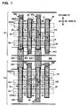
- Fig. 1 is a plan view schematically showing a layout of a semiconductor integrated circuit device including nonvolatile semiconductor memory devices obtained by the manufacturing method according to an embodiment of the present invention.
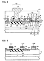
- Fig. 2 is a cross-sectional view schematically showing a section taken along the line A-A in Fig. 1.
- the above-described conventional nonvolatile semiconductor memory devices (memory cells) 100 are arranged in a matrix with a plurality of rows and columns, thereby making up a memory cell array.
- Fig. 1 shows a first block B1 and a second block B2 adjacent thereto.
- the first block B1 and the second block B2 are isolated by an element isolation region 300 extending in the row direction (X direction).
- a plurality of word lines 50 WL
- BL bit lines
- the word lines 50 are provided in contact with word gates 14.
- Impurity diffusion layers 16 and 18 form the bit lines 60.
- Each of first and second control gates 20 and 30 is formed of a conductive layer 40 extending in the column direction, specifically, along the sides of the word gate 14.
- the conductive layer 40 which forms the first and second control gates 20 and 30 is formed so as to enclose each of the impurity diffusion layers 16 and 18.
- One end of the first control gate 20 and one end of the second control gate 30 are connected and the other ends are connected to a common contact section 200. Therefore, as shown in Fig. 1, the common contact sections 200 are staggered relative to each other.
- the first and second control gates 20 and 30 have a function of a control gate for the memory cells and a function of interconnection which connects the control gates arranged in the column direction.
- Each memory cell 100 includes the word gate 14, the first control gate 20, the second control gate 30, the impurity diffusion layer 16 and the impurity diffusion layer 18.
- the impurity diffusion layers 16 and 18 are formed outside the first and second control gates 20 and 30.
- the adjacent memory cells 100 share the impurity diffusion layers 16 and 18.
- the impurity diffusion layers 16 are connected at the ends having no common contact section 200, by a contact impurity diffusion layer 400 formed in the semiconductor substrate.
- a contact 250 to the bit line 60 is formed on the contact impurity diffusion layer 400.
- the impurity diffusion layers 18 which are adjacent in the column direction are connected by a contact impurity diffusion layer (not shown) . Therefore, the contacts 250 are staggered relative to each other.
- the word gate 14 is formed on the main surface of a semiconductor substrate 10 with a first gate insulating layer 12 interposed.
- the impurity diffusion layers 16 and 18 are formed in the semiconductor substrate 10. Each of impurity diffusion layers 16 and 18 functions as a source region or a drain region.
- the first and second control gates 20 and 30 are formed on either side of the word gate 14 with a side insulating layer 24 interposed.
- the control gates are the same shape as sidewall insulating spacers in conventional MOS transistor.
- the semiconductor substrate 10 has an N-type first well 10a and a P-type second well 10b formed in the first well 10a.
- the first well 10a has a function of electrically isolating the second well 10b from other regions of the semiconductor substrate 10.
- the first control gate 20 is disposed on the second well 10b in the semiconductor substrate 10 with a second gate insulating layer 22 interposed, and disposed on one side of the word gate 14 with a side insulating layer 24 interposed.
- the second control gate 30 is disposed on the second well 10b in the semiconductor substrate 10 with the second gate insulating layer 22 interposed, and disposed on the other side of the word gate 14 with the side insulating layer 24 interposed.
- a first silicon oxide layer 22a, a silicon nitride layer 22b, and a second silicon oxide layer 22c make up the second gate insulating layer 22 and the side insulating layer 24.
- the second gate insulating layer 22 functions as a charge storage region.
- the first silicon oxide layer 22a mainly functions as a tunnel film through which carriers (electrons, for example) pass.
- the silicon nitride layer 22b mainly functions as a charge storage layer in which the carriers are trapped.
- the side insulating layers 24 formed on both sides of the word gate 14 have a function of electrically isolating the word gate 14 from the control gates 20 and 30.
- the side insulating layer 24 has such a function.
- the side insulating layer 24 and the second gate insulating layer 22 are formed in the same step and have the same layer structure.
- the side insulating layers 24 are formed so that the upper end thereof is located at a position higher than the upper ends of control gates 20 and 30 with respect to the semiconductor substrate 10.
- a buried insulating layer 70 is formed between the first control gate 20 and the second control gate 30 adjacent thereto. The buried insulating layer 70 covers the control gates 20 and 30 so that at least the control gates 20 and 30 are not exposed.
- the common contact section 200 applies a voltage to the control gates 20 and 30.
- the common contact section 200 includes an insulating layer 210, a conductive layer 220, and a cap layer 230 which are formed over the element isolation region 300.
- the insulating layer 210 is formed in the same step as the second gate insulating layer 22 and the side insulating layer 24.
- the insulating layer 210 is formed of a laminate consisting of the first silicon oxide layer 22a, the silicon nitride layer 22b, and the second silicon oxide layer 22c.
- the conductive layer 220 is formed in the same step as the first and second control gates 20 and 30.
- the conductive layer 220 is connected to the control gates 20 and 30 and formed of the same material as the control gates 20 and 30.
- the cap layer 230 is formed of an insulating layer such as a silicon nitride layer.
- the cap layer 230 functions as a mask layer (second mask layer) during patterning of the control gates 20 and 30 and the conductive layer 2
- An interlayer dielectric 72 is provided over the semiconductor substrate 10 on which the memory cells 100, the common contact sections 200, and the like are formed.
- the interlayer dielectric 72 has a contact hole which reaches the conductive layer 220 in the contact section 200, and this contact hole is filled with a conductive layer 82.
- the conductive layer 82 is connected to an interconnect layer 80 formed on the interlayer dielectric 72.
- every pair of control gates 20 and 30 in the shape of sidewalls is connected to the common contact section 200 in the shape of a pad, whereby an electrical connection with the control gates can be achieved reliably.
- the control gate of the present invention has a shape of sidewall and generally has a width of 0.1 ⁇ m or less. Therefore, it is important to secure an electrical connection with such control gates.
- electrical contact with the control gates can be secured by the common contact section in the minimum area.
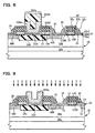
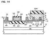
- FIG. 3 to 14 Each cross-sectional view is a section taken along the line A-A shown in Fig. 1.
- Figs. 3 to 14 components that are the same as those in Fig. 1 are denoted by the same reference numbers and further description is omitted.
- the interlayer dielectric 72 is formed by a conventional method, and then the conductive layers 82 and the interconnect layers 80 connected to the common contact sections 200 are formed, as shown in Fig. 2.
- the semiconductor integrated circuit device shown in Fig. 1 is fabricated by these steps.
- the common contact sections 200 can be formed together with the control gates 20 and 30 in the shape of sidewalls without increasing the number of steps.
- the common contact section 200 has a size close to at least the widths of the impurity diffusion layers 16 and 18, whereby a sufficiently large contact area can be secured. According to the present invention, therefore, reliable electrical connection with the control gates 20 and 30 can be achieved through the common contact sections 200 even if the control gates 20 and 30 are shaped as sidewalls for which it is difficult to provide a sufficient contact region.
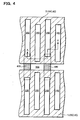
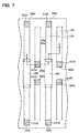
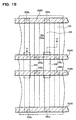
- Fig. 15 is a plan view showing the step (3) in the above embodiment and corresponds to Fig. 7.
- components that are the same as those shown in Fig. 7 are denoted by the same reference numbers, and further description thereof is omitted.
- the resist layers R100 are formed only in the regions corresponding to the common contact section formation regions 200a.
- the configuration in Fig. 15 has resist layers (first mask layers) R400 formed continuously so as to cover a plurality of common contact section formation regions 200a present in the row direction.
- resist layers (first mask layers) R400 formed continuously so as to cover a plurality of common contact section formation regions 200a present in the row direction.
- the doped polysilicon layer 20a (30a) remains in the area other than the common contact section formation regions 200a.
- unnecessary portions may be removed by using the cap layers (second mask layers) 230 as a mask when patterning the word gates 14 in the step (9) in the above embodiment.
- a bulk semiconductor substrate is used as a semiconductor layer in the above embodiment.
- a semiconductor layer of an SOI substrate may be used.
Landscapes
- Semiconductor Memories (AREA)
- Non-Volatile Memory (AREA)
Abstract
Description
in the step (i), the insulating layer which covers the first and second control gates may be provided by forming an insulating layer on the entire surface of the structure formed by the steps (a) to (h) and then removing the insulating layer by chemical mechanical polishing until the stopper layer is exposed. An insulating layer formed in this manner is hereinafter called a "buried insulating layer".
Claims (15)
- A method of manufacturing a semiconductor integrated circuit device including a memory cell array in which nonvolatile semiconductor memory devices are arranged in a matrix of a plurality of rows and columns, the method comprising the following steps (a) to (k):(a) a step of forming an element isolation region on the surface of a semiconductor layer;(b) a step of forming a first gate insulating layer and a laminate having a first conductive layer for a word gate disposed over the first gate insulating layer on the semiconductor layer, the laminate having a plurality of openings extending in a first direction;(c) a step of forming second gate insulating layers on the semiconductor layer so as to be adjacent to both sides of the first gate insulating layer;(d) a step of forming side insulating layers on both sides of the first conductive layer for the word gate;(e) a step of forming a second conductive layer over the entire surface of a structure formed by the steps (a) to (d) so as to cover the structure;(f) a step of forming a first mask layer on the second conductive layer at least in a region in which a common contact section is formed;(g) a step of forming a control gate and a common contact section which comprises:anisotropically etching the entire surface of the second conductive layer to form first and second control gates in the shape of sidewalls continuous in the first direction on either side of the side insulating layers, and to form a contact conductive layer at least in a region in which the common contact section is formed; andforming the contact conductive layer continuously with a pair of the first and second control gates adjacent in a second direction which intersects the first direction;(h) a step of doping the semiconductor layer located between the first and second control gates with impurities, and forming an impurity diffusion layer which forms a source region or a drain region;(i) a step of forming an insulating layer which covers the first and second control gates;(j) a step of forming a second mask layer in a region in which the common contact section is formed; and(k) a step of patterning the first conductive layer for the word gate.
- The method of manufacturing a semiconductor integrated circuit device as defined in claim 1,
wherein the second conductive layer for the control gate is formed of a doped polysilicon layer. - The method of manufacturing a semiconductor integrated circuit device as defined in claim 1 or 2,
wherein the second gate insulating layer is formed by depositing a first silicon oxide layer, a silicon nitride layer, and a second silicon oxide layer one after another. - The method of manufacturing a semiconductor integrated circuit device as defined in claim 3,
wherein the side insulating layers is formed in the same step as a step of forming the first silicon oxide layer, the silicon nitride layer, and the second silicon oxide layer. - The method of manufacturing a semiconductor integrated circuit device as defined in claim 3,
wherein the common contact section comprises an insulating layer formed on the semiconductor layer, and the insulating layer is formed in the same step as a step of forming the first silicon oxide layer, the silicon nitride layer, and the second silicon oxide layer. - The method of manufacturing a semiconductor integrated circuit device as defined in any one of claims 1 to 5,
wherein the step (b) comprises a step of forming a stopper layer for chemical mechanical polishing on the first conductive layer for the word gate, and
wherein in the step (i) , the insulating layer which covers the first and second control gates is provided by forming an insulating layer on the entire surface of the structure formed by the steps (a) to (h) and then removing the insulating layer by chemical mechanical polishing until the stopper layer is exposed. - The method of manufacturing a semiconductor integrated circuit device as defined in claim 6,
wherein the stopper layer is formed so that an upper surface thereof is located at a position higher than an upper end of the control gate. - The method of manufacturing a semiconductor integrated circuit device as defined in claim 7,
wherein the side insulating layers is formed so that an upper end thereof is located at the same level as an upper surface of the stopper layer. - The method of manufacturing a semiconductor integrated circuit device as defined in any one of claims 1 to 8,
wherein the common contact section is provided adjacent to an end of the impurity diffusion layer. - The method of manufacturing a semiconductor integrated circuit device as defined in claim 9,
wherein the common contact sections are staggered relative to each other. - The method of manufacturing a semiconductor integrated circuit device as defined in any one of claims 1 to 10,
wherein the memory cell array is divided into a plurality of blocks. - The method of manufacturing a semiconductor integrated circuit device as defined in claim 11,
wherein contact impurity diffusion layer is formed in the semiconductor layer after the step (a), and the impurity diffusion layer in one of the blocks is connected to the impurity diffusion layer in another one of the blocks adjacent to the one block through the contact impurity diffusion layer. - The method of manufacturing a semiconductor integrated circuit device as defined in any one of claims 1 to 12,
wherein the first mask layer is formed corresponding to a region in which the common contact section is formed in the step (f) . - The method of manufacturing a semiconductor integrated circuit device as defined in any one of claims 1 to 12,
wherein in the step (f), the first mask layer is formed continuously so as to cover regions in which a plurality of the common contact sections arranged in the second direction are formed. - The method of manufacturing a semiconductor integrated circuit device as defined in claim 14,
wherein in the step (g), a conductive layer is continuously formed so as to include regions in which the common contact sections are formed, by the first mask layer, and
wherein in the step (k), the contact conductive layer is formed together with the word gate by patterning the conductive layer together with the first conductive layer.
Applications Claiming Priority (2)
| Application Number | Priority Date | Filing Date | Title |
|---|---|---|---|
| JP2001021931 | 2001-01-30 | ||
| JP2001021931A JP4325972B2 (en) | 2001-01-30 | 2001-01-30 | Manufacturing method of semiconductor integrated circuit device including nonvolatile semiconductor memory device |
Publications (3)
| Publication Number | Publication Date |
|---|---|
| EP1227518A2 true EP1227518A2 (en) | 2002-07-31 |
| EP1227518A3 EP1227518A3 (en) | 2003-08-27 |
| EP1227518B1 EP1227518B1 (en) | 2009-06-24 |
Family
ID=18887409
Family Applications (1)
| Application Number | Title | Priority Date | Filing Date |
|---|---|---|---|
| EP02002105A Expired - Lifetime EP1227518B1 (en) | 2001-01-30 | 2002-01-28 | Method of manufacturing semiconductor integrated circuit device including nonvolatile semiconductor memory devices |
Country Status (8)
| Country | Link |
|---|---|
| US (1) | US6709922B2 (en) |
| EP (1) | EP1227518B1 (en) |
| JP (1) | JP4325972B2 (en) |
| KR (1) | KR100429954B1 (en) |
| CN (1) | CN1252813C (en) |
| AT (1) | ATE434834T1 (en) |
| DE (1) | DE60232693D1 (en) |
| TW (1) | TW530391B (en) |
Cited By (1)
| Publication number | Priority date | Publication date | Assignee | Title |
|---|---|---|---|---|
| CN113394225A (en) * | 2017-02-28 | 2021-09-14 | 东芝存储器株式会社 | Semiconductor device with a plurality of semiconductor chips |
Families Citing this family (46)
| Publication number | Priority date | Publication date | Assignee | Title |
|---|---|---|---|---|
| US6248633B1 (en) * | 1999-10-25 | 2001-06-19 | Halo Lsi Design & Device Technology, Inc. | Process for making and programming and operating a dual-bit multi-level ballistic MONOS memory |
| JP3671889B2 (en) | 2001-09-25 | 2005-07-13 | セイコーエプソン株式会社 | Semiconductor device and manufacturing method thereof |
| JP3674564B2 (en) * | 2001-09-25 | 2005-07-20 | セイコーエプソン株式会社 | Semiconductor device and manufacturing method thereof |
| US6897522B2 (en) * | 2001-10-31 | 2005-05-24 | Sandisk Corporation | Multi-state non-volatile integrated circuit memory systems that employ dielectric storage elements |
| US6925007B2 (en) * | 2001-10-31 | 2005-08-02 | Sandisk Corporation | Multi-state non-volatile integrated circuit memory systems that employ dielectric storage elements |
| JP3956709B2 (en) | 2002-01-23 | 2007-08-08 | セイコーエプソン株式会社 | Manufacturing method of semiconductor device |
| JP2003243616A (en) * | 2002-02-20 | 2003-08-29 | Seiko Epson Corp | Method for manufacturing semiconductor device |
| JP2003243618A (en) | 2002-02-20 | 2003-08-29 | Seiko Epson Corp | Method for manufacturing semiconductor device |
| JP3726760B2 (en) | 2002-02-20 | 2005-12-14 | セイコーエプソン株式会社 | Manufacturing method of semiconductor device |
| JP2003243617A (en) | 2002-02-20 | 2003-08-29 | Seiko Epson Corp | Method for manufacturing semiconductor device |
| JP2003258129A (en) * | 2002-03-01 | 2003-09-12 | Seiko Epson Corp | Manufacturing method of nonvolatile storage device |
| JP2003258132A (en) * | 2002-03-05 | 2003-09-12 | Seiko Epson Corp | Manufacturing method of nonvolatile storage device |
| JP2003258133A (en) * | 2002-03-05 | 2003-09-12 | Seiko Epson Corp | Method for manufacturing nonvolatile memory device and method for manufacturing semiconductor device |
| JP3640186B2 (en) * | 2002-03-06 | 2005-04-20 | セイコーエプソン株式会社 | Manufacturing method of semiconductor device |
| JP2003282744A (en) * | 2002-03-22 | 2003-10-03 | Seiko Epson Corp | Non-volatile storage device |
| JP3975349B2 (en) * | 2002-09-02 | 2007-09-12 | セイコーエプソン株式会社 | Semiconductor device and manufacturing method thereof |
| JP3975350B2 (en) * | 2002-09-11 | 2007-09-12 | セイコーエプソン株式会社 | Manufacturing method of semiconductor device |
| JP3972196B2 (en) * | 2002-09-18 | 2007-09-05 | セイコーエプソン株式会社 | Manufacturing method of semiconductor device |
| JP3743514B2 (en) * | 2002-10-24 | 2006-02-08 | セイコーエプソン株式会社 | Semiconductor device and manufacturing method thereof |
| US6888755B2 (en) * | 2002-10-28 | 2005-05-03 | Sandisk Corporation | Flash memory cell arrays having dual control gates per memory cell charge storage element |
| JP3664159B2 (en) * | 2002-10-29 | 2005-06-22 | セイコーエプソン株式会社 | Semiconductor device and manufacturing method thereof |
| JP3664160B2 (en) | 2002-10-30 | 2005-06-22 | セイコーエプソン株式会社 | Semiconductor device and manufacturing method thereof |
| JP3664161B2 (en) * | 2002-10-30 | 2005-06-22 | セイコーエプソン株式会社 | Semiconductor device and manufacturing method thereof |
| JP2004186452A (en) | 2002-12-04 | 2004-07-02 | Renesas Technology Corp | Nonvolatile semiconductor memory device and manufacturing method thereof |
| US20050251617A1 (en) * | 2004-05-07 | 2005-11-10 | Sinclair Alan W | Hybrid non-volatile memory system |
| US7518179B2 (en) * | 2004-10-08 | 2009-04-14 | Freescale Semiconductor, Inc. | Virtual ground memory array and method therefor |
| US7306552B2 (en) * | 2004-12-03 | 2007-12-11 | Samsung Electronics Co., Ltd. | Semiconductor device having load resistor and method of fabricating the same |
| JP4936659B2 (en) * | 2004-12-27 | 2012-05-23 | 株式会社東芝 | Manufacturing method of semiconductor device |
| JP4462424B2 (en) * | 2005-02-03 | 2010-05-12 | セイコーエプソン株式会社 | Semiconductor device |
| KR100629270B1 (en) * | 2005-02-23 | 2006-09-29 | 삼성전자주식회사 | NAND flash memory device and manufacturing method thereof |
| US7582929B2 (en) * | 2005-07-25 | 2009-09-01 | Freescale Semiconductor, Inc | Electronic device including discontinuous storage elements |
| US7112490B1 (en) * | 2005-07-25 | 2006-09-26 | Freescale Semiconductor, Inc. | Hot carrier injection programmable structure including discontinuous storage elements and spacer control gates in a trench |
| US7642594B2 (en) * | 2005-07-25 | 2010-01-05 | Freescale Semiconductor, Inc | Electronic device including gate lines, bit lines, or a combination thereof |
| US7619270B2 (en) * | 2005-07-25 | 2009-11-17 | Freescale Semiconductor, Inc. | Electronic device including discontinuous storage elements |
| US7619275B2 (en) * | 2005-07-25 | 2009-11-17 | Freescale Semiconductor, Inc. | Process for forming an electronic device including discontinuous storage elements |
| US7262997B2 (en) * | 2005-07-25 | 2007-08-28 | Freescale Semiconductor, Inc. | Process for operating an electronic device including a memory array and conductive lines |
| KR100668350B1 (en) * | 2005-12-20 | 2007-01-12 | 삼성전자주식회사 | NAND structured multi-bit nonvolatile memory device and manufacturing method thereof |
| US7592224B2 (en) | 2006-03-30 | 2009-09-22 | Freescale Semiconductor, Inc | Method of fabricating a storage device including decontinuous storage elements within and between trenches |
| US7951669B2 (en) * | 2006-04-13 | 2011-05-31 | Sandisk Corporation | Methods of making flash memory cell arrays having dual control gates per memory cell charge storage element |
| FR2901723B1 (en) * | 2006-06-06 | 2008-07-04 | Commissariat Energie Atomique | ASSEMBLY AND METHOD FOR BRAZING ASSEMBLY OF OBJECT AND SUPPORT |
| KR100773356B1 (en) * | 2006-11-07 | 2007-11-05 | 삼성전자주식회사 | Non-volatile Memory Device Having Separate Charge Storage Patterns and Manufacturing Method Thereof |
| US7572699B2 (en) * | 2007-01-24 | 2009-08-11 | Freescale Semiconductor, Inc | Process of forming an electronic device including fins and discontinuous storage elements |
| US7838922B2 (en) * | 2007-01-24 | 2010-11-23 | Freescale Semiconductor, Inc. | Electronic device including trenches and discontinuous storage elements |
| US7651916B2 (en) * | 2007-01-24 | 2010-01-26 | Freescale Semiconductor, Inc | Electronic device including trenches and discontinuous storage elements and processes of forming and using the same |
| TWI478293B (en) * | 2011-05-16 | 2015-03-21 | Promos Technologies Inc | Method of fabricating non-volatile memory device |
| US9735245B2 (en) * | 2014-08-25 | 2017-08-15 | Taiwan Semiconductor Manufacturing Co., Ltd. | Recessed salicide structure to integrate a flash memory device with a high κ, metal gate logic device |
Family Cites Families (16)
| Publication number | Priority date | Publication date | Assignee | Title |
|---|---|---|---|---|
| JP3059442B2 (en) * | 1988-11-09 | 2000-07-04 | 株式会社日立製作所 | Semiconductor storage device |
| JPH05326976A (en) | 1992-05-20 | 1993-12-10 | Rohm Co Ltd | Semiconductor memory and manufacture thereof |
| JPH07161851A (en) | 1993-12-10 | 1995-06-23 | Sony Corp | Semiconductor nonvolatile memory device and manufacturing method thereof |
| US5408115A (en) * | 1994-04-04 | 1995-04-18 | Motorola Inc. | Self-aligned, split-gate EEPROM device |
| US5422504A (en) | 1994-05-02 | 1995-06-06 | Motorola Inc. | EEPROM memory device having a sidewall spacer floating gate electrode and process |
| JP2658907B2 (en) * | 1994-09-29 | 1997-09-30 | 日本電気株式会社 | Nonvolatile semiconductor memory device and method of manufacturing the same |
| US5969383A (en) | 1997-06-16 | 1999-10-19 | Motorola, Inc. | Split-gate memory device and method for accessing the same |
| JP2978477B1 (en) | 1998-06-12 | 1999-11-15 | 株式会社日立製作所 | Semiconductor integrated circuit device and method of manufacturing the same |
| KR100316709B1 (en) * | 1998-07-13 | 2001-12-12 | 윤종용 | Fabrication method of non-volatile memory device |
| JP3973819B2 (en) | 1999-03-08 | 2007-09-12 | 株式会社東芝 | Semiconductor memory device and manufacturing method thereof |
| US6255166B1 (en) | 1999-08-05 | 2001-07-03 | Aalo Lsi Design & Device Technology, Inc. | Nonvolatile memory cell, method of programming the same and nonvolatile memory array |
| US6177318B1 (en) | 1999-10-18 | 2001-01-23 | Halo Lsi Design & Device Technology, Inc. | Integration method for sidewall split gate monos transistor |
| US6248633B1 (en) | 1999-10-25 | 2001-06-19 | Halo Lsi Design & Device Technology, Inc. | Process for making and programming and operating a dual-bit multi-level ballistic MONOS memory |
| JP4904631B2 (en) | 2000-10-27 | 2012-03-28 | ソニー株式会社 | Nonvolatile semiconductor memory device and manufacturing method thereof |
| US6518124B1 (en) * | 2001-09-18 | 2003-02-11 | Seiko Epson Corporation | Method of fabricating semiconductor device |
| US6413821B1 (en) * | 2001-09-18 | 2002-07-02 | Seiko Epson Corporation | Method of fabricating semiconductor device including nonvolatile memory and peripheral circuit |
-
2001
- 2001-01-30 JP JP2001021931A patent/JP4325972B2/en not_active Expired - Fee Related
-
2002
- 2002-01-23 US US10/052,255 patent/US6709922B2/en not_active Expired - Fee Related
- 2002-01-28 AT AT02002105T patent/ATE434834T1/en not_active IP Right Cessation
- 2002-01-28 DE DE60232693T patent/DE60232693D1/en not_active Expired - Lifetime
- 2002-01-28 EP EP02002105A patent/EP1227518B1/en not_active Expired - Lifetime
- 2002-01-28 TW TW091101398A patent/TW530391B/en not_active IP Right Cessation
- 2002-01-29 KR KR10-2002-0005126A patent/KR100429954B1/en not_active Expired - Fee Related
- 2002-01-30 CN CNB02103205XA patent/CN1252813C/en not_active Expired - Fee Related
Cited By (2)
| Publication number | Priority date | Publication date | Assignee | Title |
|---|---|---|---|---|
| CN113394225A (en) * | 2017-02-28 | 2021-09-14 | 东芝存储器株式会社 | Semiconductor device with a plurality of semiconductor chips |
| CN113394225B (en) * | 2017-02-28 | 2023-11-21 | 铠侠股份有限公司 | Semiconductor device |
Also Published As
| Publication number | Publication date |
|---|---|
| EP1227518A3 (en) | 2003-08-27 |
| US20020127805A1 (en) | 2002-09-12 |
| US6709922B2 (en) | 2004-03-23 |
| JP4325972B2 (en) | 2009-09-02 |
| EP1227518B1 (en) | 2009-06-24 |
| CN1252813C (en) | 2006-04-19 |
| TW530391B (en) | 2003-05-01 |
| ATE434834T1 (en) | 2009-07-15 |
| DE60232693D1 (en) | 2009-08-06 |
| KR100429954B1 (en) | 2004-05-03 |
| CN1369908A (en) | 2002-09-18 |
| KR20020063825A (en) | 2002-08-05 |
| JP2002231831A (en) | 2002-08-16 |
Similar Documents
| Publication | Publication Date | Title |
|---|---|---|
| EP1227518B1 (en) | Method of manufacturing semiconductor integrated circuit device including nonvolatile semiconductor memory devices | |
| US6809385B2 (en) | Semiconductor integrated circuit device including nonvolatile semiconductor memory devices having control gates connected to common contact section | |
| US6891271B2 (en) | Non-volatile memory device | |
| US6413821B1 (en) | Method of fabricating semiconductor device including nonvolatile memory and peripheral circuit | |
| US6518124B1 (en) | Method of fabricating semiconductor device | |
| JP3726760B2 (en) | Manufacturing method of semiconductor device | |
| US6995420B2 (en) | Semiconductor device and method of manufacturing the same | |
| US20070155087A1 (en) | Method of manufacturing split gate flash memory | |
| US6812520B2 (en) | Semiconductor device and method of manufacturing the same | |
| JP3531641B2 (en) | Method for manufacturing semiconductor device | |
| JP2003243618A (en) | Method for manufacturing semiconductor device | |
| US6737322B2 (en) | Method for manufacturing semiconductor device | |
| JP2003218240A (en) | Method for manufacturing semiconductor device | |
| JP3812645B2 (en) | Semiconductor device | |
| JP2003243617A (en) | Method for manufacturing semiconductor device | |
| JP2003218244A (en) | Method for manufacturing semiconductor device | |
| US6894361B2 (en) | Semiconductor device | |
| JP2003243616A (en) | Method for manufacturing semiconductor device | |
| JP2004047802A (en) | Method for manufacturing semiconductor device |
Legal Events
| Date | Code | Title | Description |
|---|---|---|---|
| PUAI | Public reference made under article 153(3) epc to a published international application that has entered the european phase |
Free format text: ORIGINAL CODE: 0009012 |
|
| AK | Designated contracting states |
Kind code of ref document: A2 Designated state(s): AT BE CH CY DE DK ES FI FR GB GR IE IT LI LU MC NL PT SE TR |
|
| AX | Request for extension of the european patent |
Free format text: AL;LT;LV;MK;RO;SI |
|
| PUAL | Search report despatched |
Free format text: ORIGINAL CODE: 0009013 |
|
| AK | Designated contracting states |
Designated state(s): AT BE CH CY DE DK ES FI FR GB GR IE IT LI LU MC NL PT SE TR |
|
| AX | Request for extension of the european patent |
Extension state: AL LT LV MK RO SI |
|
| RIC1 | Information provided on ipc code assigned before grant |
Ipc: 7H 01L 27/115 A Ipc: 7H 01L 29/792 B Ipc: 7H 01L 21/8246 B Ipc: 7H 01L 21/28 B |
|
| 17P | Request for examination filed |
Effective date: 20030825 |
|
| AKX | Designation fees paid |
Designated state(s): AT BE CH CY DE DK ES FI FR GB GR IE IT LI LU MC NL PT SE TR |
|
| RAP1 | Party data changed (applicant data changed or rights of an application transferred) |
Owner name: SEIKO EPSON CORPORATION |
|
| GRAP | Despatch of communication of intention to grant a patent |
Free format text: ORIGINAL CODE: EPIDOSNIGR1 |
|
| GRAS | Grant fee paid |
Free format text: ORIGINAL CODE: EPIDOSNIGR3 |
|
| GRAA | (expected) grant |
Free format text: ORIGINAL CODE: 0009210 |
|
| AK | Designated contracting states |
Kind code of ref document: B1 Designated state(s): AT BE CH CY DE DK ES FI FR GB GR IE IT LI LU MC NL PT SE TR |
|
| REG | Reference to a national code |
Ref country code: GB Ref legal event code: FG4D |
|
| REG | Reference to a national code |
Ref country code: CH Ref legal event code: EP |
|
| REG | Reference to a national code |
Ref country code: IE Ref legal event code: FG4D |
|
| REF | Corresponds to: |
Ref document number: 60232693 Country of ref document: DE Date of ref document: 20090806 Kind code of ref document: P |
|
| PG25 | Lapsed in a contracting state [announced via postgrant information from national office to epo] |
Ref country code: AT Free format text: LAPSE BECAUSE OF FAILURE TO SUBMIT A TRANSLATION OF THE DESCRIPTION OR TO PAY THE FEE WITHIN THE PRESCRIBED TIME-LIMIT Effective date: 20090624 Ref country code: FI Free format text: LAPSE BECAUSE OF FAILURE TO SUBMIT A TRANSLATION OF THE DESCRIPTION OR TO PAY THE FEE WITHIN THE PRESCRIBED TIME-LIMIT Effective date: 20090624 |
|
| PG25 | Lapsed in a contracting state [announced via postgrant information from national office to epo] |
Ref country code: SE Free format text: LAPSE BECAUSE OF FAILURE TO SUBMIT A TRANSLATION OF THE DESCRIPTION OR TO PAY THE FEE WITHIN THE PRESCRIBED TIME-LIMIT Effective date: 20090924 |
|
| NLV1 | Nl: lapsed or annulled due to failure to fulfill the requirements of art. 29p and 29m of the patents act | ||
| PG25 | Lapsed in a contracting state [announced via postgrant information from national office to epo] |
Ref country code: ES Free format text: LAPSE BECAUSE OF FAILURE TO SUBMIT A TRANSLATION OF THE DESCRIPTION OR TO PAY THE FEE WITHIN THE PRESCRIBED TIME-LIMIT Effective date: 20091005 |
|
| PG25 | Lapsed in a contracting state [announced via postgrant information from national office to epo] |
Ref country code: BE Free format text: LAPSE BECAUSE OF FAILURE TO SUBMIT A TRANSLATION OF THE DESCRIPTION OR TO PAY THE FEE WITHIN THE PRESCRIBED TIME-LIMIT Effective date: 20090624 Ref country code: NL Free format text: LAPSE BECAUSE OF FAILURE TO SUBMIT A TRANSLATION OF THE DESCRIPTION OR TO PAY THE FEE WITHIN THE PRESCRIBED TIME-LIMIT Effective date: 20090624 |
|
| PG25 | Lapsed in a contracting state [announced via postgrant information from national office to epo] |
Ref country code: PT Free format text: LAPSE BECAUSE OF FAILURE TO SUBMIT A TRANSLATION OF THE DESCRIPTION OR TO PAY THE FEE WITHIN THE PRESCRIBED TIME-LIMIT Effective date: 20091024 |
|
| PG25 | Lapsed in a contracting state [announced via postgrant information from national office to epo] |
Ref country code: DK Free format text: LAPSE BECAUSE OF FAILURE TO SUBMIT A TRANSLATION OF THE DESCRIPTION OR TO PAY THE FEE WITHIN THE PRESCRIBED TIME-LIMIT Effective date: 20090624 |
|
| PLBE | No opposition filed within time limit |
Free format text: ORIGINAL CODE: 0009261 |
|
| STAA | Information on the status of an ep patent application or granted ep patent |
Free format text: STATUS: NO OPPOSITION FILED WITHIN TIME LIMIT |
|
| 26N | No opposition filed |
Effective date: 20100325 |
|
| PG25 | Lapsed in a contracting state [announced via postgrant information from national office to epo] |
Ref country code: MC Free format text: LAPSE BECAUSE OF NON-PAYMENT OF DUE FEES Effective date: 20100131 |
|
| REG | Reference to a national code |
Ref country code: CH Ref legal event code: PL |
|
| PG25 | Lapsed in a contracting state [announced via postgrant information from national office to epo] |
Ref country code: LI Free format text: LAPSE BECAUSE OF NON-PAYMENT OF DUE FEES Effective date: 20100131 Ref country code: CH Free format text: LAPSE BECAUSE OF NON-PAYMENT OF DUE FEES Effective date: 20100131 Ref country code: GR Free format text: LAPSE BECAUSE OF FAILURE TO SUBMIT A TRANSLATION OF THE DESCRIPTION OR TO PAY THE FEE WITHIN THE PRESCRIBED TIME-LIMIT Effective date: 20090925 |
|
| PG25 | Lapsed in a contracting state [announced via postgrant information from national office to epo] |
Ref country code: IE Free format text: LAPSE BECAUSE OF NON-PAYMENT OF DUE FEES Effective date: 20100128 |
|
| PG25 | Lapsed in a contracting state [announced via postgrant information from national office to epo] |
Ref country code: IT Free format text: LAPSE BECAUSE OF FAILURE TO SUBMIT A TRANSLATION OF THE DESCRIPTION OR TO PAY THE FEE WITHIN THE PRESCRIBED TIME-LIMIT Effective date: 20090624 |
|
| PGFP | Annual fee paid to national office [announced via postgrant information from national office to epo] |
Ref country code: FR Payment date: 20120202 Year of fee payment: 11 |
|
| PGFP | Annual fee paid to national office [announced via postgrant information from national office to epo] |
Ref country code: DE Payment date: 20120125 Year of fee payment: 11 |
|
| PGFP | Annual fee paid to national office [announced via postgrant information from national office to epo] |
Ref country code: GB Payment date: 20120125 Year of fee payment: 11 |
|
| PG25 | Lapsed in a contracting state [announced via postgrant information from national office to epo] |
Ref country code: CY Free format text: LAPSE BECAUSE OF FAILURE TO SUBMIT A TRANSLATION OF THE DESCRIPTION OR TO PAY THE FEE WITHIN THE PRESCRIBED TIME-LIMIT Effective date: 20090624 |
|
| PG25 | Lapsed in a contracting state [announced via postgrant information from national office to epo] |
Ref country code: LU Free format text: LAPSE BECAUSE OF NON-PAYMENT OF DUE FEES Effective date: 20100128 |
|
| PG25 | Lapsed in a contracting state [announced via postgrant information from national office to epo] |
Ref country code: TR Free format text: LAPSE BECAUSE OF FAILURE TO SUBMIT A TRANSLATION OF THE DESCRIPTION OR TO PAY THE FEE WITHIN THE PRESCRIBED TIME-LIMIT Effective date: 20090624 |
|
| GBPC | Gb: european patent ceased through non-payment of renewal fee |
Effective date: 20130128 |
|
| REG | Reference to a national code |
Ref country code: FR Ref legal event code: ST Effective date: 20130930 |
|
| PG25 | Lapsed in a contracting state [announced via postgrant information from national office to epo] |
Ref country code: DE Free format text: LAPSE BECAUSE OF NON-PAYMENT OF DUE FEES Effective date: 20130801 |
|
| REG | Reference to a national code |
Ref country code: DE Ref legal event code: R119 Ref document number: 60232693 Country of ref document: DE Effective date: 20130801 |
|
| PG25 | Lapsed in a contracting state [announced via postgrant information from national office to epo] |
Ref country code: GB Free format text: LAPSE BECAUSE OF NON-PAYMENT OF DUE FEES Effective date: 20130128 Ref country code: FR Free format text: LAPSE BECAUSE OF NON-PAYMENT OF DUE FEES Effective date: 20130131 |