EP1227515A2 - Buried type capacitor for integrated circuits - Google Patents
Buried type capacitor for integrated circuits Download PDFInfo
- Publication number
- EP1227515A2 EP1227515A2 EP02250519A EP02250519A EP1227515A2 EP 1227515 A2 EP1227515 A2 EP 1227515A2 EP 02250519 A EP02250519 A EP 02250519A EP 02250519 A EP02250519 A EP 02250519A EP 1227515 A2 EP1227515 A2 EP 1227515A2
- Authority
- EP
- European Patent Office
- Prior art keywords
- semiconductor device
- semiconductor
- cavity
- substrate
- capacitor
- Prior art date
- Legal status (The legal status is an assumption and is not a legal conclusion. Google has not performed a legal analysis and makes no representation as to the accuracy of the status listed.)
- Withdrawn
Links
- 239000003990 capacitor Substances 0.000 title claims abstract description 79
- 239000004065 semiconductor Substances 0.000 claims abstract description 133
- 239000000758 substrate Substances 0.000 claims abstract description 69
- 238000005530 etching Methods 0.000 claims description 6
- 238000002161 passivation Methods 0.000 claims description 5
- 238000009966 trimming Methods 0.000 claims description 5
- 238000007736 thin film deposition technique Methods 0.000 claims description 3
- 239000012212 insulator Substances 0.000 claims description 2
- 230000000149 penetrating effect Effects 0.000 claims description 2
- 238000000034 method Methods 0.000 description 22
- XUIMIQQOPSSXEZ-UHFFFAOYSA-N Silicon Chemical compound [Si] XUIMIQQOPSSXEZ-UHFFFAOYSA-N 0.000 description 15
- 229910052710 silicon Inorganic materials 0.000 description 15
- 239000010703 silicon Substances 0.000 description 15
- VYPSYNLAJGMNEJ-UHFFFAOYSA-N Silicium dioxide Chemical compound O=[Si]=O VYPSYNLAJGMNEJ-UHFFFAOYSA-N 0.000 description 12
- 238000005516 engineering process Methods 0.000 description 11
- 239000000463 material Substances 0.000 description 11
- 239000010408 film Substances 0.000 description 10
- 239000004642 Polyimide Substances 0.000 description 7
- 238000004519 manufacturing process Methods 0.000 description 7
- 229920001721 polyimide Polymers 0.000 description 7
- 235000012431 wafers Nutrition 0.000 description 7
- JBRZTFJDHDCESZ-UHFFFAOYSA-N AsGa Chemical compound [As]#[Ga] JBRZTFJDHDCESZ-UHFFFAOYSA-N 0.000 description 6
- 229910001218 Gallium arsenide Inorganic materials 0.000 description 6
- 238000013461 design Methods 0.000 description 5
- 239000000377 silicon dioxide Substances 0.000 description 5
- 238000000151 deposition Methods 0.000 description 3
- 230000008021 deposition Effects 0.000 description 3
- 238000010422 painting Methods 0.000 description 3
- 239000003566 sealing material Substances 0.000 description 3
- 229910000679 solder Inorganic materials 0.000 description 3
- 238000004528 spin coating Methods 0.000 description 3
- 238000004544 sputter deposition Methods 0.000 description 3
- 239000010409 thin film Substances 0.000 description 3
- 239000000470 constituent Substances 0.000 description 2
- 238000010586 diagram Methods 0.000 description 2
- 239000003989 dielectric material Substances 0.000 description 2
- 230000006870 function Effects 0.000 description 2
- 229910052751 metal Inorganic materials 0.000 description 2
- 239000002184 metal Substances 0.000 description 2
- 238000001020 plasma etching Methods 0.000 description 2
- 235000012239 silicon dioxide Nutrition 0.000 description 2
- 229910052814 silicon oxide Inorganic materials 0.000 description 2
- RYGMFSIKBFXOCR-UHFFFAOYSA-N Copper Chemical compound [Cu] RYGMFSIKBFXOCR-UHFFFAOYSA-N 0.000 description 1
- GYHNNYVSQQEPJS-UHFFFAOYSA-N Gallium Chemical compound [Ga] GYHNNYVSQQEPJS-UHFFFAOYSA-N 0.000 description 1
- 229910052782 aluminium Inorganic materials 0.000 description 1
- XAGFODPZIPBFFR-UHFFFAOYSA-N aluminium Chemical compound [Al] XAGFODPZIPBFFR-UHFFFAOYSA-N 0.000 description 1
- 230000015572 biosynthetic process Effects 0.000 description 1
- 229910052802 copper Inorganic materials 0.000 description 1
- 239000010949 copper Substances 0.000 description 1
- 238000011161 development Methods 0.000 description 1
- 238000009826 distribution Methods 0.000 description 1
- 239000012777 electrically insulating material Substances 0.000 description 1
- -1 etc. Substances 0.000 description 1
- 230000002349 favourable effect Effects 0.000 description 1
- 229910052733 gallium Inorganic materials 0.000 description 1
- 238000005304 joining Methods 0.000 description 1
- 238000010030 laminating Methods 0.000 description 1
- 238000004806 packaging method and process Methods 0.000 description 1
- 238000000059 patterning Methods 0.000 description 1
- 238000012545 processing Methods 0.000 description 1
- 230000001681 protective effect Effects 0.000 description 1
- 238000005488 sandblasting Methods 0.000 description 1
- 238000000427 thin-film deposition Methods 0.000 description 1
- 238000012546 transfer Methods 0.000 description 1
Images


Classifications
-
- H—ELECTRICITY
- H10—SEMICONDUCTOR DEVICES; ELECTRIC SOLID-STATE DEVICES NOT OTHERWISE PROVIDED FOR
- H10D—INORGANIC ELECTRIC SEMICONDUCTOR DEVICES
- H10D48/00—Individual devices not covered by groups H10D1/00 - H10D44/00
- H10D48/01—Manufacture or treatment
-
- H—ELECTRICITY
- H10—SEMICONDUCTOR DEVICES; ELECTRIC SOLID-STATE DEVICES NOT OTHERWISE PROVIDED FOR
- H10D—INORGANIC ELECTRIC SEMICONDUCTOR DEVICES
- H10D89/00—Aspects of integrated devices not covered by groups H10D84/00 - H10D88/00
- H10D89/60—Integrated devices comprising arrangements for electrical or thermal protection, e.g. protection circuits against electrostatic discharge [ESD]
Definitions
- the present invention relates to a semiconductor device employed in DSPs (digital signal micro processors), CPUs (central processing units), memory devices, computer memory, etc., for electronic devices such as computers; and in further detail, it relates to a semiconductor device equipped with a capacitor buried in a semiconductor substrate made from silicon etc.
- DSPs digital signal micro processors
- CPUs central processing units
- memory devices computer memory, etc.
- semiconductor device equipped with a capacitor buried in a semiconductor substrate made from silicon etc.
- DSP Digital Signal Processor
- MPU Micro Processor Unit
- RAM Random Access Memory
- wire bonding method is employed in connecting each of the bonding pads (pads for drawing external electrodes), which are provided to the periphery of the surface of the device, with each of the lead electrodes of the lead frame.
- wireless bonding methods forming joints without using wires, and among them, frequently employed are a flip-chip method using solders, bumps, etc., and a TAB method using bump tapes, etc.
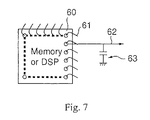
- Fig. 7 is given a schematically shown external appearance of a DRAM device and a DSP device (60) as examples of semiconductor devices known in the art.
- a signal line is shown by an arrowhead ( ⁇ ) 62, which is externally connected with a chip capacitor (decoupling capacitor) 63, etc.
- a bonding wire 61 is disposed outward from the periphery of the device 60. Shown aligned herein are plural bonding wires connected to the outside.
- the present invention has been made in the light of the aforementioned problems of the semiconductor devices known heretofore described above, and a great improvement is made on the structure and the method of producing the semiconductor device.
- the invention provides a key technology for such semiconductor devices, and an object of the present invention is to provide a semiconductor device capable of sufficiently satisfying requirements for future devices such as higher control speed, larger memory capacity, and higher stability in performance; hence, it relates to a semiconductor device equipped with a buried type capacitor that is formed by directly burying it in a semiconductor substrate (a wafer) made of a material such as silicon and gallium, and the invention further includes a particularly useful interconnection technology also useful for semiconductor devices comprising a laminate module (constitution element) having multiple layers on a semiconductor base body or a bare die (exposed chip body), which attains a high precision layer structure and assembly process therefor in semiconductor devices made from materials such as silicon and GaAs.
- the semiconductor device according to the present invention utilizes means as follows.
- the attached symbols are in conformity with those shown in the drawings.
- Fig.1 shows a cross section constitutional view of semiconductor base bodies (101, 102, 103) of a semiconductor device according to the present invention.
- (a) shows a capacitor structure in which the bottom portion of a cavity 11 is provided inside the substrate 10 and not penetrating
- (b) shows a capacitor structure in which the first electrode layer (the first metallic layer) provided to the bottom portion side of the cavity 11 is exposed
- (C) shows a capacitor structure in which the cavity has an approximately U-shaped cross section, wherein electrodes ( ⁇ 1 and ⁇ 2) are provided to the first electrode layer (first metallic layer), and an electrode ( ⁇ 1) is provided to the second electrode layer (second metallic layer).
- Fig. 2 shows an example of a semiconductor device according to the present invention, and provides a cross section view and an upper plan view showing the structure in which a first electrode layer 13 (Ti/W layer, etc.) is formed on the cavity 11.
- a first electrode layer 13 Ti/W layer, etc.
- Fig. 3 shows a semiconductor chip according to an example of a semiconductor device according to the present invention, and is an upper plan view showing a constitution in which a plurality of connection pads (I/O pads) are arranged in the periphery.
- Fig. 4 shows an example of the flow of manufacture processes of a semiconductor base body of a semiconductor device according to the present invention, and it provides the process steps showing the procedure of forming a cavity and a capacitor part having a laminate structure.
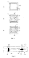
- Fig. 5 shows an arrangement structure showing various arrangements of the capacitor part having a capacitor layered structure in a semiconductor device according to the present invention, wherein (a) is an example in which a plurality of capacitors A are arranged in the periphery of the semiconductor substrate 10, (b) is an example of an arrangement in which the capacitor part A is connected to power source, GND, and signal line, and (c) is an example of an arrangement in which the capacitor part A is connected to a clock line.
- Fig. 6 refers to a semiconductor device according to the present invention, and it provides a cross section of an explanatory structure view of interconnection of a plurality of semiconductor base bodies (110, 111) by using ball bodies (120, 121).
- Fig. 7 shows an example of a semiconductor device of a conventional type, and is a schematically drawn outer appearance of a DRAM or a DSP device (60).
- Fig. 1 is given a cross section view of the constitution showing the semiconductor base bodies (101, 102, 103) constituting the semiconductor device according to the present invention.
- a cavity 11 is formed on the surface of a substrate 10, and the bottom portion of the cavity 11 is inside the substrate 10.
- Fig. 1 (b) shows a structure in which a means such as etching is applied from the back (bottom) surface of the substrate 10, so that the substrate material is removed, making the substrate thinner in such a manner that the first electrode layer (the first metallic layer) is exposed on the back plane (bottom plane) side of the cavity 11.
- Fig. 11 (c) shows a capacitor structure having an approximately U shaped cross section, in which electrodes ( ⁇ 1 and ⁇ 2) are formed on the first electrode layer (first metallic layer) and an electrode ( ⁇ 1) is formed on the second electrode layer (second metallic layer).
- the cavity 11 formed inside the semiconductor substrate 10 has a three-dimensional structure.
- a truncated cone shape as shown in the figure, but the shape need not be limited thereto.
- various types of three-dimensional shapes such as a reverse truncated cone shape, cylindrical shape, dish shape, pot shape, bowl shape, vase shape, conical shape, etc.
- shapes such as circular, ellipsoidal, polygonal, and asymmetrical shapes as desired.
- the cavity 11 is of a structure having an aperture or an opening on the substrate 10 (device surface); the enlarged diameter side of the cavity shape has its aperture opened at the surface of the substrate 10, while the shorter diameter side forms a concave shape inside the substrate.
- the entire cavity is shown with an approximately truncated cone shape (reversed conical shape).
- the three-dimensional morphology not only is limited thereto, but also can have an aperture on the surface of the substrate 10 having a diameter smaller than the lateral diameter of the cavity provided inside the substrate.
- a bucket-like morphology or a reversed bucket-like morphology there can be provided a triangular flask morphology or a reversed triangular flask morphology.
- straight and cylindrical or square trench shaped cavity structures constant in width which are well known for being the cavity structure of a memory employed in a conventional DRAM device, etc., may be employed as well.
- the cavity 11 comprises, in the concave portion provided to the inner plane thereof, a capacitor part A equipped with a capacitor structure buried in the substrate 10. Firstly, a cavity 11 is formed on the surface of the semiconductor substrate 10 by means of plasma etching, etc. Then, in a passivation process, a silicon dioxide (SiO 2 ) film 12 is formed on the surface of the semiconductor substrate 10 and on the inner surface of the cavity 11.
- SiO 2 silicon dioxide
- a first electrode layer 13 (such as Ti/W layer, etc.) is formed in the cavity 11 by means of a thin film deposition method suchas CVD, sputtering, electric deposition, spin coating, painting, etc., and then, a dielectric layer 14 is laminated thereon by using a dielectric material such as polyimide (PI). Further thereon, a second electrode layer 15 is formed laminated thereon to complete a multilayered laminate structure for capacitor part A.
- a capacitor part having a laminate structure formed by repeating the process steps of forming the first electrode layer 13 through the second electrode layer 15 may be provided.
- the cavity substrate surface prior to the formation of the first electrode layer 13 or the first electrode layer itself may be surface roughened by means such as sandblasting or etching to increase the area of the capacitance carrying surface, and the dielectric layer 14 and the second electrode layer 15 may be formed thereon, such that the capacitance of the capacitor formed inside the cavity may be increased.
- a sealing material 16 such as polyimide, etc., or a metal, etc.
- a sealing material 16 such as polyimide, etc., or a metal, etc.
- an electrically insulating material is used as the sealing material 16 at the surface in contact with the second electrode layer 15, but it may be formed otherwise by incorporating an insulating film or an insulating layer.
- Fig. 1 (c) is shown another example (semiconductor base body 103) of a semiconductor device according to the present invention.
- the cavity 11 used herein is provided in morphology as such similar to a U-shaped cross section or a vase-like shape, such that the bottom is provided with an edge-free round shape.
- a capacitor part A having a multilayered laminate structure comprising a first electrode layer 13 (e.g., a Ti/W layer, etc.), a dielectric layer 14 (made of polyimide, etc.), and a second electrode layer 15, and furthermore, the first electrode layer 13 comprises an electrode ⁇ 1 on the front surface and an electrode ⁇ 2 on the back side, and the second electrode layer 15 comprises an electrode ⁇ 1 on the front surface.
- the capacitor function of the present invention can be realized by taking ⁇ 1 and ⁇ 1 as electrodes, or ⁇ 2 and ⁇ 1 as electrodes.
- S represents the area of the electrode
- D represents the thickness of the dielectric (distance between the electrodes)
- ⁇ represents the dielectric constant of the dielectric.
- a semiconductor device showing the cross section view and the upper plan view of a structure comprising a first electrode layer 13 (e.g., Ti/W layer, etc.) formed inside a cavity 11.
- the cavity 11 is formed on a substrate 10, and, in a passivation process, a silicon dioxide (SiO 2 ) film 12 is formed on the surface of the semiconductor substrate 10 and on the inner surface of the cavity 11.
- the first electrode layer 13 is formed in such a manner that it may continuously cover both the inner surface of the cavity 11 and the substrate surface at the periphery of the cavity.
- the shape of the first electrode layer 13 herein is not only limited to a rectangle or a square as shown in Fig. 2, but may be of any shape such as circle or oval.
- the depth of the cavity 11 herein may be set approximately equal to the thickness n of the substrate 10 as shown in Fig. 2, because the metallic layer 13' (i.e., the first electrode layer 13) is exposed from the back of the substrate 11.
- Fig. 3 is shown an upper planar view of a semiconductor chip according to an example of the semiconductor device of the present invention.
- a silicon substrate 10' is connected in contact with a chip substrate 20, and a pad portion (e.g., 21, 22, etc.) is provided to the periphery thereof.
- a plurality of pad portions for external connection are arranged on the periphery of the silicon substrate 10'.
- the pad portions e.g., 21, 22, etc.
- the pad portions can be formed as capacitors with structure according to the present invention.
- the structure is provided as such that the capacitor electrodes may be taken from the front side (e.g., ⁇ 1 and ⁇ 2), or one electrode each taken from the front and the back sides (e.g., ⁇ 2 and ⁇ 1) of the substrate.
- the electrode (bonding pad) provided to the periphery of the IC chip surface can be connected simply to the lead frame, and this largely contributes to the realization of efficient design, reduced product size, etc., thereby leading to the production of a product matching the market needs.
- Figure 4 is related to the production of a semiconductor device according to the present invention, and shows an example of the process steps for forming a cavity and a capacitor part according to the capacitor laminated structure.
- Fig. 5 is an structure diagram showing various types of arrangements of a capacitor part A having a capacitor laminate structure of the semiconductor device according to the present invention.
- filled circle represents an I/O pad (A) comprising a capacitor part in which the capacitor structure according to the present invention is applied
- open circle represents an I/O pad (C) of a conventional type having no capacitor part according to the present invention.
- the I/O pad (filled circle) (A) according to the present invention may be properly and freely used in combination with the conventional I/O pad (open circle) (C) and arranged on the semiconductor substrate to constitute various types of semiconductor devices.
- the semiconductor substrate as a matter of course, used are not only those made of silicon, but also substrates made of other materials such as GaAs.
- Fig. 5(a) is shown an example in which a plurality of capacitor parts A according to the present invention are arranged and set in the periphery of the semiconductor substrate 10".
- the capacitor structure of this type may be set up as a pad portion connected to an interposer etc.
- capacitor parts C of conventional types may be properly combined and arranged on the semiconductor substrate.
- the signal quality of the signals provided in the signal line can be improved in this manner by aligning a capacitor structure according to the present invention just under the I/O pad provided in the semiconductor substrate, or in the periphery thereof.
- Fig. 5(b) is shown an example of aligning the capacitor part A according to the present invention in a manner suitable for connection with a power source, GND, and signal line.
- aligning the capacitor part A according to the present invention as a decoupling capacitor for the power source - GND line a semiconductor device assuring an extremely high speed operation can be implemented.
- Fig. 5(c) is shown an example of aligning the capacitor part A according to the present invention in a manner suitable for connection with a clock line.
- the present invention further comprises a particularly useful method of interconnection among base bodies, i.e., the key technology for semiconductor devices, and it provides a technology for forming a laminate module (constitution element) having multiple layers on a base body or an exposed chip body (bare die). Further, this interconnection technology can be effectively applied to the high precision layer structure and the assembly process of semiconductor devices made from semiconductor materials such as silicon and GaAs.
- Figure 6 refers to a semiconductor device according to the present invention, and is an explanatory diagram showing the cross section view of the structure of an example for constituting an interconnection structure by using ball bodies (120, 121) placed between a plurality of semiconductor base bodies (110, 111).
- the semiconductor device according to Fig. 6 can provide a module structure as a 3D-laminate package in which plural semiconductor base bodies (110, 111) are superposed in layers, and in this case, the ball bodies (120, 121) are preferably interposed between the capacitor-type through holes (A1-A3, A2-A4) of the semiconductor base bodies (110, 111).
- a cushion structure may be formed among said semiconductor base bodies (110, 111).
- said ball bodies (120, 121) may have electric conductivity, such that an electrically conductive structure may be formed between the through holes (A1-A3, A2-A4) of the capacitor parts of said semiconductor base bodies.
- the technology according to the present invention comprising forming an interconnection (an internal connected structure) by using elastic balls that are directly interposed or inserted inside the module (constituent component) is extremely useful for the high precision layer structure and the assembly process of the future semiconductor chips.
- a protective film was provided on the wafer or the base body, such that the narrow gaps between each of the wafers would be controlled to yield a proper pressure, and there was a requirement that a precise module must have surface planarity of high precision in the thin film wafers and base bodies .
- the technology above for maintaining the narrow gaps is no longer necessary. Accordingly, the elastic support structure using the ball bodies is found to be a useful technology in improving future high precision layer structures and the assembly processes.
- the semiconductor device according to the present invention shows distinguished features, and provides excellent advantages as follows.
Landscapes
- Semiconductor Integrated Circuits (AREA)
- Fixed Capacitors And Capacitor Manufacturing Machines (AREA)
Abstract
Description
Claims (15)
- A semiconductor device, comprising a semiconductor base body having a capacitor part, the capacitor part being provided with a substrate buried type capacitor structure in a three-dimensional cavity, the cavity being formed in a planar semiconductor substrate.
- A semiconductor device as claimed in claim 1, wherein said capacitor part is provided with a capacitor structure through a cavity formed in said semiconductor substrate in such a manner that an aperture is opened on the surface side of said semiconductor substrate and that it extends either to the middle or through to the back side of the substrate.
- A semiconductor device as claimed in claim 1 or 2, wherein said cavity is formed by etching.
- A semiconductor device as claimed in any one of claims 1 to 3, wherein the front surface of said semiconductor substrate and the inner surface of the cavity thereof are constructed by an insulator formed by passivation.
- A semiconductor device as claimed in any one of claims 1 to 4, wherein said capacitor part is constructed by a capacitor structure having a through substrate type cavity penetrating from the surface side to the back side of said base body.
- A semiconductor device as claimed in any one of claims 1 to 5, wherein said cavity has a structure as such having an approximately truncated-cone shape with its aperture opened on the front surface of said base body.
- A semiconductor device as claimed in any one of claims 1 to 6, wherein a laminate structure comprising a first electrode layer, a dielectric layer, and a second electrode layer is formed in the inside of said cavity by means of a thin film deposition method.
- A semiconductor device as claimed in claim 7, wherein said dielectric layer is constructed by trimming.
- A semiconductor device as claimed in any one of claims 1 to 8, wherein it is constructed in such a manner that the back side surface of said semiconductor substrate which is provided with said cavity is removed, thereby exposing said electrode layer.
- A semiconductor device as claimed in any one of claims 1 to 9, wherein it is constructed in such a manner that said capacitor part is arranged so that it is connected to a power source, GND, or a signal line.
- A semiconductor device as claimed in any one of claims 1 to 9, wherein it is constructed in such a manner that said capacitor part is arranged as such that it is connected to a clock line.
- A semiconductor device as claimed in any one of claims 1 to 9, wherein it is constructed in such a manner that said capacitor part is arranged just under or in the periphery of an input/output pad connected to the substrate.
- A semiconductor device as claimed in any one of claims 1 to 12, wherein it is constructed in such a manner that said semiconductor device has a laminate module structure comprising a plurality of said semiconductor base bodies stacked in layers, and that ball bodies are arranged interposed among said semiconductor base bodies.
- A semiconductor device as claimed in claim 13, wherein said ball bodies have elasticity and that they form a cushion structure interposed among said semiconductor base bodies.
- A semiconductor device as claimed in claim 13, wherein said ball bodies have electric conductivity and that they form an electrically conductive structure interposed among the capacitors of said semiconductor base bodies.
Applications Claiming Priority (4)
| Application Number | Priority Date | Filing Date | Title |
|---|---|---|---|
| JP2001019003 | 2001-01-26 | ||
| JP2001019003 | 2001-01-26 | ||
| JP2001369182A JP2002299462A (en) | 2001-01-26 | 2001-12-03 | Semiconductor device |
| JP2001369182 | 2001-12-03 |
Publications (2)
| Publication Number | Publication Date |
|---|---|
| EP1227515A2 true EP1227515A2 (en) | 2002-07-31 |
| EP1227515A3 EP1227515A3 (en) | 2008-07-23 |
Family
ID=26608369
Family Applications (1)
| Application Number | Title | Priority Date | Filing Date |
|---|---|---|---|
| EP02250519A Withdrawn EP1227515A3 (en) | 2001-01-26 | 2002-01-25 | Buried type capacitor for integrated circuits |
Country Status (3)
| Country | Link |
|---|---|
| US (1) | US6784519B2 (en) |
| EP (1) | EP1227515A3 (en) |
| JP (1) | JP2002299462A (en) |
Cited By (3)
| Publication number | Priority date | Publication date | Assignee | Title |
|---|---|---|---|---|
| WO2007054870A1 (en) * | 2005-11-08 | 2007-05-18 | Nxp B.V. | Trench capacitor device suitable for decoupling applications in high-frequency operation |
| CN107045972A (en) * | 2010-12-09 | 2017-08-15 | 德塞拉股份有限公司 | Density three-dimensional integrated capacitor |
| US12622003B2 (en) | 2021-05-10 | 2026-05-05 | Adeia Semiconductor Solutions Llc | High density three-dimensional integrated capacitors |
Families Citing this family (12)
| Publication number | Priority date | Publication date | Assignee | Title |
|---|---|---|---|---|
| US6043119A (en) * | 1997-08-04 | 2000-03-28 | Micron Technology, Inc. | Method of making a capacitor |
| JP4467721B2 (en) * | 2000-06-26 | 2010-05-26 | 富士通マイクロエレクトロニクス株式会社 | Contactor and test method using contactor |
| US7844228B2 (en) | 2003-10-31 | 2010-11-30 | Kyocera Corporation | Method of determining transmission rate by controlling adaptive modulation scheme |
| DE102007009383A1 (en) * | 2007-02-20 | 2008-08-21 | Fraunhofer-Gesellschaft zur Förderung der angewandten Forschung e.V. | Semiconductor arrangement and method for its production |
| KR100879375B1 (en) * | 2007-09-28 | 2009-01-20 | 삼성전기주식회사 | Printed Circuit Boards with Cavity Capacitors |
| KR100947923B1 (en) * | 2007-11-16 | 2010-03-15 | 주식회사 동부하이텍 | Capacitor of semiconductor device and method of forming the same |
| US8722505B2 (en) * | 2010-11-02 | 2014-05-13 | National Semiconductor Corporation | Semiconductor capacitor with large area plates and a small footprint that is formed with shadow masks and only two lithography steps |
| JP6409211B2 (en) * | 2013-12-20 | 2018-10-24 | 独立行政法人国立高等専門学校機構 | Electronic circuit element manufacturing apparatus and manufacturing method |
| JP6867889B2 (en) * | 2017-06-14 | 2021-05-12 | 株式会社豊田中央研究所 | Semiconductor device |
| DE112017007845T5 (en) * | 2017-08-09 | 2020-04-23 | Intel Corporation | INTEGRATED CIRCUIT COMPONENTS WITH SUBSTRATE CAVES |
| US11342379B2 (en) * | 2019-05-10 | 2022-05-24 | Taiwan Semiconductor Manufacturing Company, Ltd. | Trench formation scheme for programmable metallization cell to prevent metal redeposit |
| JP7832157B2 (en) * | 2023-09-19 | 2026-03-17 | 株式会社東芝 | Semiconductor equipment |
Family Cites Families (15)
| Publication number | Priority date | Publication date | Assignee | Title |
|---|---|---|---|---|
| GB1593863A (en) * | 1977-03-25 | 1981-07-22 | Plessey Co Ltd | Circuit arrangements |
| JPS57104265A (en) * | 1980-12-19 | 1982-06-29 | Fujitsu Ltd | Semiconductor device |
| JP2705237B2 (en) * | 1989-09-12 | 1998-01-28 | 三菱電機株式会社 | Semiconductor device having MIM capacitor |
| JPH03125469A (en) * | 1989-10-09 | 1991-05-28 | Murata Mfg Co Ltd | Structure for mim capacitor |
| DE4219031C2 (en) * | 1992-06-10 | 1994-11-10 | Siemens Ag | Multi-chip module with capacitor, which is realized on the carrier made of silicon (monocrystalline substrate) |
| US5275974A (en) * | 1992-07-30 | 1994-01-04 | Northern Telecom Limited | Method of forming electrodes for trench capacitors |
| JPH0897375A (en) * | 1994-07-26 | 1996-04-12 | Toshiba Corp | Microwave integrated circuit device and manufacturing method thereof |
| US5780335A (en) * | 1994-08-26 | 1998-07-14 | International Business Machines Corporation | Method of forming a buried-sidewall-strap two transistor one capacitor trench cell |
| US5745333A (en) * | 1994-11-21 | 1998-04-28 | International Business Machines Corporation | Laminar stackable circuit board structure with capacitor |
| JP3537447B2 (en) * | 1996-10-29 | 2004-06-14 | トル‐シ・テクノロジーズ・インコーポレイテッド | Integrated circuit and manufacturing method thereof |
| JPH10163632A (en) * | 1996-11-26 | 1998-06-19 | Sony Corp | Printed wiring board and manufacturing method thereof |
| US5811868A (en) * | 1996-12-20 | 1998-09-22 | International Business Machines Corp. | Integrated high-performance decoupling capacitor |
| JP3737274B2 (en) * | 1998-03-18 | 2006-01-18 | ユーディナデバイス株式会社 | Semiconductor device manufacturing method and etching method |
| DE19843641A1 (en) * | 1998-09-23 | 2000-04-20 | Siemens Ag | Trench capacitor with insulation collar and corresponding manufacturing process |
| JP2000353779A (en) * | 1999-06-10 | 2000-12-19 | Toshiba Corp | Compound semiconductor device |
-
2001
- 2001-12-03 JP JP2001369182A patent/JP2002299462A/en active Pending
-
2002
- 2002-01-23 US US10/052,266 patent/US6784519B2/en not_active Expired - Fee Related
- 2002-01-25 EP EP02250519A patent/EP1227515A3/en not_active Withdrawn
Cited By (7)
| Publication number | Priority date | Publication date | Assignee | Title |
|---|---|---|---|---|
| WO2007054870A1 (en) * | 2005-11-08 | 2007-05-18 | Nxp B.V. | Trench capacitor device suitable for decoupling applications in high-frequency operation |
| US7839622B2 (en) | 2005-11-08 | 2010-11-23 | Ipdia | Trench capacitor device suitable for decoupling applications in high-frequency operation |
| CN101305448B (en) * | 2005-11-08 | 2012-05-23 | Nxp股份有限公司 | Capacitor device, broadband system, electronic components and manufacture method of the capacitor |
| CN107045972A (en) * | 2010-12-09 | 2017-08-15 | 德塞拉股份有限公司 | Density three-dimensional integrated capacitor |
| US11004930B2 (en) | 2010-12-09 | 2021-05-11 | Tessera, Inc. | High density three-dimensional integrated capacitors |
| EP4102585A3 (en) * | 2010-12-09 | 2023-03-22 | Tessera, Inc. | High density three-dimensional integrated capacitors |
| US12622003B2 (en) | 2021-05-10 | 2026-05-05 | Adeia Semiconductor Solutions Llc | High density three-dimensional integrated capacitors |
Also Published As
| Publication number | Publication date |
|---|---|
| US6784519B2 (en) | 2004-08-31 |
| EP1227515A3 (en) | 2008-07-23 |
| US20020109175A1 (en) | 2002-08-15 |
| JP2002299462A (en) | 2002-10-11 |
Similar Documents
| Publication | Publication Date | Title |
|---|---|---|
| US5481133A (en) | Three-dimensional multichip package | |
| US8791575B2 (en) | Microelectronic elements having metallic pads overlying vias | |
| US7750477B2 (en) | Through-hole contacts in a semiconductor device | |
| US5384488A (en) | Configuration and method for positioning semiconductor device bond pads using additional process layers | |
| US9111902B2 (en) | Dielectric trenches, nickel/tantalum oxide structures, and chemical mechanical polishing techniques | |
| CN100383964C (en) | Semiconductor package and manufacturing method thereof | |
| US9136246B2 (en) | Integrated chip package structure using silicon substrate and method of manufacturing the same | |
| US8697495B2 (en) | Stacked die package | |
| US7071569B2 (en) | Electrical package capable of increasing the density of bonding pads and fine circuit lines inside a interconnection | |
| EP3832706A1 (en) | Reduced stress tsv and interposer structures | |
| US20030111733A1 (en) | Chip and wafer integration process using vertical connections | |
| US6784519B2 (en) | Semiconductor device | |
| US20070085189A1 (en) | Semiconductor chip and method of manufacturing semiconductor chip | |
| US6525922B2 (en) | High performance via capacitor and method for manufacturing same | |
| CN115910821B (en) | Chip grain fine interconnection packaging structure and preparation method thereof | |
| CN101286459A (en) | Stackable semiconductor device and method for fabricating the same | |
| US20040137695A1 (en) | Substrate-embedded capacitor, production method thereof, and circuit board | |
| JP2002076167A (en) | Semiconductor chip, stacked semiconductor package, and method of manufacturing the same | |
| US7622326B2 (en) | Manufacturing process of a chip package structure | |
| TWI884420B (en) | Electronic package and manufacturing method thereof | |
| CN100481420C (en) | Stacked chip packaging structure, chip packaging body and manufacturing method thereof | |
| CN113066780B (en) | Interposer stacking module, multi-layer module and stacking process | |
| CN115084082B (en) | Fan-out type packaging structure and fan-out type packaging method | |
| WO2024166733A1 (en) | Interposer | |
| TW202522727A (en) | Electronic package and manufacturing method thereof |
Legal Events
| Date | Code | Title | Description |
|---|---|---|---|
| PUAI | Public reference made under article 153(3) epc to a published international application that has entered the european phase |
Free format text: ORIGINAL CODE: 0009012 |
|
| AK | Designated contracting states |
Kind code of ref document: A2 Designated state(s): AT BE CH CY DE DK ES FI FR GB GR IE IT LI LU MC NL PT SE TR |
|
| AX | Request for extension of the european patent |
Free format text: AL;LT;LV;MK;RO;SI |
|
| PUAL | Search report despatched |
Free format text: ORIGINAL CODE: 0009013 |
|
| AK | Designated contracting states |
Kind code of ref document: A3 Designated state(s): AT BE CH CY DE DK ES FI FR GB GR IE IT LI LU MC NL PT SE TR |
|
| AX | Request for extension of the european patent |
Extension state: AL LT LV MK RO SI |
|
| 17P | Request for examination filed |
Effective date: 20090119 |
|
| AKX | Designation fees paid |
Designated state(s): DE FR GB IT |
|
| 17Q | First examination report despatched |
Effective date: 20090701 |
|
| STAA | Information on the status of an ep patent application or granted ep patent |
Free format text: STATUS: THE APPLICATION IS DEEMED TO BE WITHDRAWN |
|
| 18D | Application deemed to be withdrawn |
Effective date: 20091112 |