EP1227172A2 - Method of reducing plasma charge damage for plasma processes - Google Patents
Method of reducing plasma charge damage for plasma processes Download PDFInfo
- Publication number
- EP1227172A2 EP1227172A2 EP01124618A EP01124618A EP1227172A2 EP 1227172 A2 EP1227172 A2 EP 1227172A2 EP 01124618 A EP01124618 A EP 01124618A EP 01124618 A EP01124618 A EP 01124618A EP 1227172 A2 EP1227172 A2 EP 1227172A2
- Authority
- EP
- European Patent Office
- Prior art keywords
- gas
- substrate
- plasma
- chamber
- process chamber
- Prior art date
- Legal status (The legal status is an assumption and is not a legal conclusion. Google has not performed a legal analysis and makes no representation as to the accuracy of the status listed.)
- Withdrawn
Links
Images





Classifications
-
- H—ELECTRICITY
- H01—ELECTRIC ELEMENTS
- H01J—ELECTRIC DISCHARGE TUBES OR DISCHARGE LAMPS
- H01J37/00—Discharge tubes with provision for introducing objects or material to be exposed to the discharge, e.g. for the purpose of examination or processing thereof
- H01J37/32—Gas-filled discharge tubes
- H01J37/32431—Constructional details of the reactor
- H01J37/3244—Gas supply means
-
- C—CHEMISTRY; METALLURGY
- C23—COATING METALLIC MATERIAL; COATING MATERIAL WITH METALLIC MATERIAL; CHEMICAL SURFACE TREATMENT; DIFFUSION TREATMENT OF METALLIC MATERIAL; COATING BY VACUUM EVAPORATION, BY SPUTTERING, BY ION IMPLANTATION OR BY CHEMICAL VAPOUR DEPOSITION, IN GENERAL; INHIBITING CORROSION OF METALLIC MATERIAL OR INCRUSTATION IN GENERAL
- C23C—COATING METALLIC MATERIAL; COATING MATERIAL WITH METALLIC MATERIAL; SURFACE TREATMENT OF METALLIC MATERIAL BY DIFFUSION INTO THE SURFACE, BY CHEMICAL CONVERSION OR SUBSTITUTION; COATING BY VACUUM EVAPORATION, BY SPUTTERING, BY ION IMPLANTATION OR BY CHEMICAL VAPOUR DEPOSITION, IN GENERAL
- C23C16/00—Chemical coating by decomposition of gaseous compounds, without leaving reaction products of surface material in the coating, i.e. chemical vapour deposition [CVD] processes
- C23C16/44—Chemical coating by decomposition of gaseous compounds, without leaving reaction products of surface material in the coating, i.e. chemical vapour deposition [CVD] processes characterised by the method of coating
- C23C16/455—Chemical coating by decomposition of gaseous compounds, without leaving reaction products of surface material in the coating, i.e. chemical vapour deposition [CVD] processes characterised by the method of coating characterised by the method used for introducing gases into reaction chamber or for modifying gas flows in reaction chamber
-
- C—CHEMISTRY; METALLURGY
- C23—COATING METALLIC MATERIAL; COATING MATERIAL WITH METALLIC MATERIAL; CHEMICAL SURFACE TREATMENT; DIFFUSION TREATMENT OF METALLIC MATERIAL; COATING BY VACUUM EVAPORATION, BY SPUTTERING, BY ION IMPLANTATION OR BY CHEMICAL VAPOUR DEPOSITION, IN GENERAL; INHIBITING CORROSION OF METALLIC MATERIAL OR INCRUSTATION IN GENERAL
- C23C—COATING METALLIC MATERIAL; COATING MATERIAL WITH METALLIC MATERIAL; SURFACE TREATMENT OF METALLIC MATERIAL BY DIFFUSION INTO THE SURFACE, BY CHEMICAL CONVERSION OR SUBSTITUTION; COATING BY VACUUM EVAPORATION, BY SPUTTERING, BY ION IMPLANTATION OR BY CHEMICAL VAPOUR DEPOSITION, IN GENERAL
- C23C16/00—Chemical coating by decomposition of gaseous compounds, without leaving reaction products of surface material in the coating, i.e. chemical vapour deposition [CVD] processes
- C23C16/44—Chemical coating by decomposition of gaseous compounds, without leaving reaction products of surface material in the coating, i.e. chemical vapour deposition [CVD] processes characterised by the method of coating
- C23C16/455—Chemical coating by decomposition of gaseous compounds, without leaving reaction products of surface material in the coating, i.e. chemical vapour deposition [CVD] processes characterised by the method of coating characterised by the method used for introducing gases into reaction chamber or for modifying gas flows in reaction chamber
- C23C16/45559—Diffusion of reactive gas to substrate
-
- C—CHEMISTRY; METALLURGY
- C23—COATING METALLIC MATERIAL; COATING MATERIAL WITH METALLIC MATERIAL; CHEMICAL SURFACE TREATMENT; DIFFUSION TREATMENT OF METALLIC MATERIAL; COATING BY VACUUM EVAPORATION, BY SPUTTERING, BY ION IMPLANTATION OR BY CHEMICAL VAPOUR DEPOSITION, IN GENERAL; INHIBITING CORROSION OF METALLIC MATERIAL OR INCRUSTATION IN GENERAL
- C23C—COATING METALLIC MATERIAL; COATING MATERIAL WITH METALLIC MATERIAL; SURFACE TREATMENT OF METALLIC MATERIAL BY DIFFUSION INTO THE SURFACE, BY CHEMICAL CONVERSION OR SUBSTITUTION; COATING BY VACUUM EVAPORATION, BY SPUTTERING, BY ION IMPLANTATION OR BY CHEMICAL VAPOUR DEPOSITION, IN GENERAL
- C23C16/00—Chemical coating by decomposition of gaseous compounds, without leaving reaction products of surface material in the coating, i.e. chemical vapour deposition [CVD] processes
- C23C16/44—Chemical coating by decomposition of gaseous compounds, without leaving reaction products of surface material in the coating, i.e. chemical vapour deposition [CVD] processes characterised by the method of coating
- C23C16/50—Chemical coating by decomposition of gaseous compounds, without leaving reaction products of surface material in the coating, i.e. chemical vapour deposition [CVD] processes characterised by the method of coating using electric discharges
- C23C16/505—Chemical coating by decomposition of gaseous compounds, without leaving reaction products of surface material in the coating, i.e. chemical vapour deposition [CVD] processes characterised by the method of coating using electric discharges using radio frequency discharges
Definitions
- the present invention relates to the manufacture of integrated circuits on a substrate. More particularly, the invention relates to a method and apparatus for reducing plasma charge damage when such integrated circuits are manufactured using a plasma processing technique.
- CVD chemical vapor deposition
- Conventional thermal CVD processes supply reactive gases to the substrate surface where heat-induced chemical reactions take place to produce a desired film.
- Plasma-enhanced CVD techniques promote excitation and/or dissociation of the reactant gases by the application of radiofrequency (“RF”) energy to a reaction zone near the substrate surface, thereby creating a plasma.
- RF radiofrequency
- the high reactivity of the species in the plasma reduces the energy required for a chemical reaction to take place, and thus lowers the temperature required for such CVD processes as compared to conventional thermal CVD processes.
- HDP high-density-plasma
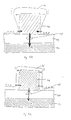
- a common configuration requires deposition of oxide material over a series of metal lines such as shown in Fig. 1(a).
- metal lines 206 extend in the direction perpendicular to the figure.
- Each metal line 206 is electrically connected to a gate 208 at a lower level, which is separated from the substrate 202 by a gate oxide 204.
- Fig. 1(b) shows a highly nonconformal deposition of film 210 over the series of metal lines 206.
- Such a growth pattern may be termed "neutral-flux-limited oxide growth" and results when the thickness of film 210 increases proportionally to the flux of neutral precursors arriving at a surface segment of the metal-line pattern.
- the deposited layer 210 is thicker on top of the metal lines 206 than at the bottom of the gaps between them or at the sidewalls. This is a consequence of geometric shadowing of the isotropic neutral precursors by the topography.
- the second extreme condition is illustrated in Fig.
- the metal lines 206 acquire a charge even if initially neutral. Such charging results from a combination of tunneling currents that are generated through the oxide layer at the top and sidewalls, surface currents that are generated along the sidewall and bottom surface, and electron tunneling through the gate oxide from the substrate.
- Figs. 1(d) and 1(e) illustrate the currents that are generated during deposition of the oxide layer for neutral-flux-limited growth and reaction-rate-limited growth respectively.
- the directionality difference between ions and electrons as they cross the forming layer results in a differential charging pattern so that in addition to acquiring a charge, the metal line is subjected to potential gradients.
- electron shading leads to the accumulation of negative charge at the upper sidewalls of the forming layer, while directional ions positively charge the forming surface in the gaps.
- the combination of a negative potential at the upper sidewall with a positive potential at the gap bottom preferentially deflects less energetic ions towards the sidewall, causing the lower part of the sidewall also to acquire a positive charge.
- Surface currents ensure that no surface potential gradients larger than a threshold value exist, but large electric fields are generated in the oxide layer, particularly near the top and bottom of the sidewalls where surface potentials approach extreme values.
- the oxide field also depends on the metal line potential and the thickness of the oxide layer at each point. It is this thickness dependence that causes deposition of a nonconformal oxide to result in greater metal-line charging and increased gate oxide damage, as shown in Fig. 1(d).
- positive tunneling currents are illustrated with arrows, the thickness of the arrow being roughly proportional to the size of the current.
- a large positive current flows to the metal line 206 through the sidewall bottom region where the oxide is thinnest.
- this current is compensated mostly by electron tunneling from the upper sidewall region, with the current through the gate oxide being comparatively smaller.
- the oxide thickness at the upper sidewalls increases, there is a corresponding decrease in the electron tunneling current there, forcing the current through the gate oxide to increase to compensate for the excess current flow through the sidewall bottom.
- Such charging damage is known to be greater for etching higher aspect-ratio structures, where the aspect ratio is the ratio of the height of a gap to its width, and is expected also to be greater for deposition processes on structures with higher aspect ratios. Since efforts are continually being made simultaneously to decrease the critical structural dimensions and to increase the aspect-ratio capacity of such processes as part of the ongoing quest to pack logic devices more densely, it is desirable to have a process by which the charging damage can reduced.
- a method for depositing a thin film on a substrate in a process chamber comprises flowing a process gas containing a plurality of precursor gases suitable for forming a plasma into the process chamber, and generating a plasma from the process gas to deposit the thin film on the substrate.
- the precursor gases are flowed into the process chamber such that the thin film is deposited at the center of the substrate more rapidly than at an edge of the substrate.
- the process chamber includes a top gas source and a side gas source. At least one of the precursor gases is flowed through the top gas source at a higher rate than through the side gas source. In one such embodiment, every precursor gas is flowed through the top gas source at a higher rate than through the side gas source, and in another such embodiment, every precursor gas is flowed only through the top gas source.
- the methods of the present invention may be embodied in a computer-readable storage medium having a computer-readable program embodied therein for directing operation of a substrate processing system.
- a system may include a process chamber, a plasma generation system, a substrate holder, a gas delivery system, and a system controller.
- the computer-readable program includes instructions for operating the substrate processing system to form a thin film on a substrate disposed in the processing chamber in accordance with the embodiments described above.
- Fabrication of integrated circuits is typically performed on a circular wafer made of a semiconductor such as silicon.
- a plurality of rectilinear devices is formed on the wafer as a rectangular array, leaving four similarly shaped circular segments that remain unprocessed.
- Embodiments of the invention are directed to reducing the possibility of plasma charge damage to such circuits by using a plasma deposition process that begins covering the center of the wafer and works the deposition outwards towards the wafer's edge. The presence of the initial dielectric film at the wafer center prevents destructive charging.
- the technique is adapted for etching processes in addition to deposition processes.
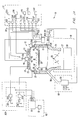
- Fig. 2A illustrates one embodiment of a high density plasma chemical vapor deposition (HDP-CVD) system 10 in which a dielectric layer according to the present invention can be deposited.
- System 10 includes a chamber 13, a vacuum system 70, a source plasma system 80A, a bias plasma system 80B, a gas delivery system 33, and a remote plasma cleaning system 50.
- HDP-CVD high density plasma chemical vapor deposition
- the upper portion of chamber 13 includes a dome 14, which is made of a ceramic dielectric material, such as aluminum oxide or aluminum nitride. Dome 14 defines an upper boundary of a plasma processing region 16. Plasma processing region 16 is bounded on the bottom by the upper surface of a substrate 17 and a substrate support member 18.
- a heater plate 23 and a cold plate 24 surmount, and are thermally coupled to, dome 14.
- Heater plate 23 and cold plate 24 allow control of the dome temperature to within about ⁇ 10 °C over a range of about 100 °C to 200 °C. This allows optimizing the dome temperature for the various processes. For example, it may be desirable to maintain the dome at a higher temperature for cleaning or etching processes than for deposition processes. Accurate control of the dome temperature also reduces the flake or particle counts in the chamber and improves adhesion between the deposited layer and the substrate.
- the lower portion of chamber 13 includes a body member 22, which joins the chamber to the vacuum system.
- a base portion 21 of substrate support member 18 is mounted on, and forms a continuous inner surface with, body member 22.
- Substrates are transferred into and out of chamber 13 by a robot blade (not shown) through an insertion/removal opening (not shown) in the side of chamber 13.
- Lift pins (not shown) are raised and then lowered under the control of a motor (also not shown) to move the substrate from the robot blade at an upper loading position 57 to a lower processing position 56 in which the substrate is placed on a substrate receiving portion 19 of substrate support member 18.
- Substrate receiving portion 19 includes an electrostatic chuck 20 that secures the substrate to substrate support member 18 during substrate processing.
- substrate support member 18 is made from an aluminum oxide or aluminum ceramic material.
- Vacuum system 70 includes throttle body 25, which houses twin-blade throttle valve 26 and is attached to gate valve 27 and turbo-molecular pump 28. It should be noted that throttle body 25 offers minimum obstruction to gas flow, and allows symmetric pumping. Gate valve 27 can isolate pump 28 from throttle body 25, and can also control chamber pressure by restricting the exhaust flow capacity when throttle valve 26 is fully open. The arrangement of the throttle valve, gate valve, and turbo-molecular pump allow accurate and stable control of chamber pressures from between about 1 millitorr to about 2 torr.
- the source plasma system 80A includes a top coil 29 and side coil 30, mounted on dome 14.
- a symmetrical ground shield (not shown) reduces electrical coupling between the coils.
- Top coil 29 is powered by top source RF (SRF) generator 32A
- side coil 30 is powered by side SRF generator 32B, allowing independent power levels and frequencies of operation for each coil.
- SRF source RF
- This dual coil system allows control of the radial ion density in chamber 13, thereby improving plasma uniformity.
- Side coil 30 and top coil 29 are typically inductively driven, which does not require a complimentary electrode.
- the top source RF generator 32A provides up to 2,500 watts of RF power at nominally 2 MHz and the side source RF generator 32B provides up to 5,000 watts of RF power at nominally 2 MHz.
- the operating frequencies of the top and side RF generators may be offset from the nominal operating frequency (e.g. to 1.7-1.9 MHz and 1.9-2.1 MHz, respectively) to improve plasma-generation efficiency.
- a bias plasma system 80B includes a bias RF (“BRF") generator 32C and a bias matching network 32C.
- the bias plasma system 80B capacitively couples substrate portion 17 to body member 22, which act as complimentary electrodes.
- the bias plasma system 80B serves to enhance the transport of plasma species (e.g., ions) created by the source plasma system 80A to the surface of the substrate.
- bias RF generator provides up to 5,000 watts of RF power at 13.56 MHz.
- RF generators 32A and 32B include digitally controlled synthesizers and operate over a frequency range between about 1.8 to about 2.1 MHz. Each generator includes an RF control circuit (not shown) that measures reflected power from the chamber and coil back to the generator and adjusts the frequency of operation to obtain the lowest reflected power, as understood by a person of ordinary skill in the art. RF generators are typically designed to operate into a load with a characteristic impedance of 50 ohms. RF power may be reflected from loads that have a different characteristic impedance than the generator. This can reduce power transferred to the load. Additionally, power reflected from the load back to the generator may overload and damage the generator.
- the impedance of a plasma may range from less than 5 ohms to over 900 ohms, depending on the plasma ion density, among other factors, and because reflected power may be a function of frequency, adjusting the generator frequency according to the reflected power increases the power transferred from the RF generator to the plasma and protects the generator. Another way to reduce reflected power and improve efficiency is with a matching network.
- Matching networks 32A and 32B match the output impedance of generators 32A and 32B with their respective coils 29 and 30.
- the RF control circuit may tune both matching networks by changing the value of capacitors within the matching networks to match the generator to the load as the load changes.
- the RF control circuit may tune a matching network when the power reflected from the load back to the generator exceeds a certain limit.
- One way to provide a constant match, and effectively disable the RF control circuit from tuning the matching network is to set the reflected power limit above any expected value of reflected power. This may help stabilize a plasma under some conditions by holding the matching network constant at its most recent condition.
- the RF control circuit can be used to determine the power delivered to the load (plasma) and may increase or decrease the generator output power to keep the delivered power substantially constant during deposition of a layer.
- a gas delivery system 33 provides gases from several sources, 34A-34F chamber for processing the substrate via gas delivery lines 38 (only some of which are shown).
- gas delivery lines 38 only some of which are shown.
- the actual sources used for sources 34A-34F and the actual connection of delivery lines 38 to chamber 13 varies depending on the deposition and cleaning processes executed within chamber 13. Gases are introduced into chamber 13 through a gas ring 37 and/or a top nozzle 45.
- Fig. 2B is a simplified, partial cross-sectional view of chamber 13 showing additional details of gas ring 37.
- first and second gas sources, 34A and 34B, and first and second gas flow controllers, 35A' and 35B' provide gas to ring plenum 36 in gas ring 37 via gas delivery lines 38 (only some of which are shown).
- Gas ring 37 has a plurality of source gas nozzles 39 (only one of which is shown for purposes of illustration) that provide a uniform flow of gas over the substrate. Nozzle length and nozzle angle may be changed to allow tailoring of the uniformity profile and gas utilization efficiency for a particular process within an individual chamber.
- gas ring 37 has 12 source gas nozzles made from an aluminum oxide ceramic.
- Gas ring 37 also has a plurality of oxidizer gas nozzles 40 (only one of which is shown), which in a preferred embodiment are co-planar with and shorter than source gas nozzles 39, and in one embodiment receive gas from body plenum 41. In some embodiments it is desirable not to mix source gases and oxidizer gases before injecting the gases into chamber 13. In other embodiments, oxidizer gas and source gas may be mixed prior to injecting the gases into chamber 13 by providing apertures (not shown) between body plenum 41 and gas ring plenum 36. In one embodiment, third and fourth gas sources, 34C and 34D, and third and fourth gas flow controllers, 35C and 35D', provide gas to body plenum via gas delivery lines 38.
- the nitrogen source 34F provides nitrogen gas (N 2 ) to the oxidizer nozzles of the gas ring to the chamber for process steps utilizing nitrogen plasma.
- the nitrogen gas could be delivered to the chamber through other or additional inlets, such as the top nozzle.
- Additional valves, such as 43B (other valves not shown), may shut off gas from the flow controllers to the chamber.
- a 3-way valve such as valve 43B, to isolate chamber 13 from delivery line 38A and to vent delivery line 38A to vacuum foreline 44, for example.
- other similar valves such as 43A and 43C, may be incorporated on other gas delivery lines.
- Such 3-way valves may be placed as close to chamber 13 as practical, to minimize the volume of the unvented gas delivery line (between the 3-way valve and the chamber).
- two-way (on-off) valves may be placed between a mass flow controller (“MFC”) and the chamber or between a gas source and an MFC.
- MFC mass flow controller
- chamber 13 also has top nozzle 45 and top vent 46.
- Top nozzle 45 and top vent 46 allow independent control of top and side flows of the gases, which improves film uniformity and allows fine adjustment of the film's deposition and doping parameters.
- Top vent 46 is an annular opening around top nozzle 45.
- first gas source 34A supplies source gas nozzles 39 and top nozzle 45.
- Source nozzle MFC 35A' controls the amount of gas delivered to source gas nozzles 39 and top nozzle MFC 35A controls the amount of gas delivered to top gas nozzle 45.
- two MFCs 35B and 35B' may be used to control the flow of oxygen to both top vent 46 and oxidizer gas nozzles 40 from a single source of oxygen, such as source 34B.
- the gases supplied to top nozzle 45 and top vent 46 may be kept separate prior to flowing the gases into chamber 13, or the gases may be mixed in top plenum 48 before they flow into chamber 13. Separate sources of the same gas may be used to supply various portions of the chamber.
- a remote microwave-generated plasma cleaning system 50 is provided to periodically clean deposition residues from chamber components.
- the cleaning system includes a remote microwave generator 51 that creates a plasma from a cleaning gas source 34E (e.g., molecular fluorine, nitrogen trifluoride, other fluorocarbons or equivalents) in reactor cavity 53.
- a cleaning gas source 34E e.g., molecular fluorine, nitrogen trifluoride, other fluorocarbons or equivalents
- the reactive species resulting from this plasma are conveyed to chamber 13 through cleaning gas feed port 54 via applicator tube 55.
- the materials used to contain the cleaning plasma e.g., cavity 53 and applicator tube 55
- the distance between reactor cavity 53 and feed port 54 should be kept as short as practical, since the concentration of desirable plasma species may decline with distance from reactor cavity 53.
- Generating the cleaning plasma in a remote cavity allows the use of an efficient microwave generator and does not subject chamber components to the temperature, radiation, or bombardment of the glow discharge that may be present in a plasma formed in situ. Consequently, relatively sensitive components, such as electrostatic chuck 20, do not need to be covered with a dummy wafer or otherwise protected, as may be required with an in situ plasma cleaning process.
- System controller 60 controls the operation of system 10.
- controller 60 includes a memory 62, such as a hard disk drive, a floppy disk drive (not shown), and a card rack (not shown) coupled to a processor 61.
- the card rack may contain a single-board computer (SBC) (not shown), analog and digital input/output boards (not shown), interface boards (not shown), and stepper motor controller boards (not shown).
- SBC single-board computer
- the system controller conforms to the Versa Modular European (“VME”) standard, which defines board, card cage, and connector dimensions and types.
- the VME standard also defines the bus structure as having a 16-bit data bus and 24-bit address bus.
- System controller 31 operates under the control of a computer program stored on the hard disk drive or through other computer programs, such as programs stored on a removable disk.
- the computer program dictates, for example, the timing, mixture of gases, RF power levels and other parameters of a particular process.
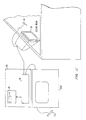
- the interface between a user and the system controller is via a monitor, such as a cathode ray tube ("CRT") 65, and a light pen 66, as depicted in Fig. 2C.
- CTR cathode ray tube
- Fig. 2C is an illustration of a portion of an exemplary system user interface used in conjunction with the exemplary CVD processing chamber of Fig. 2A.
- System controller 60 includes a processor 61 coupled to a computer-readable memory 62.
- memory 62 may be a hard disk drive, but memory 62 may be other kinds of memory, such as ROM, PROM, and others.
- System controller 60 operates under the control of a computer program 63 stored in a computer-readable format within memory 62.
- the computer program dictates the timing, temperatures, gas flows, RF power levels and other parameters of a particular process.
- the interface between a user and the system controller is via a CRT monitor 65 and a light pen 66, as depicted in Fig. 2C.
- two monitors, 65 and 65A, and two light pens, 66 and 66A are used, one mounted in the clean room wall (65) for the operators and the other behind the wall (65A) for the service technicians. Both monitors simultaneously display the same information, but only one light pen (e.g. 66) is enabled.
- the operator touches an area of the display screen and pushes a button (not shown) on the pen. The touched area confirms being selected by the light pen by changing its color or displaying a new menu, for example.
- the computer program code can be written in any conventional computer-readable programming language such as 68000 assembly language, C, C++, or Pascal. Suitable program code is entered into a single file, or multiple files, using a conventional text editor and is stored or embodied in a computer-usable medium, such as a memory system of the computer. If the entered code text is in a high level language, the code is compiled, and the resultant compiler code is then linked with an object code of precompiled windows library routines. To execute the linked compiled object code, the system user invokes the object code causing the computer system to load the code in memory. The CPU reads the code from memory and executes the code to perform the tasks identified in the program.
- a computer-readable programming language such as 68000 assembly language, C, C++, or Pascal.
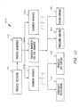
- Fig. 2D shows an illustrative block diagram of the hierarchical control structure of computer program 100.
- a user enters a process set number and process chamber number into a process selector subroutine 110 in response to menus or screens displayed on the CRT monitor by using the light pen interface.
- the process sets are predetermined sets of process parameters necessary to carry out specified processes, and are identified by predefined set numbers.
- Process selector subroutine 110 identifies (i) the desired process chamber in a multichamber system, and (ii) the desired set of process parameters needed to operate the process chamber for performing the desired process.
- the process parameters for performing a specific process relate to conditions such as process gas composition and flow rates, temperature, pressure, plasma conditions such as RF power levels, and chamber dome temperature, and are provided to the user in the form of a recipe.
- the parameters specified by the recipe are entered utilizing the light pen/CRT monitor interface.
- the signals for monitoring the process are provided by the analog and digital input boards of system controller 60, and the signals for controlling the process are output on the analog and digital output boards of system controller 60.
- a process sequencer subroutine 120 comprises program code for accepting the identified process chamber and set of process parameters from the process selector subroutine 110 and for controlling operation of the various process chambers. Multiple users can enter process set numbers and process chamber numbers, or a single user can enter multiple process set numbers and process chamber numbers; sequencer subroutine 120 schedules the selected processes in the desired sequence.
- sequencer subroutine 120 includes a program code to perform the steps of (i) monitoring the operation of the process chambers to determine if the chambers are being used, (ii) determining what processes are being carried out in the chambers being used, and (iii) executing the desired process based on availability of a process chamber and type of process to be carried out.
- sequencer subroutine 120 can be designed to take into consideration the "age" of each particular user-entered request, or the present condition of the process chamber being used in comparison with the desired process conditions for a selected process, or any other relevant factor a system programmer desires to include for determining scheduling priorities.
- sequencer subroutine 120 determines which process chamber and process set combination is going to be executed next, sequencer subroutine 120 initiates execution of the process set by passing the particular process set parameters to a chamber manager subroutine 130A-C, which controls multiple processing tasks in chamber 13 and possibly other chambers (not shown) according to the process set sent by sequencer subroutine 120.
- chamber component subroutines are substrate positioning subroutine 340, process gas control subroutine 150, pressure control subroutine 160, and plasma control subroutine 170.
- chamber manager subroutine 130A selectively schedules or calls the process component subroutines in accordance with the particular process set being executed.
- Chamber manager subroutine 130A schedules process component subroutines in the same manner that sequencer subroutine 120 schedules the process chamber and process set to execute.
- chamber manager subroutine 130A includes steps of monitoring the various chamber components, determining which components need to be operated based on the process parameters for the process set to be executed, and causing execution of a chamber component subroutine responsive to the monitoring and determining steps.
- Substrate positioning subroutine 140 comprises program code for controlling chamber components that are used to load a substrate onto substrate support number 18. Substrate positioning subroutine 140 may also control transfer of a substrate into chamber 13 from, e.g., a plasma-enhanced CVD ("PECVD") reactor or other reactor in the multi-chamber system, after other processing has been completed.
- PECVD plasma-enhanced CVD
- Process gas control subroutine 150 has program code for controlling process gas composition and flow rates. Subroutine 150 controls the open/close position of the safety shut-off valves and also ramps up/ramps down the mass flow controllers to obtain the desired gas flow rates. All chamber component subroutines, including process gas control subroutine 150, are invoked by chamber manager subroutine 130A. Subroutine 150 receives process parameters from chamber manager subroutine 130A related to the desired gas flow rates.
- process gas control subroutine 150 opens the gas supply lines, and repeatedly (i) reads the necessary mass flow controllers, (ii) compares the readings to the desired flow rates received from chamber manager subroutine 130A, and (iii) adjusts the flow rates of the gas supply lines as necessary. Furthermore, process gas control subroutine 150 may include steps for monitoring the gas flow rates for unsafe rates and for activating the safety shut-off valves when an unsafe condition is detected.
- an inert gas such as argon
- the process gas control subroutine 150 is programmed to include steps for flowing the inert gas into chamber 13 for an amount of time necessary to stabilize the pressure in the chamber. The steps described above may then be carried out.
- the process gas control subroutine 150 may include steps for bubbling a delivery gas such as helium through the liquid precursor in a bubbler assembly or for introducing the helium to a liquid injection valve.
- a delivery gas such as helium
- the process gas control subroutine 150 regulates the flow of the delivery gas, the pressure in the bubbler, and the bubbler temperature to obtain the desired process gas flow rates.
- the desired process gas flow rates are transferred to process gas control subroutine 150 as process parameters.
- the process gas control subroutine 150 includes steps for obtaining the necessary delivery gas flow rate, bubbler pressure, and bubbler temperature for the desired process gas flow rate by accessing a stored table containing the necessary values for a given process gas flow rate. Once the necessary values are obtained, the delivery gas flow rate, bubbler pressure and bubbler temperature are monitored, compared to the necessary values and adjusted accordingly.
- the process gas control subroutine 150 may also control the flow of heat-transfer gas, such as helium (He), through the inner and outer passages in the wafer chuck with an independent helium control (IHC) subroutine (not shown).
- the gas flow thermally couples the substrate to the chuck.
- the wafer is heated by the plasma and the chemical reactions that form the layer, and the He cools the substrate through the chuck, which may be water-cooled. This keeps the substrate below a temperature that may damage preexisting features on the substrate.
- Pressure control subroutine 160 includes program code for controlling the pressure in chamber 13 by regulating the size of the opening of throttle valve 26 in the exhaust portion of the chamber.
- the first method relies on characterizing the chamber pressure as it relates to, among other things, the total process gas flow, the size of the process chamber, and the pumping capacity.
- the first method sets throttle valve 26 to a fixed position. Setting throttle valve 26 to a fixed position may eventually result in a steady-state pressure.
- the chamber pressure may be measured, with a manometer for example, and the position of throttle valve 26 may be adjusted according to pressure control subroutine 360, assuming the control point is within the boundaries set by gas flows and exhaust capacity.
- the former method may result in quicker chamber pressure changes, as the measurements, comparisons, and calculations associated with the latter method are not invoked.
- the former method may be desirable where precise control of the chamber pressure is not required, whereas the latter method may be desirable where an accurate, repeatable, and stable pressure is desired, such as during the deposition of a layer.
- pressure control subroutine 160 When pressure control subroutine 160 is invoked, the desired, or target, pressure level is received as a parameter from chamber manager subroutine 130A. Pressure control subroutine 160 measures the pressure in chamber 13 by reading one or more conventional pressure manometers connected to the chamber; compares the measured value(s) to the target pressure; obtains proportional, integral, and differential (PID) values from a stored pressure table corresponding to the target pressure, and adjusts throttle valve 26 according to the PID values obtained from the pressure table. Alternatively, pressure control subroutine 160 may open or close throttle valve 26 to a particular opening size to regulate the pressure in chamber 13 to a desired pressure or pressure range.
- PID proportional, integral, and differential
- Plasma control subroutine 170 comprises program code for controlling the frequency and power output setting of RF generators 32A and 32B and for tuning matching networks 32A and 32B.
- Plasma control subroutine 370 like the previously described chamber component subroutines, is invoked by chamber manager subroutine 330A.
- Fig. 2E shows schematically how various different configurations for the processing system may be used in accordance with the invention.
- the left column of the figure shows a side view of the system while the right column shows a top view.
- the structure of the system shown in detail in Fig. 2A corresponds to part (1) of Fig. 2E.
- the chamber 13 includes a substrate receiving portion 19 with gas sources configured so that there are source gas nozzles 39 configured to act as side gas sources and a top nozzle 45 configured to act as a top gas source.
- top gas source refers to any gas source configured to provide a supply of gas above the substrate receiving portion
- side gas source refers to any gas source configured to provide a supply of gas at the periphery of the substrate receiving portion.
- source gas nozzles 39' within the chamber 13' act as side gas sources because they are configured to provide a supply of gas at the periphery of the substrate receiving portion 19'.
- nozzles 45' act as top gas sources because they provide a supply of gas above the substrate receiving portion 19'. There is no requirement that a top gas source be configured so that the gas supply enter directly from the top of the chamber.
- FIG. 3E Another alternative configuration is shown in part (3) of Fig. 2E, in which the components are denoted with double primes.
- the side gas sources are provided as nozzles 39" that are shorter and lower in the chamber to provide a supply of gas at the periphery of the substrate receiving portion 19".
- the top gas sources are provided as parallel nozzles 45" that are longer and higher in the chamber to provide a supply of gas above the substrate receiving portion 19".
- intermediate nozzles are also provided between the top and side gas sources and may be used to affect the relative flow of gases above and towards the periphery the substrate receiving portion 19".
- Fig. 3 illustrates a simplified cross-sectional view of an integrated circuit 500, which may be made in accordance with use of the present invention.
- integrated circuit 500 includes NMOS and PMOS transistors 503 and 506, which are separated and electrically isolated from each other by a field oxide region 520 formed by local oxidation of silicon ("LOCOS"), or other technique.
- transistors 503 and 506 may be separated and electrically isolated from each other by a groove trench isolation (not shown) when transistors 503 and 506 are both NMOS or both PMOS.
- Each transistor 503 and 506 comprises a source region 512, a drain region 515 and a gate region 518.
- a premetal dielectric (PMD) layer 521 separates transistors 503 and 506 from metal layer 540 with connections between metal layer 540 and the transistors made by contacts 524.
- Metal layer 540 is one of four metal layers, 540, 542, 544, and 546, included in integrated circuit 500. Each metal layer 540, 542, 544, and 546 is separated from adjacent metal layers by respective intermetal dielectric (IMD) layers 527, 528, or 529. Any or all of IMD layers 527, 528, or 529 can be deposited in accordance with embodiments of the present invention. Adjacent metal layers are connected at selected openings by vias 526. Deposited over metal layer 546 are planarized passivation layers 530.
- simplified integrated circuit 500 is for illustrative purposes only.
- One of ordinary skill in the art could implement use of the present invention in relation to fabrication of other integrated circuits such as microprocessors, application specific integrated circuits (ASICs), memory devices, and the like.
- the present invention may be applied to PMOS, NMOS, CMOS, bipolar, or BiCMOS devices.
- the incidence of plasma charge damage was compared for HDP-CVD deposition of undoped silicate glass (USG) using recipes designed to compare center-fast deposition with edge-fast deposition.
- the recipes thus include providing SiH 4 and O 2 to the deposition chamber as precursor gases together with Ar to stabilize the pressure.
- other precursor gases may be used as a source of silicon, such as tetraethylorthosilane (TEOS) or SiF 4 .
- TEOS tetraethylorthosilane
- SiF 4 tetraethylorthosilane
- the center-fast deposition method may be used to reduce plasma charge damage when depositing other oxides, including fluorinated silicate glass (FSG), by an appropriate selection of precursor gases.
- Langmuir probes are commonly used for diagnostic studies of plasmas.
- a schematic of the Langmuir probe setup is shown in Fig. 4.
- the Langmuir probe 302 consists of a tungsten wire 304 within a ceramic sheath 306, which is covered by a grounded aluminum tube 308.
- the probe 302 is inserted into the process chamber 13 to collect measurements, which are transmitted to a plotter 310 over a shielded cable 312.
- Particular adaptations are needed for use of the Langmuir probe 302 in the deposition environments provided by HDP-CVD chambers because the accumulation of oxide on the tip of the plasma probe 302 causes the formation of a time-dependent capacitive voltage divider that decreases the strength of the probe signal.
- the wires were cleaned after each deposition by applying a negative bias to the tip in an argon plasma until the ion current thus collected saturated with time. Measurements were then taken by moving the probe 302 to the appropriate position (e.g. the center or edge of the wafer) and the procedure repeated so that measurements were taken consistently with a clean probe.
- the third and fourth rows respectively specify the source and bias RF power in kW; no bias power is applied in either of these exemplary recipes.
- the remaining rows specify the flow rate of the gases to the process chamber 13 in sccm.
- Argon is first introduced to the process chamber 13, followed by molecular oxygen, and finally followed by silane.
- the edge-fast and center-fast recipes are identical except that in the center-fast recipe, the oxygen and silane flow rates are introduced solely from the top and not the sides in step 7.
- Fig. 5(a) shows that the response of the plasma at the wafer center lags that of the plasma at the wafer edge by approximately 0.4 seconds. This behavior is reversed in Fig. 5(b) where the introduction of silane into the chamber first affects the center trace, with the edge trace lagging by approximately 0.6 seconds.
- different process recipes may be used to produce the characteristically distinct "edge-fast" and "center-fast” deposition processes.
- edge-fast deposition the disturbance caused by the arrival of silane travels inwards from the edge of the wafer but travels outwards from the center of the wafer when a center-fast recipe is used.
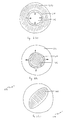
- Fig. 6(a) a schematic representation of edge-fast deposition is depicted. At the specific time illustrated, material has been deposited on the outer region 602 and has not been deposited on the inner region 606. Annular region 604 represents the leading edge of the deposition process over which considerable variation in thickness is expected.
- Fig. 6(b) shows the analogous situation at a specific time for center-fast deposition. In this instance, the inner region 616 is covered with material, the outer region 612 is uncovered, and the intermediate annular region 614 is expected to show large thickness variation as the leading deposition edge.
- the area of the intermediate annular region 604 is a decreasing function of time during edge-fast deposition but the area of the intermediate annular region 614 is an increasing function of time during center-fast deposition.
- the current through each gate structure for devices on the circular wafer tends to increase as a function of time for edge-fast deposition but decreases for center-fast deposition.
- the process of center-fast deposition therefore protects the devices from destructively large currents resulting from the deposition gradients.
- side sources 622 and 624 are used, as exemplified in Fig. 6(c)
- device damage occurs over a roughly elliptical area 626 of the wafer. Since in practice it is impossible to achieve perfectly uniform deposition, the use of center-fast deposition acts to dissipate disturbances arising from the silane-on step over a larger area near the edge of the wafer.
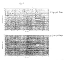
- results of bulk film plasma damage monitoring are shown in Figs. 8(a) and 8(b). While PDM is a blanket film-damage test method that does not measure topography-dependent damage mechanisms, it provides information about high surface charge voltages that would produce high interface surface charges.
- the surface voltage V PDM was measured for the two recipes during the silane-on step, but with a top and side RF power equal to 1.3 kW.
- the'range of V PDM is approximately 0.41 V when the center-fast recipe is used.
- the range is more than twice as large, approximately 0.91 V, when the edge-fast recipe is used, as seen from Fig. 8(b).
- the center-fast recipe thus provides a reduction in surface voltage gradients.
- the higher surface charge voltage produced by the edge-fast recipe indicates that there is more trapped charge near the center of the wafer than when the center-fast recipe is used.
- Figs. 9(a) and 9(b) Time-dependent aspects of the deposition are shown in Figs. 9(a) and 9(b) for the edge-fast and center-fast recipes respectively.
- Optical measurements were taken with an Ocean Optics 1000 spectrometer to determine the time dependence of silane, oxygen, and argon concentrations.
- the intensities of three emission lines for hydrogen (288 nm), oxygen (776 nm), and argon (603 nm) were determined as a function of time, the intensity of the hydrogen line being used as an indicator for the presence of silane.
- the striking of the plasma at time t ⁇ 0, the introduction of O 2 , and the introduction of silane are all readily observed.
- the hydrogen traces allow a comparison of the time taken for hydrogen emission to reach 50% of its final value, which estimates the timescale for diffusion and fragmentation of silane (and the resultant release of hydrogen atoms whose emissions can be detected by the spectrometer). For the edge-fast deposition recipe, this time is approximately 1 s. For the center-fast deposition recipe, the hydrogen trace does not step up until the second silane step when side hydrogen sources are turned on, but reaches 50% of its final value in about half the time. Accordingly, silane is fragmented and diffused more rapidly when the center-fast recipe is used.
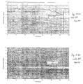
- the plasma probe signals measured at the edge and center of the wafer are shown in Figs. 10(a) and 10(b) for the edge-fast and center-fast recipes respectively.
- the signals are normalized to the level at their respective heat-up steps.
- the signal level subsequent to the period of transition as the new feed gases diffuse into the chamber is a measure of how much oxide has accumulated on the probe tip.
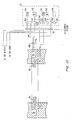
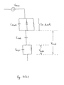
- the dependence of the probe voltage to the voltage at the oxide layer can be understood with the model circuit diagram shown in Fig. 10(c).
- V out V oxide C scope 1 C oxide + 1 C scope -1 , leading to the result that V out decreases as C oxide decreases. [Note that in the C oxide « C scope limit, V out ⁇ V oxide C oxide .]
- the oxide voltage V oxide is itself related to the plasma potential V plasma through the capacitance of the sheath. Thus, the output of the capacitive probe increases as the thickness of the deposited oxide increases.
- Fig. 10(a) indicates that when the edge-fast deposition recipe is used, the oxide forms uniformly at the wafer edge and in the wafer center.
- Fig. 10(b) which shows a faster signal decay at the center, confirms that the deposition of the center-fast recipe is indeed faster at the center.
- center-fast deposition is to supply precursor gases in one recipe step preferentially to top sources. It is also apparent that such center-fast deposition reduces the level of plasma charge damage when compared with otherwise similar edge-fast deposition recipes. Since the reaction design controls current directionality, center-fast processes may also be used in etching processes.
Landscapes
- Chemical & Material Sciences (AREA)
- Engineering & Computer Science (AREA)
- Physics & Mathematics (AREA)
- Plasma & Fusion (AREA)
- General Chemical & Material Sciences (AREA)
- Chemical Kinetics & Catalysis (AREA)
- Materials Engineering (AREA)
- Mechanical Engineering (AREA)
- Metallurgy (AREA)
- Organic Chemistry (AREA)
- Analytical Chemistry (AREA)
- Chemical Vapour Deposition (AREA)
Abstract
Description
| Edge-Fast Recipe | ||||||||
| Step | 1 | 2 | 3 | 4 | 5 | 6 | 7 | 8 |
| Time (s) | 2 | 15 | 2 | 1 | 1 | 20 | 2 | 6 |
| Press | TCL | TCL | TCL | TV100 | TFO | TFO | TFO | TFO |
| SRF (kW) | 0 | 0 | 1.0 | 1.0+2.0 | 1.0+2.0 | 1.3+2.8 | 1.3+3.1 | 1.3+3.1 |
| BRF (kW) | 0 | 0 0 | 0 | 0 | 0 | 0 | 0 | |
| F(Ar) (sccm) | 16+180 | 16+180 | 16+180 | 16+110 | 16+110 | 16+110 | 16+110 | 16+110 |
| F(O2) (sccm) | 0 | 0 | 0 | 0 | 0+30 | 16+110 | 16+110 | 16+110 |
| F(SiH4) | 0 | 0 | 0 | 0 | 0 | 0 | 3+30 | 9+53 |
| Center-Fast Recipe | ||||||||
| Step | 1 | 2 | 3 | 4 | 5 | 6 | 7 | 8 |
| Time (s) | 2 | 15 | 2 | 1 | 1 | 20 | 2 | 6 |
| Press | TCL | TCL | TCL | TV100 | TFO | TFO | TFO | TFO |
| SRF (kW) | 0 | 0 | 1.0 | 1.0+2.0 | 1.0+2.0 | 1.3+2.8 | 1.3+3.1 | 1.3+3.1 |
| BRF (kW) | 0 | 0 | 0 | 0 | 0 | 0 | 0 | 0 |
| F(Ar) (sccm) | 16+180 | 16+180 | 16+180 | 16+110 | 16+110 | 16+110 | 16+110 | 16+110 |
| F(O2) (sccm) | 0 0 0 0 | 0+30 | 16+110 | 0+45 | 16+110 | |||
| F(SiH4) | 0 | 0 | 0 | 0 | 0 | 0 | 0+25 | 9+53 |
Claims (14)
- A method for depositing a film on a substrate in a process chamber, the method comprising:wherein the plurality of precursor gases are flowed into the process chamber such that the thin film is deposited at a center of the substrate more rapidly than at an edge of the substrate.(a) flowing a process gas comprising a plurality of precursor gases suitable for forming a plasma into the process chamber; and(b) generating a plasma from the process gas to deposit the thin film on the substrate,
- A method of depositing a film over a substrate disposed in a chamber of the type having a first set of gas nozzles positioned to provide a flow of gas at a periphery of the substrate and a second nozzle positioned to provide a flow of gas above an upper surface of the substrate, the method comprisingwherein a flow ratio of the process gas provided from the second nozzle relative to the first set of nozzles is greater during the second period than during the first period.(a) flowing a process gas into the chamber through the first set of gas nozzles and through the second nozzle during first and second periods; and(b) forming a plasma from the process gas to deposit a film over the substrate during the first and second periods,
- The method according to claim 1 or 2 wherein the film comprises a silicon oxide and the plurality of precursor gases comprises a silane and a gas that contains oxygen.
- The method according to claim 1 or 2 wherein the process chamber comprises a top gas source and a side gas source and wherein at least one of such precursor gases is flowed through the top gas source at a higher rate than through the side gas source.
- The method according to claim 4 wherein every such precursor gas is flowed through the top gas source at a higher rate than through the side gas source.
- The method according to claim 5 wherein every such precursor gas is flowed only through the top gas source.
- The method according to claim 1 or 2 wherein the process gas further comprises an inert gas, in particular argon.
- The method according to claim 1 or 2 wherein the film comprises a silicon oxide.
- The method according to claim 8 wherein the film is deposited over an intermetal conductive layer.
- The method according to claim 2 wherein the second nozzle comprises a pair of nozzles.
- The method according to claim 10 wherein a silicon-containing gas is provided through one of the pair of nozzles and an oxygen-containing gas is provided through another of the pair of nozzles.
- A method for etching a substrate in a process chamber, the method comprising:wherein the etchant gas is flowed into the process chamber at a higher flow rate above the substrate than at a periphery of the substrate.(a) flowing an etchant gas into the process chamber; and(b) generating a plasma from the etchant gas to etch the substrate,
- A computer-readable storage medium having a computer-readable program embodied therein for directing operation of a substrate processing system including a process chamber; a plasma generation system; a substrate holder; and a gas delivery system configured to introduce gases into the process chamber, the computer-readable program including instructions for operating the substrate processing system to deposit a thin film on a substrate disposed in the process chamber in accordance with any of the preceding claims.
- A substrate processing system comprising:(a) a housing defining a process chamber;(b) a high-density plasma generating system operatively coupled to the process chamber;(c) a substrate holder configured to hold a substrate during substrate processing;(d) a gas-delivery system configured to introduce gases into the process chamber;(e) a pressure-control system for maintaining a selected pressure within the process chamber;(f) a controller for controlling the high-density plasma generating system, the gas-delivery system, and the pressure-control system; and(g) a memory coupled to the controller, the memory comprising a computer-readable medium having a computer-readable program embodied therein for directing operation of the substrate processing system, the computer-readable program including instructions for operating the substrate processing system to deposit a thin film on a substrate disposed in the process chamber in accordance with any of the preceding claims.
Applications Claiming Priority (2)
| Application Number | Priority Date | Filing Date | Title |
|---|---|---|---|
| US09/771,203 US6660662B2 (en) | 2001-01-26 | 2001-01-26 | Method of reducing plasma charge damage for plasma processes |
| US771203 | 2001-01-26 |
Publications (2)
| Publication Number | Publication Date |
|---|---|
| EP1227172A2 true EP1227172A2 (en) | 2002-07-31 |
| EP1227172A3 EP1227172A3 (en) | 2002-11-27 |
Family
ID=25091034
Family Applications (1)
| Application Number | Title | Priority Date | Filing Date |
|---|---|---|---|
| EP01124618A Withdrawn EP1227172A3 (en) | 2001-01-26 | 2001-10-15 | Method of reducing plasma charge damage for plasma processes |
Country Status (5)
| Country | Link |
|---|---|
| US (2) | US6660662B2 (en) |
| EP (1) | EP1227172A3 (en) |
| JP (1) | JP5004396B2 (en) |
| KR (1) | KR100870853B1 (en) |
| TW (1) | TW575893B (en) |
Cited By (1)
| Publication number | Priority date | Publication date | Assignee | Title |
|---|---|---|---|---|
| EP2390898A3 (en) * | 2010-05-26 | 2012-02-01 | Tokyo Electron Limited | Plasma processing apparatus and processing gas supply structure thereof |
Families Citing this family (425)
| Publication number | Priority date | Publication date | Assignee | Title |
|---|---|---|---|---|
| US7144822B1 (en) * | 2002-02-06 | 2006-12-05 | Novellus Systems, Inc. | High density plasma process for optimum film quality and electrical results |
| US20040231798A1 (en) * | 2002-09-13 | 2004-11-25 | Applied Materials, Inc. | Gas delivery system for semiconductor processing |
| KR100517550B1 (en) * | 2002-12-04 | 2005-09-29 | 삼성전자주식회사 | Atomic layer deposition apparatus |
| FR2858333B1 (en) * | 2003-07-31 | 2006-12-08 | Cit Alcatel | METHOD AND DEVICE FOR LOW-AGGRESSIVE DEPOSITION OF PLASMA-ASSISTED VAPOR PHASE DIELECTRIC FILMS |
| US7737382B2 (en) * | 2004-04-01 | 2010-06-15 | Lincoln Global, Inc. | Device for processing welding wire |
| JP2006140492A (en) * | 2004-11-11 | 2006-06-01 | Samsung Electronics Co Ltd | Dry cleaning equipment used in semiconductor device manufacturing |
| KR101232085B1 (en) * | 2006-01-23 | 2013-02-08 | 엘지디스플레이 주식회사 | Cleaning apparatus of Apparatus for Making Thin Film |
| US7790634B2 (en) | 2006-05-30 | 2010-09-07 | Applied Materials, Inc | Method for depositing and curing low-k films for gapfill and conformal film applications |
| US7902080B2 (en) | 2006-05-30 | 2011-03-08 | Applied Materials, Inc. | Deposition-plasma cure cycle process to enhance film quality of silicon dioxide |
| US7825038B2 (en) | 2006-05-30 | 2010-11-02 | Applied Materials, Inc. | Chemical vapor deposition of high quality flow-like silicon dioxide using a silicon containing precursor and atomic oxygen |
| US7498273B2 (en) | 2006-05-30 | 2009-03-03 | Applied Materials, Inc. | Formation of high quality dielectric films of silicon dioxide for STI: usage of different siloxane-based precursors for harp II—remote plasma enhanced deposition processes |
| US20070281106A1 (en) * | 2006-05-30 | 2007-12-06 | Applied Materials, Inc. | Process chamber for dielectric gapfill |
| US8232176B2 (en) | 2006-06-22 | 2012-07-31 | Applied Materials, Inc. | Dielectric deposition and etch back processes for bottom up gapfill |
| US20080095953A1 (en) * | 2006-10-24 | 2008-04-24 | Samsung Electronics Co., Ltd. | Apparatus for depositing thin film and method of depositing the same |
| WO2008154222A1 (en) * | 2007-06-06 | 2008-12-18 | Mks Instruments, Inc. | Particle reduction through gas and plasma source control |
| US7745352B2 (en) | 2007-08-27 | 2010-06-29 | Applied Materials, Inc. | Curing methods for silicon dioxide thin films deposited from alkoxysilane precursor with harp II process |
| KR100916533B1 (en) * | 2007-09-21 | 2009-09-11 | 피에스케이 주식회사 | Substrate Processing Apparatus and Method |
| US7943531B2 (en) | 2007-10-22 | 2011-05-17 | Applied Materials, Inc. | Methods for forming a silicon oxide layer over a substrate |
| US7867923B2 (en) | 2007-10-22 | 2011-01-11 | Applied Materials, Inc. | High quality silicon oxide films by remote plasma CVD from disilane precursors |
| US7803722B2 (en) | 2007-10-22 | 2010-09-28 | Applied Materials, Inc | Methods for forming a dielectric layer within trenches |
| US7541297B2 (en) | 2007-10-22 | 2009-06-02 | Applied Materials, Inc. | Method and system for improving dielectric film quality for void free gap fill |
| US7964040B2 (en) * | 2007-11-08 | 2011-06-21 | Applied Materials, Inc. | Multi-port pumping system for substrate processing chambers |
| US8153348B2 (en) * | 2008-02-20 | 2012-04-10 | Applied Materials, Inc. | Process sequence for formation of patterned hard mask film (RFP) without need for photoresist or dry etch |
| US8357435B2 (en) * | 2008-05-09 | 2013-01-22 | Applied Materials, Inc. | Flowable dielectric equipment and processes |
| US10378106B2 (en) | 2008-11-14 | 2019-08-13 | Asm Ip Holding B.V. | Method of forming insulation film by modified PEALD |
| US9394608B2 (en) | 2009-04-06 | 2016-07-19 | Asm America, Inc. | Semiconductor processing reactor and components thereof |
| US8980382B2 (en) * | 2009-12-02 | 2015-03-17 | Applied Materials, Inc. | Oxygen-doping for non-carbon radical-component CVD films |
| US8741788B2 (en) * | 2009-08-06 | 2014-06-03 | Applied Materials, Inc. | Formation of silicon oxide using non-carbon flowable CVD processes |
| US7935643B2 (en) * | 2009-08-06 | 2011-05-03 | Applied Materials, Inc. | Stress management for tensile films |
| US8802201B2 (en) | 2009-08-14 | 2014-08-12 | Asm America, Inc. | Systems and methods for thin-film deposition of metal oxides using excited nitrogen-oxygen species |
| US7989365B2 (en) * | 2009-08-18 | 2011-08-02 | Applied Materials, Inc. | Remote plasma source seasoning |
| US20110136347A1 (en) * | 2009-10-21 | 2011-06-09 | Applied Materials, Inc. | Point-of-use silylamine generation |
| US8449942B2 (en) * | 2009-11-12 | 2013-05-28 | Applied Materials, Inc. | Methods of curing non-carbon flowable CVD films |
| WO2011090626A2 (en) | 2009-12-30 | 2011-07-28 | Applied Materials, Inc. | Dielectric film growth with radicals produced using flexible nitrogen/hydrogen ratio |
| US8329262B2 (en) * | 2010-01-05 | 2012-12-11 | Applied Materials, Inc. | Dielectric film formation using inert gas excitation |
| SG182336A1 (en) | 2010-01-06 | 2012-08-30 | Applied Materials Inc | Flowable dielectric using oxide liner |
| WO2011084752A2 (en) | 2010-01-07 | 2011-07-14 | Applied Materials, Inc. | In-situ ozone cure for radical-component cvd |
| CN102844848A (en) * | 2010-03-05 | 2012-12-26 | 应用材料公司 | Conformal layers deposited by chemical vapor deposition of radical components |
| US8236708B2 (en) | 2010-03-09 | 2012-08-07 | Applied Materials, Inc. | Reduced pattern loading using bis(diethylamino)silane (C8H22N2Si) as silicon precursor |
| US7994019B1 (en) | 2010-04-01 | 2011-08-09 | Applied Materials, Inc. | Silicon-ozone CVD with reduced pattern loading using incubation period deposition |
| US8476142B2 (en) | 2010-04-12 | 2013-07-02 | Applied Materials, Inc. | Preferential dielectric gapfill |
| US8524004B2 (en) | 2010-06-16 | 2013-09-03 | Applied Materials, Inc. | Loadlock batch ozone cure |
| US8318584B2 (en) | 2010-07-30 | 2012-11-27 | Applied Materials, Inc. | Oxide-rich liner layer for flowable CVD gapfill |
| US9285168B2 (en) | 2010-10-05 | 2016-03-15 | Applied Materials, Inc. | Module for ozone cure and post-cure moisture treatment |
| US8664127B2 (en) | 2010-10-15 | 2014-03-04 | Applied Materials, Inc. | Two silicon-containing precursors for gapfill enhancing dielectric liner |
| US20120180954A1 (en) | 2011-01-18 | 2012-07-19 | Applied Materials, Inc. | Semiconductor processing system and methods using capacitively coupled plasma |
| US10283321B2 (en) | 2011-01-18 | 2019-05-07 | Applied Materials, Inc. | Semiconductor processing system and methods using capacitively coupled plasma |
| US8450191B2 (en) | 2011-01-24 | 2013-05-28 | Applied Materials, Inc. | Polysilicon films by HDP-CVD |
| US8716154B2 (en) | 2011-03-04 | 2014-05-06 | Applied Materials, Inc. | Reduced pattern loading using silicon oxide multi-layers |
| US8445078B2 (en) | 2011-04-20 | 2013-05-21 | Applied Materials, Inc. | Low temperature silicon oxide conversion |
| US8466073B2 (en) | 2011-06-03 | 2013-06-18 | Applied Materials, Inc. | Capping layer for reduced outgassing |
| US9312155B2 (en) | 2011-06-06 | 2016-04-12 | Asm Japan K.K. | High-throughput semiconductor-processing apparatus equipped with multiple dual-chamber modules |
| US10364496B2 (en) | 2011-06-27 | 2019-07-30 | Asm Ip Holding B.V. | Dual section module having shared and unshared mass flow controllers |
| US9404178B2 (en) | 2011-07-15 | 2016-08-02 | Applied Materials, Inc. | Surface treatment and deposition for reduced outgassing |
| US10854498B2 (en) | 2011-07-15 | 2020-12-01 | Asm Ip Holding B.V. | Wafer-supporting device and method for producing same |
| US20130023129A1 (en) | 2011-07-20 | 2013-01-24 | Asm America, Inc. | Pressure transmitter for a semiconductor processing environment |
| US8617989B2 (en) | 2011-09-26 | 2013-12-31 | Applied Materials, Inc. | Liner property improvement |
| US8551891B2 (en) | 2011-10-04 | 2013-10-08 | Applied Materials, Inc. | Remote plasma burn-in |
| US9017481B1 (en) | 2011-10-28 | 2015-04-28 | Asm America, Inc. | Process feed management for semiconductor substrate processing |
| US9659799B2 (en) | 2012-08-28 | 2017-05-23 | Asm Ip Holding B.V. | Systems and methods for dynamic semiconductor process scheduling |
| US8889566B2 (en) | 2012-09-11 | 2014-11-18 | Applied Materials, Inc. | Low cost flowable dielectric films |
| US9021985B2 (en) | 2012-09-12 | 2015-05-05 | Asm Ip Holdings B.V. | Process gas management for an inductively-coupled plasma deposition reactor |
| US10714315B2 (en) | 2012-10-12 | 2020-07-14 | Asm Ip Holdings B.V. | Semiconductor reaction chamber showerhead |
| US9018108B2 (en) | 2013-01-25 | 2015-04-28 | Applied Materials, Inc. | Low shrinkage dielectric films |
| US20160376700A1 (en) | 2013-02-01 | 2016-12-29 | Asm Ip Holding B.V. | System for treatment of deposition reactor |
| US9589770B2 (en) | 2013-03-08 | 2017-03-07 | Asm Ip Holding B.V. | Method and systems for in-situ formation of intermediate reactive species |
| US9484191B2 (en) | 2013-03-08 | 2016-11-01 | Asm Ip Holding B.V. | Pulsed remote plasma method and system |
| US9240412B2 (en) | 2013-09-27 | 2016-01-19 | Asm Ip Holding B.V. | Semiconductor structure and device and methods of forming same using selective epitaxial process |
| JP5917477B2 (en) * | 2013-11-29 | 2016-05-18 | 株式会社日立国際電気 | Substrate processing apparatus, semiconductor device manufacturing method, and program |
| US10683571B2 (en) * | 2014-02-25 | 2020-06-16 | Asm Ip Holding B.V. | Gas supply manifold and method of supplying gases to chamber using same |
| US10167557B2 (en) | 2014-03-18 | 2019-01-01 | Asm Ip Holding B.V. | Gas distribution system, reactor including the system, and methods of using the same |
| US11015245B2 (en) | 2014-03-19 | 2021-05-25 | Asm Ip Holding B.V. | Gas-phase reactor and system having exhaust plenum and components thereof |
| CN105206598B (en) * | 2014-06-26 | 2018-03-30 | 中芯国际集成电路制造(上海)有限公司 | Semiconductor devices and forming method thereof |
| US9412581B2 (en) | 2014-07-16 | 2016-08-09 | Applied Materials, Inc. | Low-K dielectric gapfill by flowable deposition |
| US10858737B2 (en) | 2014-07-28 | 2020-12-08 | Asm Ip Holding B.V. | Showerhead assembly and components thereof |
| US9890456B2 (en) | 2014-08-21 | 2018-02-13 | Asm Ip Holding B.V. | Method and system for in situ formation of gas-phase compounds |
| US10941490B2 (en) | 2014-10-07 | 2021-03-09 | Asm Ip Holding B.V. | Multiple temperature range susceptor, assembly, reactor and system including the susceptor, and methods of using the same |
| US9657845B2 (en) | 2014-10-07 | 2017-05-23 | Asm Ip Holding B.V. | Variable conductance gas distribution apparatus and method |
| KR102263121B1 (en) | 2014-12-22 | 2021-06-09 | 에이에스엠 아이피 홀딩 비.브이. | Semiconductor device and manufacuring method thereof |
| US20160225652A1 (en) | 2015-02-03 | 2016-08-04 | Applied Materials, Inc. | Low temperature chuck for plasma processing systems |
| US10529542B2 (en) | 2015-03-11 | 2020-01-07 | Asm Ip Holdings B.V. | Cross-flow reactor and method |
| US10276355B2 (en) | 2015-03-12 | 2019-04-30 | Asm Ip Holding B.V. | Multi-zone reactor, system including the reactor, and method of using the same |
| US10458018B2 (en) | 2015-06-26 | 2019-10-29 | Asm Ip Holding B.V. | Structures including metal carbide material, devices including the structures, and methods of forming same |
| US10600673B2 (en) | 2015-07-07 | 2020-03-24 | Asm Ip Holding B.V. | Magnetic susceptor to baseplate seal |
| US10083836B2 (en) | 2015-07-24 | 2018-09-25 | Asm Ip Holding B.V. | Formation of boron-doped titanium metal films with high work function |
| US9960072B2 (en) | 2015-09-29 | 2018-05-01 | Asm Ip Holding B.V. | Variable adjustment for precise matching of multiple chamber cavity housings |
| US10211308B2 (en) | 2015-10-21 | 2019-02-19 | Asm Ip Holding B.V. | NbMC layers |
| US10322384B2 (en) | 2015-11-09 | 2019-06-18 | Asm Ip Holding B.V. | Counter flow mixer for process chamber |
| US11139308B2 (en) | 2015-12-29 | 2021-10-05 | Asm Ip Holding B.V. | Atomic layer deposition of III-V compounds to form V-NAND devices |
| US10468251B2 (en) | 2016-02-19 | 2019-11-05 | Asm Ip Holding B.V. | Method for forming spacers using silicon nitride film for spacer-defined multiple patterning |
| US10529554B2 (en) | 2016-02-19 | 2020-01-07 | Asm Ip Holding B.V. | Method for forming silicon nitride film selectively on sidewalls or flat surfaces of trenches |
| US10501866B2 (en) | 2016-03-09 | 2019-12-10 | Asm Ip Holding B.V. | Gas distribution apparatus for improved film uniformity in an epitaxial system |
| US10343920B2 (en) | 2016-03-18 | 2019-07-09 | Asm Ip Holding B.V. | Aligned carbon nanotubes |
| US9892913B2 (en) | 2016-03-24 | 2018-02-13 | Asm Ip Holding B.V. | Radial and thickness control via biased multi-port injection settings |
| US10190213B2 (en) | 2016-04-21 | 2019-01-29 | Asm Ip Holding B.V. | Deposition of metal borides |
| US10865475B2 (en) | 2016-04-21 | 2020-12-15 | Asm Ip Holding B.V. | Deposition of metal borides and silicides |
| US10032628B2 (en) | 2016-05-02 | 2018-07-24 | Asm Ip Holding B.V. | Source/drain performance through conformal solid state doping |
| US10367080B2 (en) | 2016-05-02 | 2019-07-30 | Asm Ip Holding B.V. | Method of forming a germanium oxynitride film |
| KR102592471B1 (en) | 2016-05-17 | 2023-10-20 | 에이에스엠 아이피 홀딩 비.브이. | Method of forming metal interconnection and method of fabricating semiconductor device using the same |
| US11453943B2 (en) | 2016-05-25 | 2022-09-27 | Asm Ip Holding B.V. | Method for forming carbon-containing silicon/metal oxide or nitride film by ALD using silicon precursor and hydrocarbon precursor |
| US10388509B2 (en) | 2016-06-28 | 2019-08-20 | Asm Ip Holding B.V. | Formation of epitaxial layers via dislocation filtering |
| US9859151B1 (en) | 2016-07-08 | 2018-01-02 | Asm Ip Holding B.V. | Selective film deposition method to form air gaps |
| US10612137B2 (en) | 2016-07-08 | 2020-04-07 | Asm Ip Holdings B.V. | Organic reactants for atomic layer deposition |
| US10714385B2 (en) | 2016-07-19 | 2020-07-14 | Asm Ip Holding B.V. | Selective deposition of tungsten |
| KR102354490B1 (en) | 2016-07-27 | 2022-01-21 | 에이에스엠 아이피 홀딩 비.브이. | Method of processing a substrate |
| US9812320B1 (en) | 2016-07-28 | 2017-11-07 | Asm Ip Holding B.V. | Method and apparatus for filling a gap |
| US10395919B2 (en) | 2016-07-28 | 2019-08-27 | Asm Ip Holding B.V. | Method and apparatus for filling a gap |
| KR102532607B1 (en) | 2016-07-28 | 2023-05-15 | 에이에스엠 아이피 홀딩 비.브이. | Substrate processing apparatus and method of operating the same |
| US9887082B1 (en) | 2016-07-28 | 2018-02-06 | Asm Ip Holding B.V. | Method and apparatus for filling a gap |
| KR102613349B1 (en) | 2016-08-25 | 2023-12-14 | 에이에스엠 아이피 홀딩 비.브이. | Exhaust apparatus and substrate processing apparatus and thin film fabricating method using the same |
| US10410943B2 (en) | 2016-10-13 | 2019-09-10 | Asm Ip Holding B.V. | Method for passivating a surface of a semiconductor and related systems |
| US10643826B2 (en) | 2016-10-26 | 2020-05-05 | Asm Ip Holdings B.V. | Methods for thermally calibrating reaction chambers |
| US11532757B2 (en) | 2016-10-27 | 2022-12-20 | Asm Ip Holding B.V. | Deposition of charge trapping layers |
| US10229833B2 (en) | 2016-11-01 | 2019-03-12 | Asm Ip Holding B.V. | Methods for forming a transition metal nitride film on a substrate by atomic layer deposition and related semiconductor device structures |
| US10435790B2 (en) | 2016-11-01 | 2019-10-08 | Asm Ip Holding B.V. | Method of subatmospheric plasma-enhanced ALD using capacitively coupled electrodes with narrow gap |
| US10714350B2 (en) | 2016-11-01 | 2020-07-14 | ASM IP Holdings, B.V. | Methods for forming a transition metal niobium nitride film on a substrate by atomic layer deposition and related semiconductor device structures |
| US10643904B2 (en) | 2016-11-01 | 2020-05-05 | Asm Ip Holdings B.V. | Methods for forming a semiconductor device and related semiconductor device structures |
| US10134757B2 (en) | 2016-11-07 | 2018-11-20 | Asm Ip Holding B.V. | Method of processing a substrate and a device manufactured by using the method |
| KR102546317B1 (en) | 2016-11-15 | 2023-06-21 | 에이에스엠 아이피 홀딩 비.브이. | Gas supply unit and substrate processing apparatus including the same |
| US10340135B2 (en) | 2016-11-28 | 2019-07-02 | Asm Ip Holding B.V. | Method of topologically restricted plasma-enhanced cyclic deposition of silicon or metal nitride |
| JP2018093150A (en) * | 2016-12-07 | 2018-06-14 | 東京エレクトロン株式会社 | Film forming apparatus and film forming method |
| KR102762543B1 (en) | 2016-12-14 | 2025-02-05 | 에이에스엠 아이피 홀딩 비.브이. | Substrate processing apparatus |
| US11447861B2 (en) | 2016-12-15 | 2022-09-20 | Asm Ip Holding B.V. | Sequential infiltration synthesis apparatus and a method of forming a patterned structure |
| US11581186B2 (en) | 2016-12-15 | 2023-02-14 | Asm Ip Holding B.V. | Sequential infiltration synthesis apparatus |
| KR102700194B1 (en) | 2016-12-19 | 2024-08-28 | 에이에스엠 아이피 홀딩 비.브이. | Substrate processing apparatus |
| US10269558B2 (en) | 2016-12-22 | 2019-04-23 | Asm Ip Holding B.V. | Method of forming a structure on a substrate |
| US10867788B2 (en) | 2016-12-28 | 2020-12-15 | Asm Ip Holding B.V. | Method of forming a structure on a substrate |
| US11390950B2 (en) | 2017-01-10 | 2022-07-19 | Asm Ip Holding B.V. | Reactor system and method to reduce residue buildup during a film deposition process |
| US10655221B2 (en) | 2017-02-09 | 2020-05-19 | Asm Ip Holding B.V. | Method for depositing oxide film by thermal ALD and PEALD |
| US10468261B2 (en) | 2017-02-15 | 2019-11-05 | Asm Ip Holding B.V. | Methods for forming a metallic film on a substrate by cyclical deposition and related semiconductor device structures |
| US10529563B2 (en) | 2017-03-29 | 2020-01-07 | Asm Ip Holdings B.V. | Method for forming doped metal oxide films on a substrate by cyclical deposition and related semiconductor device structures |
| US10283353B2 (en) | 2017-03-29 | 2019-05-07 | Asm Ip Holding B.V. | Method of reforming insulating film deposited on substrate with recess pattern |
| KR102457289B1 (en) | 2017-04-25 | 2022-10-21 | 에이에스엠 아이피 홀딩 비.브이. | Method for depositing a thin film and manufacturing a semiconductor device |
| US10892156B2 (en) | 2017-05-08 | 2021-01-12 | Asm Ip Holding B.V. | Methods for forming a silicon nitride film on a substrate and related semiconductor device structures |
| US10446393B2 (en) | 2017-05-08 | 2019-10-15 | Asm Ip Holding B.V. | Methods for forming silicon-containing epitaxial layers and related semiconductor device structures |
| US10770286B2 (en) | 2017-05-08 | 2020-09-08 | Asm Ip Holdings B.V. | Methods for selectively forming a silicon nitride film on a substrate and related semiconductor device structures |
| US10504742B2 (en) | 2017-05-31 | 2019-12-10 | Asm Ip Holding B.V. | Method of atomic layer etching using hydrogen plasma |
| US10886123B2 (en) | 2017-06-02 | 2021-01-05 | Asm Ip Holding B.V. | Methods for forming low temperature semiconductor layers and related semiconductor device structures |
| US12040200B2 (en) | 2017-06-20 | 2024-07-16 | Asm Ip Holding B.V. | Semiconductor processing apparatus and methods for calibrating a semiconductor processing apparatus |
| US11306395B2 (en) | 2017-06-28 | 2022-04-19 | Asm Ip Holding B.V. | Methods for depositing a transition metal nitride film on a substrate by atomic layer deposition and related deposition apparatus |
| US10685834B2 (en) | 2017-07-05 | 2020-06-16 | Asm Ip Holdings B.V. | Methods for forming a silicon germanium tin layer and related semiconductor device structures |
| TWI794238B (en) | 2017-07-13 | 2023-03-01 | 荷蘭商Asm智慧財產控股公司 | Apparatus and method for removal of oxide and carbon from semiconductor films in a single processing chamber |
| KR20190009245A (en) | 2017-07-18 | 2019-01-28 | 에이에스엠 아이피 홀딩 비.브이. | Methods for forming a semiconductor device structure and related semiconductor device structures |
| US11374112B2 (en) | 2017-07-19 | 2022-06-28 | Asm Ip Holding B.V. | Method for depositing a group IV semiconductor and related semiconductor device structures |
| US11018002B2 (en) | 2017-07-19 | 2021-05-25 | Asm Ip Holding B.V. | Method for selectively depositing a Group IV semiconductor and related semiconductor device structures |
| US10541333B2 (en) | 2017-07-19 | 2020-01-21 | Asm Ip Holding B.V. | Method for depositing a group IV semiconductor and related semiconductor device structures |
| US10590535B2 (en) | 2017-07-26 | 2020-03-17 | Asm Ip Holdings B.V. | Chemical treatment, deposition and/or infiltration apparatus and method for using the same |
| US10312055B2 (en) | 2017-07-26 | 2019-06-04 | Asm Ip Holding B.V. | Method of depositing film by PEALD using negative bias |
| US10605530B2 (en) | 2017-07-26 | 2020-03-31 | Asm Ip Holding B.V. | Assembly of a liner and a flange for a vertical furnace as well as the liner and the vertical furnace |
| TWI815813B (en) | 2017-08-04 | 2023-09-21 | 荷蘭商Asm智慧財產控股公司 | Showerhead assembly for distributing a gas within a reaction chamber |
| US10770336B2 (en) | 2017-08-08 | 2020-09-08 | Asm Ip Holding B.V. | Substrate lift mechanism and reactor including same |
| US10692741B2 (en) | 2017-08-08 | 2020-06-23 | Asm Ip Holdings B.V. | Radiation shield |
| US11769682B2 (en) | 2017-08-09 | 2023-09-26 | Asm Ip Holding B.V. | Storage apparatus for storing cassettes for substrates and processing apparatus equipped therewith |
| US10249524B2 (en) | 2017-08-09 | 2019-04-02 | Asm Ip Holding B.V. | Cassette holder assembly for a substrate cassette and holding member for use in such assembly |
| US11139191B2 (en) | 2017-08-09 | 2021-10-05 | Asm Ip Holding B.V. | Storage apparatus for storing cassettes for substrates and processing apparatus equipped therewith |
| US10236177B1 (en) | 2017-08-22 | 2019-03-19 | ASM IP Holding B.V.. | Methods for depositing a doped germanium tin semiconductor and related semiconductor device structures |
| USD900036S1 (en) | 2017-08-24 | 2020-10-27 | Asm Ip Holding B.V. | Heater electrical connector and adapter |
| US11830730B2 (en) | 2017-08-29 | 2023-11-28 | Asm Ip Holding B.V. | Layer forming method and apparatus |
| KR102491945B1 (en) | 2017-08-30 | 2023-01-26 | 에이에스엠 아이피 홀딩 비.브이. | Substrate processing apparatus |
| US11295980B2 (en) | 2017-08-30 | 2022-04-05 | Asm Ip Holding B.V. | Methods for depositing a molybdenum metal film over a dielectric surface of a substrate by a cyclical deposition process and related semiconductor device structures |
| US11056344B2 (en) | 2017-08-30 | 2021-07-06 | Asm Ip Holding B.V. | Layer forming method |
| KR102401446B1 (en) | 2017-08-31 | 2022-05-24 | 에이에스엠 아이피 홀딩 비.브이. | Substrate processing apparatus |
| US10607895B2 (en) | 2017-09-18 | 2020-03-31 | Asm Ip Holdings B.V. | Method for forming a semiconductor device structure comprising a gate fill metal |
| KR102630301B1 (en) | 2017-09-21 | 2024-01-29 | 에이에스엠 아이피 홀딩 비.브이. | Method of sequential infiltration synthesis treatment of infiltrateable material and structures and devices formed using same |
| US10844484B2 (en) | 2017-09-22 | 2020-11-24 | Asm Ip Holding B.V. | Apparatus for dispensing a vapor phase reactant to a reaction chamber and related methods |
| US10658205B2 (en) | 2017-09-28 | 2020-05-19 | Asm Ip Holdings B.V. | Chemical dispensing apparatus and methods for dispensing a chemical to a reaction chamber |
| US10403504B2 (en) | 2017-10-05 | 2019-09-03 | Asm Ip Holding B.V. | Method for selectively depositing a metallic film on a substrate |
| US10319588B2 (en) | 2017-10-10 | 2019-06-11 | Asm Ip Holding B.V. | Method for depositing a metal chalcogenide on a substrate by cyclical deposition |
| US10923344B2 (en) | 2017-10-30 | 2021-02-16 | Asm Ip Holding B.V. | Methods for forming a semiconductor structure and related semiconductor structures |
| KR102443047B1 (en) | 2017-11-16 | 2022-09-14 | 에이에스엠 아이피 홀딩 비.브이. | Substrate processing apparatus method and apparatus manufactured thereby |
| US10910262B2 (en) | 2017-11-16 | 2021-02-02 | Asm Ip Holding B.V. | Method of selectively depositing a capping layer structure on a semiconductor device structure |
| US11022879B2 (en) | 2017-11-24 | 2021-06-01 | Asm Ip Holding B.V. | Method of forming an enhanced unexposed photoresist layer |
| WO2019103613A1 (en) | 2017-11-27 | 2019-05-31 | Asm Ip Holding B.V. | A storage device for storing wafer cassettes for use with a batch furnace |
| TWI791689B (en) | 2017-11-27 | 2023-02-11 | 荷蘭商Asm智慧財產控股私人有限公司 | Apparatus including a clean mini environment |
| US10290508B1 (en) | 2017-12-05 | 2019-05-14 | Asm Ip Holding B.V. | Method for forming vertical spacers for spacer-defined patterning |
| US10872771B2 (en) | 2018-01-16 | 2020-12-22 | Asm Ip Holding B. V. | Method for depositing a material film on a substrate within a reaction chamber by a cyclical deposition process and related device structures |
| US11482412B2 (en) | 2018-01-19 | 2022-10-25 | Asm Ip Holding B.V. | Method for depositing a gap-fill layer by plasma-assisted deposition |
| TWI799494B (en) | 2018-01-19 | 2023-04-21 | 荷蘭商Asm 智慧財產控股公司 | Deposition method |
| USD903477S1 (en) | 2018-01-24 | 2020-12-01 | Asm Ip Holdings B.V. | Metal clamp |
| US11018047B2 (en) | 2018-01-25 | 2021-05-25 | Asm Ip Holding B.V. | Hybrid lift pin |
| US10535516B2 (en) | 2018-02-01 | 2020-01-14 | Asm Ip Holdings B.V. | Method for depositing a semiconductor structure on a surface of a substrate and related semiconductor structures |
| USD880437S1 (en) | 2018-02-01 | 2020-04-07 | Asm Ip Holding B.V. | Gas supply plate for semiconductor manufacturing apparatus |
| US11081345B2 (en) | 2018-02-06 | 2021-08-03 | Asm Ip Holding B.V. | Method of post-deposition treatment for silicon oxide film |
| US10896820B2 (en) | 2018-02-14 | 2021-01-19 | Asm Ip Holding B.V. | Method for depositing a ruthenium-containing film on a substrate by a cyclical deposition process |
| WO2019158960A1 (en) | 2018-02-14 | 2019-08-22 | Asm Ip Holding B.V. | A method for depositing a ruthenium-containing film on a substrate by a cyclical deposition process |
| US10731249B2 (en) | 2018-02-15 | 2020-08-04 | Asm Ip Holding B.V. | Method of forming a transition metal containing film on a substrate by a cyclical deposition process, a method for supplying a transition metal halide compound to a reaction chamber, and related vapor deposition apparatus |
| US10658181B2 (en) | 2018-02-20 | 2020-05-19 | Asm Ip Holding B.V. | Method of spacer-defined direct patterning in semiconductor fabrication |
| KR102636427B1 (en) | 2018-02-20 | 2024-02-13 | 에이에스엠 아이피 홀딩 비.브이. | Substrate processing method and apparatus |
| US10975470B2 (en) | 2018-02-23 | 2021-04-13 | Asm Ip Holding B.V. | Apparatus for detecting or monitoring for a chemical precursor in a high temperature environment |
| US11473195B2 (en) | 2018-03-01 | 2022-10-18 | Asm Ip Holding B.V. | Semiconductor processing apparatus and a method for processing a substrate |
| US11629406B2 (en) | 2018-03-09 | 2023-04-18 | Asm Ip Holding B.V. | Semiconductor processing apparatus comprising one or more pyrometers for measuring a temperature of a substrate during transfer of the substrate |
| US11114283B2 (en) | 2018-03-16 | 2021-09-07 | Asm Ip Holding B.V. | Reactor, system including the reactor, and methods of manufacturing and using same |
| KR102646467B1 (en) | 2018-03-27 | 2024-03-11 | 에이에스엠 아이피 홀딩 비.브이. | Method of forming an electrode on a substrate and a semiconductor device structure including an electrode |
| US11088002B2 (en) | 2018-03-29 | 2021-08-10 | Asm Ip Holding B.V. | Substrate rack and a substrate processing system and method |
| US11230766B2 (en) | 2018-03-29 | 2022-01-25 | Asm Ip Holding B.V. | Substrate processing apparatus and method |
| US10510536B2 (en) | 2018-03-29 | 2019-12-17 | Asm Ip Holding B.V. | Method of depositing a co-doped polysilicon film on a surface of a substrate within a reaction chamber |
| KR102501472B1 (en) | 2018-03-30 | 2023-02-20 | 에이에스엠 아이피 홀딩 비.브이. | Substrate processing method |
| KR102600229B1 (en) | 2018-04-09 | 2023-11-10 | 에이에스엠 아이피 홀딩 비.브이. | Substrate supporting device, substrate processing apparatus including the same and substrate processing method |
| US12025484B2 (en) | 2018-05-08 | 2024-07-02 | Asm Ip Holding B.V. | Thin film forming method |
| TWI843623B (en) | 2018-05-08 | 2024-05-21 | 荷蘭商Asm Ip私人控股有限公司 | Methods for depositing an oxide film on a substrate by a cyclical deposition process and related device structures |
| US12272527B2 (en) | 2018-05-09 | 2025-04-08 | Asm Ip Holding B.V. | Apparatus for use with hydrogen radicals and method of using same |
| KR20190129718A (en) | 2018-05-11 | 2019-11-20 | 에이에스엠 아이피 홀딩 비.브이. | Methods for forming a doped metal carbide film on a substrate and related semiconductor device structures |
| KR102596988B1 (en) | 2018-05-28 | 2023-10-31 | 에이에스엠 아이피 홀딩 비.브이. | Method of processing a substrate and a device manufactured by the same |
| US11718913B2 (en) | 2018-06-04 | 2023-08-08 | Asm Ip Holding B.V. | Gas distribution system and reactor system including same |
| TWI840362B (en) | 2018-06-04 | 2024-05-01 | 荷蘭商Asm Ip私人控股有限公司 | Wafer handling chamber with moisture reduction |
| US11286562B2 (en) | 2018-06-08 | 2022-03-29 | Asm Ip Holding B.V. | Gas-phase chemical reactor and method of using same |
| KR102568797B1 (en) | 2018-06-21 | 2023-08-21 | 에이에스엠 아이피 홀딩 비.브이. | Substrate processing system |
| US10797133B2 (en) | 2018-06-21 | 2020-10-06 | Asm Ip Holding B.V. | Method for depositing a phosphorus doped silicon arsenide film and related semiconductor device structures |
| WO2020003000A1 (en) | 2018-06-27 | 2020-01-02 | Asm Ip Holding B.V. | Cyclic deposition methods for forming metal-containing material and films and structures including the metal-containing material |
| KR20250134000A (en) | 2018-06-27 | 2025-09-09 | 에이에스엠 아이피 홀딩 비.브이. | Cyclic deposition methods for forming metal-containing material and films and structures including the metal-containing material |
| KR102686758B1 (en) | 2018-06-29 | 2024-07-18 | 에이에스엠 아이피 홀딩 비.브이. | Method for depositing a thin film and manufacturing a semiconductor device |
| US10612136B2 (en) | 2018-06-29 | 2020-04-07 | ASM IP Holding, B.V. | Temperature-controlled flange and reactor system including same |
| US10755922B2 (en) | 2018-07-03 | 2020-08-25 | Asm Ip Holding B.V. | Method for depositing silicon-free carbon-containing film as gap-fill layer by pulse plasma-assisted deposition |
| US10388513B1 (en) | 2018-07-03 | 2019-08-20 | Asm Ip Holding B.V. | Method for depositing silicon-free carbon-containing film as gap-fill layer by pulse plasma-assisted deposition |
| US10767789B2 (en) | 2018-07-16 | 2020-09-08 | Asm Ip Holding B.V. | Diaphragm valves, valve components, and methods for forming valve components |
| US10483099B1 (en) | 2018-07-26 | 2019-11-19 | Asm Ip Holding B.V. | Method for forming thermally stable organosilicon polymer film |
| US11053591B2 (en) | 2018-08-06 | 2021-07-06 | Asm Ip Holding B.V. | Multi-port gas injection system and reactor system including same |
| US10883175B2 (en) | 2018-08-09 | 2021-01-05 | Asm Ip Holding B.V. | Vertical furnace for processing substrates and a liner for use therein |
| US10829852B2 (en) | 2018-08-16 | 2020-11-10 | Asm Ip Holding B.V. | Gas distribution device for a wafer processing apparatus |
| US11430674B2 (en) | 2018-08-22 | 2022-08-30 | Asm Ip Holding B.V. | Sensor array, apparatus for dispensing a vapor phase reactant to a reaction chamber and related methods |
| KR102707956B1 (en) | 2018-09-11 | 2024-09-19 | 에이에스엠 아이피 홀딩 비.브이. | Method for deposition of a thin film |
| US11024523B2 (en) | 2018-09-11 | 2021-06-01 | Asm Ip Holding B.V. | Substrate processing apparatus and method |
| US11049751B2 (en) | 2018-09-14 | 2021-06-29 | Asm Ip Holding B.V. | Cassette supply system to store and handle cassettes and processing apparatus equipped therewith |
| CN110970344B (en) | 2018-10-01 | 2024-10-25 | Asmip控股有限公司 | Substrate holding device, system including the same and method of using the same |
| US11232963B2 (en) | 2018-10-03 | 2022-01-25 | Asm Ip Holding B.V. | Substrate processing apparatus and method |
| KR102592699B1 (en) | 2018-10-08 | 2023-10-23 | 에이에스엠 아이피 홀딩 비.브이. | Substrate support unit and apparatuses for depositing thin film and processing the substrate including the same |
| US10847365B2 (en) | 2018-10-11 | 2020-11-24 | Asm Ip Holding B.V. | Method of forming conformal silicon carbide film by cyclic CVD |
| US10811256B2 (en) | 2018-10-16 | 2020-10-20 | Asm Ip Holding B.V. | Method for etching a carbon-containing feature |
| KR102605121B1 (en) | 2018-10-19 | 2023-11-23 | 에이에스엠 아이피 홀딩 비.브이. | Substrate processing apparatus and substrate processing method |
| KR102546322B1 (en) | 2018-10-19 | 2023-06-21 | 에이에스엠 아이피 홀딩 비.브이. | Substrate processing apparatus and substrate processing method |
| USD948463S1 (en) | 2018-10-24 | 2022-04-12 | Asm Ip Holding B.V. | Susceptor for semiconductor substrate supporting apparatus |
| US10381219B1 (en) | 2018-10-25 | 2019-08-13 | Asm Ip Holding B.V. | Methods for forming a silicon nitride film |
| US12378665B2 (en) | 2018-10-26 | 2025-08-05 | Asm Ip Holding B.V. | High temperature coatings for a preclean and etch apparatus and related methods |
| US11087997B2 (en) | 2018-10-31 | 2021-08-10 | Asm Ip Holding B.V. | Substrate processing apparatus for processing substrates |
| KR102748291B1 (en) | 2018-11-02 | 2024-12-31 | 에이에스엠 아이피 홀딩 비.브이. | Substrate support unit and substrate processing apparatus including the same |
| US11572620B2 (en) | 2018-11-06 | 2023-02-07 | Asm Ip Holding B.V. | Methods for selectively depositing an amorphous silicon film on a substrate |
| US11031242B2 (en) | 2018-11-07 | 2021-06-08 | Asm Ip Holding B.V. | Methods for depositing a boron doped silicon germanium film |
| US10847366B2 (en) | 2018-11-16 | 2020-11-24 | Asm Ip Holding B.V. | Methods for depositing a transition metal chalcogenide film on a substrate by a cyclical deposition process |
| US10818758B2 (en) | 2018-11-16 | 2020-10-27 | Asm Ip Holding B.V. | Methods for forming a metal silicate film on a substrate in a reaction chamber and related semiconductor device structures |
| US10559458B1 (en) | 2018-11-26 | 2020-02-11 | Asm Ip Holding B.V. | Method of forming oxynitride film |
| US12040199B2 (en) | 2018-11-28 | 2024-07-16 | Asm Ip Holding B.V. | Substrate processing apparatus for processing substrates |
| US11217444B2 (en) | 2018-11-30 | 2022-01-04 | Asm Ip Holding B.V. | Method for forming an ultraviolet radiation responsive metal oxide-containing film |
| KR102636428B1 (en) | 2018-12-04 | 2024-02-13 | 에이에스엠 아이피 홀딩 비.브이. | A method for cleaning a substrate processing apparatus |
| US11158513B2 (en) | 2018-12-13 | 2021-10-26 | Asm Ip Holding B.V. | Methods for forming a rhenium-containing film on a substrate by a cyclical deposition process and related semiconductor device structures |
| JP7504584B2 (en) | 2018-12-14 | 2024-06-24 | エーエスエム・アイピー・ホールディング・ベー・フェー | Method and system for forming device structures using selective deposition of gallium nitride - Patents.com |
| JP7190894B2 (en) * | 2018-12-21 | 2022-12-16 | 昭和電工株式会社 | SiC chemical vapor deposition equipment |
| TWI866480B (en) | 2019-01-17 | 2024-12-11 | 荷蘭商Asm Ip 私人控股有限公司 | Methods of forming a transition metal containing film on a substrate by a cyclical deposition process |
| KR102727227B1 (en) | 2019-01-22 | 2024-11-07 | 에이에스엠 아이피 홀딩 비.브이. | Semiconductor processing device |
| CN111524788B (en) | 2019-02-01 | 2023-11-24 | Asm Ip私人控股有限公司 | Method for forming topologically selective films of silicon oxide |
| TWI845607B (en) | 2019-02-20 | 2024-06-21 | 荷蘭商Asm Ip私人控股有限公司 | Cyclical deposition method and apparatus for filling a recess formed within a substrate surface |
| KR102626263B1 (en) | 2019-02-20 | 2024-01-16 | 에이에스엠 아이피 홀딩 비.브이. | Cyclical deposition method including treatment step and apparatus for same |
| TWI838458B (en) | 2019-02-20 | 2024-04-11 | 荷蘭商Asm Ip私人控股有限公司 | Apparatus and methods for plug fill deposition in 3-d nand applications |
| KR102638425B1 (en) | 2019-02-20 | 2024-02-21 | 에이에스엠 아이피 홀딩 비.브이. | Method and apparatus for filling a recess formed within a substrate surface |
| TWI842826B (en) | 2019-02-22 | 2024-05-21 | 荷蘭商Asm Ip私人控股有限公司 | Substrate processing apparatus and method for processing substrate |
| KR102858005B1 (en) | 2019-03-08 | 2025-09-09 | 에이에스엠 아이피 홀딩 비.브이. | Method for Selective Deposition of Silicon Nitride Layer and Structure Including Selectively-Deposited Silicon Nitride Layer |
| KR102782593B1 (en) | 2019-03-08 | 2025-03-14 | 에이에스엠 아이피 홀딩 비.브이. | Structure Including SiOC Layer and Method of Forming Same |
| US11742198B2 (en) | 2019-03-08 | 2023-08-29 | Asm Ip Holding B.V. | Structure including SiOCN layer and method of forming same |
| JP2020167398A (en) | 2019-03-28 | 2020-10-08 | エーエスエム・アイピー・ホールディング・ベー・フェー | Door openers and substrate processing equipment provided with door openers |
| KR102809999B1 (en) | 2019-04-01 | 2025-05-19 | 에이에스엠 아이피 홀딩 비.브이. | Method of manufacturing semiconductor device |
| KR102897355B1 (en) | 2019-04-19 | 2025-12-08 | 에이에스엠 아이피 홀딩 비.브이. | Layer forming method and apparatus |
| KR20200125453A (en) | 2019-04-24 | 2020-11-04 | 에이에스엠 아이피 홀딩 비.브이. | Gas-phase reactor system and method of using same |
| KR102869364B1 (en) | 2019-05-07 | 2025-10-10 | 에이에스엠 아이피 홀딩 비.브이. | Method for Reforming Amorphous Carbon Polymer Film |
| KR102929471B1 (en) | 2019-05-07 | 2026-02-20 | 에이에스엠 아이피 홀딩 비.브이. | Chemical source vessel with dip tube |
| KR102929472B1 (en) | 2019-05-10 | 2026-02-20 | 에이에스엠 아이피 홀딩 비.브이. | Method of depositing material onto a surface and structure formed according to the method |
| JP7598201B2 (en) | 2019-05-16 | 2024-12-11 | エーエスエム・アイピー・ホールディング・ベー・フェー | Wafer boat handling apparatus, vertical batch furnace and method |
| JP7612342B2 (en) | 2019-05-16 | 2025-01-14 | エーエスエム・アイピー・ホールディング・ベー・フェー | Wafer boat handling apparatus, vertical batch furnace and method |
| USD975665S1 (en) | 2019-05-17 | 2023-01-17 | Asm Ip Holding B.V. | Susceptor shaft |
| USD947913S1 (en) | 2019-05-17 | 2022-04-05 | Asm Ip Holding B.V. | Susceptor shaft |
| USD935572S1 (en) | 2019-05-24 | 2021-11-09 | Asm Ip Holding B.V. | Gas channel plate |
| USD922229S1 (en) | 2019-06-05 | 2021-06-15 | Asm Ip Holding B.V. | Device for controlling a temperature of a gas supply unit |
| KR20200141003A (en) | 2019-06-06 | 2020-12-17 | 에이에스엠 아이피 홀딩 비.브이. | Gas-phase reactor system including a gas detector |
| KR102918757B1 (en) | 2019-06-10 | 2026-01-28 | 에이에스엠 아이피 홀딩 비.브이. | Method for cleaning quartz epitaxial chambers |
| KR20200143254A (en) | 2019-06-11 | 2020-12-23 | 에이에스엠 아이피 홀딩 비.브이. | Method of forming an electronic structure using an reforming gas, system for performing the method, and structure formed using the method |
| USD944946S1 (en) | 2019-06-14 | 2022-03-01 | Asm Ip Holding B.V. | Shower plate |
| USD931978S1 (en) | 2019-06-27 | 2021-09-28 | Asm Ip Holding B.V. | Showerhead vacuum transport |
| KR102911421B1 (en) | 2019-07-03 | 2026-01-12 | 에이에스엠 아이피 홀딩 비.브이. | Temperature control assembly for substrate processing apparatus and method of using same |
| JP7499079B2 (en) | 2019-07-09 | 2024-06-13 | エーエスエム・アイピー・ホールディング・ベー・フェー | Plasma device using coaxial waveguide and substrate processing method |
| CN112216646B (en) | 2019-07-10 | 2026-02-10 | Asmip私人控股有限公司 | Substrate support assembly and substrate processing apparatus including the thereof |
| KR102895115B1 (en) | 2019-07-16 | 2025-12-03 | 에이에스엠 아이피 홀딩 비.브이. | Substrate processing apparatus |
| KR102860110B1 (en) | 2019-07-17 | 2025-09-16 | 에이에스엠 아이피 홀딩 비.브이. | Methods of forming silicon germanium structures |
| KR102955799B1 (en) | 2019-07-17 | 2026-04-21 | 에이에스엠 아이피 홀딩 비.브이. | Radical assist ignition plasma system and method |
| US11643724B2 (en) | 2019-07-18 | 2023-05-09 | Asm Ip Holding B.V. | Method of forming structures using a neutral beam |
| TWI839544B (en) | 2019-07-19 | 2024-04-21 | 荷蘭商Asm Ip私人控股有限公司 | Method of forming topology-controlled amorphous carbon polymer film |
| KR102903090B1 (en) | 2019-07-19 | 2025-12-19 | 에이에스엠 아이피 홀딩 비.브이. | Method of Forming Topology-Controlled Amorphous Carbon Polymer Film |
| TWI851767B (en) | 2019-07-29 | 2024-08-11 | 荷蘭商Asm Ip私人控股有限公司 | Methods for selective deposition utilizing n-type dopants and/or alternative dopants to achieve high dopant incorporation |
| CN112309899B (en) | 2019-07-30 | 2025-11-14 | Asmip私人控股有限公司 | Substrate processing equipment |
| CN112309900B (en) | 2019-07-30 | 2025-11-04 | Asmip私人控股有限公司 | Substrate processing equipment |
| KR102971074B1 (en) | 2019-07-30 | 2026-05-29 | 에이에스엠 아이피 홀딩 비.브이. | Substrate processing apparatus and method |
| US12622218B2 (en) | 2019-07-31 | 2026-05-05 | Asm Ip Holding B.V. | Cassette lid opening device |
| US11227782B2 (en) | 2019-07-31 | 2022-01-18 | Asm Ip Holding B.V. | Vertical batch furnace assembly |
| US11587815B2 (en) | 2019-07-31 | 2023-02-21 | Asm Ip Holding B.V. | Vertical batch furnace assembly |
| US11587814B2 (en) | 2019-07-31 | 2023-02-21 | Asm Ip Holding B.V. | Vertical batch furnace assembly |
| CN112323048B (en) | 2019-08-05 | 2024-02-09 | Asm Ip私人控股有限公司 | Liquid level sensor for chemical source container |
| CN112342526A (en) | 2019-08-09 | 2021-02-09 | Asm Ip私人控股有限公司 | Heater assembly including cooling device and method of using same |
| USD965524S1 (en) | 2019-08-19 | 2022-10-04 | Asm Ip Holding B.V. | Susceptor support |
| USD965044S1 (en) | 2019-08-19 | 2022-09-27 | Asm Ip Holding B.V. | Susceptor shaft |
| JP7810514B2 (en) | 2019-08-21 | 2026-02-03 | エーエスエム・アイピー・ホールディング・ベー・フェー | Film-forming raw material mixed gas generating device and film-forming device |
| KR102983146B1 (en) | 2019-08-22 | 2026-06-26 | 에이에스엠 아이피 홀딩 비.브이. | Method for forming a structure with a hole |
| USD979506S1 (en) | 2019-08-22 | 2023-02-28 | Asm Ip Holding B.V. | Insulator |
| USD930782S1 (en) | 2019-08-22 | 2021-09-14 | Asm Ip Holding B.V. | Gas distributor |
| USD949319S1 (en) | 2019-08-22 | 2022-04-19 | Asm Ip Holding B.V. | Exhaust duct |
| USD940837S1 (en) | 2019-08-22 | 2022-01-11 | Asm Ip Holding B.V. | Electrode |
| US11286558B2 (en) | 2019-08-23 | 2022-03-29 | Asm Ip Holding B.V. | Methods for depositing a molybdenum nitride film on a surface of a substrate by a cyclical deposition process and related semiconductor device structures including a molybdenum nitride film |
| KR102928101B1 (en) | 2019-08-23 | 2026-02-13 | 에이에스엠 아이피 홀딩 비.브이. | Method for depositing silicon oxide film having improved quality by peald using bis(diethylamino)silane |
| CN112442674A (en) | 2019-09-03 | 2021-03-05 | Asm Ip私人控股有限公司 | Method and apparatus for depositing chalcogenide films and structures including films |
| KR102806450B1 (en) | 2019-09-04 | 2025-05-12 | 에이에스엠 아이피 홀딩 비.브이. | Methods for selective deposition using a sacrificial capping layer |
| KR102733104B1 (en) | 2019-09-05 | 2024-11-22 | 에이에스엠 아이피 홀딩 비.브이. | Substrate processing apparatus |
| US12469693B2 (en) | 2019-09-17 | 2025-11-11 | Asm Ip Holding B.V. | Method of forming a carbon-containing layer and structure including the layer |
| US11562901B2 (en) | 2019-09-25 | 2023-01-24 | Asm Ip Holding B.V. | Substrate processing method |
| CN112593212B (en) | 2019-10-02 | 2023-12-22 | Asm Ip私人控股有限公司 | Method for forming topologically selective silicon oxide film through cyclic plasma enhanced deposition process |
| KR102948143B1 (en) | 2019-10-08 | 2026-04-07 | 에이에스엠 아이피 홀딩 비.브이. | Reactor system including a gas distribution assembly for use with activated species and method of using same |
| TWI925822B (en) | 2019-10-08 | 2026-05-21 | 荷蘭商Asm Ip私人控股有限公司 | Gas injection system, reactor system, and method of depositing material on surface of substratewithin reaction chamber |
| TWI846953B (en) | 2019-10-08 | 2024-07-01 | 荷蘭商Asm Ip私人控股有限公司 | Substrate processing device |
| KR102879443B1 (en) | 2019-10-10 | 2025-11-03 | 에이에스엠 아이피 홀딩 비.브이. | Method of forming a photoresist underlayer and structure including same |
| US12009241B2 (en) | 2019-10-14 | 2024-06-11 | Asm Ip Holding B.V. | Vertical batch furnace assembly with detector to detect cassette |
| TWI834919B (en) | 2019-10-16 | 2024-03-11 | 荷蘭商Asm Ip私人控股有限公司 | Method of topology-selective film formation of silicon oxide |
| US11637014B2 (en) | 2019-10-17 | 2023-04-25 | Asm Ip Holding B.V. | Methods for selective deposition of doped semiconductor material |
| KR102845724B1 (en) | 2019-10-21 | 2025-08-13 | 에이에스엠 아이피 홀딩 비.브이. | Apparatus and methods for selectively etching films |
| KR102960940B1 (en) | 2019-10-25 | 2026-05-04 | 에이에스엠 아이피 홀딩 비.브이. | Methods for filling a gap feature on a substrate surface and related semiconductor structures |
| US11646205B2 (en) | 2019-10-29 | 2023-05-09 | Asm Ip Holding B.V. | Methods of selectively forming n-type doped material on a surface, systems for selectively forming n-type doped material, and structures formed using same |
| KR102890638B1 (en) | 2019-11-05 | 2025-11-25 | 에이에스엠 아이피 홀딩 비.브이. | Structures with doped semiconductor layers and methods and systems for forming same |
| US11501968B2 (en) | 2019-11-15 | 2022-11-15 | Asm Ip Holding B.V. | Method for providing a semiconductor device with silicon filled gaps |
| KR102861314B1 (en) | 2019-11-20 | 2025-09-17 | 에이에스엠 아이피 홀딩 비.브이. | Method of depositing carbon-containing material on a surface of a substrate, structure formed using the method, and system for forming the structure |
| CN112951697B (en) | 2019-11-26 | 2025-07-29 | Asmip私人控股有限公司 | Substrate processing apparatus |
| KR20210065848A (en) | 2019-11-26 | 2021-06-04 | 에이에스엠 아이피 홀딩 비.브이. | Methods for selectivley forming a target film on a substrate comprising a first dielectric surface and a second metallic surface |
| CN120432376A (en) | 2019-11-29 | 2025-08-05 | Asm Ip私人控股有限公司 | Substrate processing equipment |
| CN120998766A (en) | 2019-11-29 | 2025-11-21 | Asm Ip私人控股有限公司 | Substrate processing equipment |
| JP7527928B2 (en) | 2019-12-02 | 2024-08-05 | エーエスエム・アイピー・ホールディング・ベー・フェー | Substrate processing apparatus and substrate processing method |
| KR20210070898A (en) | 2019-12-04 | 2021-06-15 | 에이에스엠 아이피 홀딩 비.브이. | Substrate processing apparatus |
| CN112992667A (en) | 2019-12-17 | 2021-06-18 | Asm Ip私人控股有限公司 | Method of forming vanadium nitride layer and structure including vanadium nitride layer |
| KR102943768B1 (en) | 2019-12-19 | 2026-03-26 | 에이에스엠 아이피 홀딩 비.브이. | Methods for filling a gap feature on a substrate and related semiconductor structures |
| TWI901623B (en) | 2020-01-06 | 2025-10-21 | 荷蘭商Asm Ip私人控股有限公司 | Gas supply assembly and valve plate assembly |
| KR102974179B1 (en) | 2020-01-06 | 2026-06-05 | 에이에스엠 아이피 홀딩 비.브이. | Channeled lift pin |
| US11993847B2 (en) | 2020-01-08 | 2024-05-28 | Asm Ip Holding B.V. | Injector |
| KR102882467B1 (en) | 2020-01-16 | 2025-11-05 | 에이에스엠 아이피 홀딩 비.브이. | Method of forming high aspect ratio features |
| KR102675856B1 (en) | 2020-01-20 | 2024-06-17 | 에이에스엠 아이피 홀딩 비.브이. | Method of forming thin film and method of modifying surface of thin film |
| TWI889744B (en) | 2020-01-29 | 2025-07-11 | 荷蘭商Asm Ip私人控股有限公司 | Contaminant trap system, and baffle plate stack |
| TWI871421B (en) | 2020-02-03 | 2025-02-01 | 荷蘭商Asm Ip私人控股有限公司 | Devices and structures including a vanadium or indium layer and methods and systems for forming the same |
| KR20210100010A (en) | 2020-02-04 | 2021-08-13 | 에이에스엠 아이피 홀딩 비.브이. | Method and apparatus for transmittance measurements of large articles |
| US11776846B2 (en) | 2020-02-07 | 2023-10-03 | Asm Ip Holding B.V. | Methods for depositing gap filling fluids and related systems and devices |
| KR102916725B1 (en) | 2020-02-13 | 2026-01-23 | 에이에스엠 아이피 홀딩 비.브이. | Substrate processing apparatus including light receiving device and calibration method of light receiving device |
| TWI915339B (en) | 2020-02-13 | 2026-02-21 | 荷蘭商Asm Ip私人控股有限公司 | Gas distribution assembly, shower plate assembly, and method of adjusting conductance of gas to reaction chamber |
| TWI855223B (en) | 2020-02-17 | 2024-09-11 | 荷蘭商Asm Ip私人控股有限公司 | Method for growing phosphorous-doped silicon layer |
| TWI895326B (en) | 2020-02-28 | 2025-09-01 | 荷蘭商Asm Ip私人控股有限公司 | System dedicated for parts cleaning |
| TWI914330B (en) | 2020-03-04 | 2026-02-11 | 荷蘭商Asm Ip私人控股有限公司 | Reactor system, and alignment fixture |
| US11876356B2 (en) | 2020-03-11 | 2024-01-16 | Asm Ip Holding B.V. | Lockout tagout assembly and system and method of using same |
| KR20210116240A (en) | 2020-03-11 | 2021-09-27 | 에이에스엠 아이피 홀딩 비.브이. | Substrate handling device with adjustable joints |
| KR102775390B1 (en) | 2020-03-12 | 2025-02-28 | 에이에스엠 아이피 홀딩 비.브이. | Method for Fabricating Layer Structure Having Target Topological Profile |
| US12173404B2 (en) | 2020-03-17 | 2024-12-24 | Asm Ip Holding B.V. | Method of depositing epitaxial material, structure formed using the method, and system for performing the method |
| KR102755229B1 (en) | 2020-04-02 | 2025-01-14 | 에이에스엠 아이피 홀딩 비.브이. | Thin film forming method |
| TWI887376B (en) | 2020-04-03 | 2025-06-21 | 荷蘭商Asm Ip私人控股有限公司 | Method for manufacturing semiconductor device |
| TWI888525B (en) | 2020-04-08 | 2025-07-01 | 荷蘭商Asm Ip私人控股有限公司 | Apparatus and methods for selectively etching silcon oxide films |
| US11821078B2 (en) | 2020-04-15 | 2023-11-21 | Asm Ip Holding B.V. | Method for forming precoat film and method for forming silicon-containing film |
| KR102970066B1 (en) | 2020-04-15 | 2026-05-28 | 에이에스엠 아이피 홀딩 비.브이. | Method of forming chromium nitride layer and structure including the chromium nitride layer |
| US11996289B2 (en) | 2020-04-16 | 2024-05-28 | Asm Ip Holding B.V. | Methods of forming structures including silicon germanium and silicon layers, devices formed using the methods, and systems for performing the methods |
| TW202143328A (en) | 2020-04-21 | 2021-11-16 | 荷蘭商Asm Ip私人控股有限公司 | Method for adjusting a film stress |
| TWI921332B (en) | 2020-04-24 | 2026-04-11 | 荷蘭商Asm Ip私人控股有限公司 | Methods of forming structures including vanadium boride and vanadium phosphide layers, structures and devices formed thereby, and systems for manufacturing the devices |
| JP7816915B2 (en) | 2020-04-24 | 2026-02-18 | エーエスエム・アイピー・ホールディング・ベー・フェー | Method for forming a vanadium nitride-containing layer and structures including a vanadium nitride-containing layer |
| TWI913262B (en) | 2020-04-24 | 2026-02-01 | 荷蘭商Asm Ip私人控股有限公司 | Vertical batch furnace assembly, and method for cooling vertical batch furnace |
| KR20210132600A (en) | 2020-04-24 | 2021-11-04 | 에이에스엠 아이피 홀딩 비.브이. | Methods and systems for depositing a layer comprising vanadium, nitrogen, and a further element |
| TWI887400B (en) | 2020-04-24 | 2025-06-21 | 荷蘭商Asm Ip私人控股有限公司 | Methods and apparatus for stabilizing vanadium compounds |
| KR102783898B1 (en) | 2020-04-29 | 2025-03-18 | 에이에스엠 아이피 홀딩 비.브이. | Solid source precursor vessel |
| KR20210134869A (en) | 2020-05-01 | 2021-11-11 | 에이에스엠 아이피 홀딩 비.브이. | Fast FOUP swapping with a FOUP handler |
| TWI907417B (en) | 2020-05-04 | 2025-12-11 | 荷蘭商Asm Ip私人控股有限公司 | Semiconductor processing system |
| JP7736446B2 (en) | 2020-05-07 | 2025-09-09 | エーエスエム・アイピー・ホールディング・ベー・フェー | Reactor system with tuned circuit |
| KR102788543B1 (en) | 2020-05-13 | 2025-03-27 | 에이에스엠 아이피 홀딩 비.브이. | Laser alignment fixture for a reactor system |
| TWI915365B (en) | 2020-05-15 | 2026-02-21 | 荷蘭商Asm Ip私人控股有限公司 | Method of forming a silicon germanium layer, semiconductor structure, semiconductor device, method of forming a deposition layer, and deposition system |
| TW202614152A (en) | 2020-05-19 | 2026-04-01 | 荷蘭商Asm Ip私人控股有限公司 | Substrate processing apparatus |
| KR20210145079A (en) | 2020-05-21 | 2021-12-01 | 에이에스엠 아이피 홀딩 비.브이. | Flange and apparatus for processing substrates |
| KR102795476B1 (en) | 2020-05-21 | 2025-04-11 | 에이에스엠 아이피 홀딩 비.브이. | Structures including multiple carbon layers and methods of forming and using same |
| TWI873343B (en) | 2020-05-22 | 2025-02-21 | 荷蘭商Asm Ip私人控股有限公司 | Reaction system for forming thin film on substrate |
| KR20210146802A (en) | 2020-05-26 | 2021-12-06 | 에이에스엠 아이피 홀딩 비.브이. | Method for depositing boron and gallium containing silicon germanium layers |
| TWI876048B (en) | 2020-05-29 | 2025-03-11 | 荷蘭商Asm Ip私人控股有限公司 | Substrate processing device |
| TW202212620A (en) | 2020-06-02 | 2022-04-01 | 荷蘭商Asm Ip私人控股有限公司 | Apparatus for processing substrate, method of forming film, and method of controlling apparatus for processing substrate |
| TW202618032A (en) | 2020-06-16 | 2026-05-01 | 荷蘭商Asm Ip私人控股有限公司 | Methods and systems for epitaxially growing boron doped silicon germanium layers and field effect transistors including the same |
| TWI908816B (en) | 2020-06-24 | 2025-12-21 | 荷蘭商Asm Ip私人控股有限公司 | Method for forming a layer provided with silicon |
| TWI873359B (en) | 2020-06-30 | 2025-02-21 | 荷蘭商Asm Ip私人控股有限公司 | Substrate processing method |
| US12431354B2 (en) | 2020-07-01 | 2025-09-30 | Asm Ip Holding B.V. | Silicon nitride and silicon oxide deposition methods using fluorine inhibitor |
| TW202202649A (en) | 2020-07-08 | 2022-01-16 | 荷蘭商Asm Ip私人控股有限公司 | Substrate processing method |
| KR20220010438A (en) | 2020-07-17 | 2022-01-25 | 에이에스엠 아이피 홀딩 비.브이. | Structures and methods for use in photolithography |
| KR20220011092A (en) | 2020-07-20 | 2022-01-27 | 에이에스엠 아이피 홀딩 비.브이. | Method and system for forming structures including transition metal layers |
| TWI878570B (en) | 2020-07-20 | 2025-04-01 | 荷蘭商Asm Ip私人控股有限公司 | Method and system for depositing molybdenum layers |
| US12322591B2 (en) | 2020-07-27 | 2025-06-03 | Asm Ip Holding B.V. | Thin film deposition process |
| KR20220020210A (en) | 2020-08-11 | 2022-02-18 | 에이에스엠 아이피 홀딩 비.브이. | Methods for Depositing a Titinum Aluminun Carbide Film Structuru on a Substrate and Releated Semiconductor Structures |
| KR102915124B1 (en) | 2020-08-14 | 2026-01-19 | 에이에스엠 아이피 홀딩 비.브이. | Method for processing a substrate |
| US12040177B2 (en) | 2020-08-18 | 2024-07-16 | Asm Ip Holding B.V. | Methods for forming a laminate film by cyclical plasma-enhanced deposition processes |
| TWI911263B (en) | 2020-08-25 | 2026-01-11 | 荷蘭商Asm Ip私人控股有限公司 | Method for cleaning a substrate, method for selectively depositing, and reaction system |
| US11725280B2 (en) | 2020-08-26 | 2023-08-15 | Asm Ip Holding B.V. | Method for forming metal silicon oxide and metal silicon oxynitride layers |
| TWI911265B (en) | 2020-08-27 | 2026-01-11 | 荷蘭商Asm Ip私人控股有限公司 | Method of forming patterned structures, method of manipulating mechanical property, and device structure |
| TWI904232B (en) | 2020-09-10 | 2025-11-11 | 荷蘭商Asm Ip私人控股有限公司 | Methods for depositing gap filing fluids and related systems and devices |
| USD990534S1 (en) | 2020-09-11 | 2023-06-27 | Asm Ip Holding B.V. | Weighted lift pin |
| KR20220036866A (en) | 2020-09-16 | 2022-03-23 | 에이에스엠 아이피 홀딩 비.브이. | Silicon oxide deposition method |
| USD1012873S1 (en) | 2020-09-24 | 2024-01-30 | Asm Ip Holding B.V. | Electrode for semiconductor processing apparatus |
| TWI889903B (en) | 2020-09-25 | 2025-07-11 | 荷蘭商Asm Ip私人控股有限公司 | Semiconductor processing method |
| US12009224B2 (en) | 2020-09-29 | 2024-06-11 | Asm Ip Holding B.V. | Apparatus and method for etching metal nitrides |
| CN114388427A (en) | 2020-10-06 | 2022-04-22 | Asm Ip私人控股有限公司 | Method and system for forming silicon nitride on sidewalls of features |
| KR20220045900A (en) | 2020-10-06 | 2022-04-13 | 에이에스엠 아이피 홀딩 비.브이. | Deposition method and an apparatus for depositing a silicon-containing material |
| CN114293174A (en) | 2020-10-07 | 2022-04-08 | Asm Ip私人控股有限公司 | Gas supply unit and substrate processing apparatus including the same |
| TWI918732B (en) | 2020-10-14 | 2026-03-21 | 荷蘭商Asm Ip私人控股有限公司 | Method of depositing material on stepped structure |
| KR102873665B1 (en) | 2020-10-15 | 2025-10-17 | 에이에스엠 아이피 홀딩 비.브이. | Method of manufacturing semiconductor device, and substrate treatment apparatus using ether-cat |
| KR102943887B1 (en) | 2020-10-16 | 2026-03-25 | 에이에스엠 아이피 홀딩 비.브이. | Method of forming structures for threshold voltage control |
| KR20220053482A (en) | 2020-10-22 | 2022-04-29 | 에이에스엠 아이피 홀딩 비.브이. | Method of depositing vanadium metal, structure, device and a deposition assembly |
| TW202223136A (en) | 2020-10-28 | 2022-06-16 | 荷蘭商Asm Ip私人控股有限公司 | Method for forming layer on substrate, and semiconductor processing system |
| TW202229620A (en) | 2020-11-12 | 2022-08-01 | 特文特大學 | Deposition system, method for controlling reaction condition, method for depositing |
| TW202229795A (en) | 2020-11-23 | 2022-08-01 | 荷蘭商Asm Ip私人控股有限公司 | A substrate processing apparatus with an injector |
| TW202235649A (en) | 2020-11-24 | 2022-09-16 | 荷蘭商Asm Ip私人控股有限公司 | Methods for filling a gap and related systems and devices |
| KR20220076343A (en) | 2020-11-30 | 2022-06-08 | 에이에스엠 아이피 홀딩 비.브이. | an injector configured for arrangement within a reaction chamber of a substrate processing apparatus |
| KR20220077875A (en) | 2020-12-02 | 2022-06-09 | 에이에스엠 아이피 홀딩 비.브이. | Cleaning fixture for showerhead assemblies |
| US12255053B2 (en) | 2020-12-10 | 2025-03-18 | Asm Ip Holding B.V. | Methods and systems for depositing a layer |
| TWI916460B (en) | 2020-12-14 | 2026-03-01 | 荷蘭商Asm Ip私人控股有限公司 | Method of forming structures for threshold voltage control |
| CN114639631A (en) | 2020-12-16 | 2022-06-17 | Asm Ip私人控股有限公司 | Fixing device for measuring jumping and swinging |
| CN114649247A (en) | 2020-12-18 | 2022-06-21 | Asm Ip私人控股有限公司 | Wafer processing apparatus with rotatable table |
| TW202226899A (en) | 2020-12-22 | 2022-07-01 | 荷蘭商Asm Ip私人控股有限公司 | Plasma treatment device having matching box |
| TWI922548B (en) | 2020-12-22 | 2026-04-21 | 荷蘭商Asm Ip私人控股有限公司 | Precursor capsule, precursor vessel, vapor deposition assembly, and method of loading solid precursor into precursor vessel |
| TWI922546B (en) | 2020-12-22 | 2026-04-21 | 荷蘭商Asm Ip私人控股有限公司 | Transition metal deposition method, transition metal layer, and deposition assembly for depositing transition metal on substrate |
| KR20220097266A (en) | 2020-12-30 | 2022-07-07 | 에이에스엠 아이피 홀딩 비.브이. | Compositions for depositing material, synthesis methods and uses |
| JP2024507151A (en) | 2021-02-12 | 2024-02-16 | ユージェヌス インコーポレイテッド | Precursor delivery system and method for rapid cyclic deposition |
| USD980814S1 (en) | 2021-05-11 | 2023-03-14 | Asm Ip Holding B.V. | Gas distributor for substrate processing apparatus |
| USD1023959S1 (en) | 2021-05-11 | 2024-04-23 | Asm Ip Holding B.V. | Electrode for substrate processing apparatus |
| USD981973S1 (en) | 2021-05-11 | 2023-03-28 | Asm Ip Holding B.V. | Reactor wall for substrate processing apparatus |
| USD980813S1 (en) | 2021-05-11 | 2023-03-14 | Asm Ip Holding B.V. | Gas flow control plate for substrate processing apparatus |
| USD990441S1 (en) | 2021-09-07 | 2023-06-27 | Asm Ip Holding B.V. | Gas flow control plate |
| USD1099184S1 (en) | 2021-11-29 | 2025-10-21 | Asm Ip Holding B.V. | Weighted lift pin |
| USD1060598S1 (en) | 2021-12-03 | 2025-02-04 | Asm Ip Holding B.V. | Split showerhead cover |
| WO2024243318A1 (en) * | 2023-05-25 | 2024-11-28 | Lam Research Corporation | Cyclic etching and deposition to control film profile |
Family Cites Families (12)
| Publication number | Priority date | Publication date | Assignee | Title |
|---|---|---|---|---|
| US5451435A (en) | 1990-06-18 | 1995-09-19 | At&T Corp. | Method for forming dielectric |
| US5614055A (en) * | 1993-08-27 | 1997-03-25 | Applied Materials, Inc. | High density plasma CVD and etching reactor |
| US5522934A (en) | 1994-04-26 | 1996-06-04 | Tokyo Electron Limited | Plasma processing apparatus using vertical gas inlets one on top of another |
| US5628869A (en) * | 1994-05-09 | 1997-05-13 | Lsi Logic Corporation | Plasma enhanced chemical vapor reactor with shaped electrodes |
| US6070551A (en) * | 1996-05-13 | 2000-06-06 | Applied Materials, Inc. | Deposition chamber and method for depositing low dielectric constant films |
| JP3236533B2 (en) * | 1997-07-02 | 2001-12-10 | 松下電器産業株式会社 | Electrostatic attraction electrode device |
| US6294466B1 (en) | 1998-05-01 | 2001-09-25 | Applied Materials, Inc. | HDP-CVD apparatus and process for depositing titanium films for semiconductor devices |
| JP4283366B2 (en) * | 1999-03-01 | 2009-06-24 | キヤノンアネルバ株式会社 | Plasma processing equipment |
| US6245192B1 (en) | 1999-06-30 | 2001-06-12 | Lam Research Corporation | Gas distribution apparatus for semiconductor processing |
| JP2001308086A (en) | 2000-04-18 | 2001-11-02 | Nec Corp | Film formation method |
| US6553932B2 (en) * | 2000-05-12 | 2003-04-29 | Applied Materials, Inc. | Reduction of plasma edge effect on plasma enhanced CVD processes |
| WO2002008487A1 (en) * | 2000-07-24 | 2002-01-31 | The University Of Maryland, College Park | Spatially programmable microelectronics process equipment using segmented gas injection showerhead with exhaust gas recirculation |
-
2001
- 2001-01-26 US US09/771,203 patent/US6660662B2/en not_active Expired - Fee Related
- 2001-10-15 EP EP01124618A patent/EP1227172A3/en not_active Withdrawn
- 2001-10-16 TW TW90125614A patent/TW575893B/en not_active IP Right Cessation
-
2002
- 2002-01-26 KR KR1020020004603A patent/KR100870853B1/en not_active Expired - Fee Related
- 2002-01-28 JP JP2002019054A patent/JP5004396B2/en not_active Expired - Fee Related
-
2003
- 2003-09-08 US US10/658,350 patent/US7036453B2/en not_active Expired - Fee Related
Cited By (2)
| Publication number | Priority date | Publication date | Assignee | Title |
|---|---|---|---|---|
| EP2390898A3 (en) * | 2010-05-26 | 2012-02-01 | Tokyo Electron Limited | Plasma processing apparatus and processing gas supply structure thereof |
| US8674607B2 (en) | 2010-05-26 | 2014-03-18 | Tokyo Electron Limited | Plasma processing apparatus and processing gas supply structure thereof |
Also Published As
| Publication number | Publication date |
|---|---|
| US6660662B2 (en) | 2003-12-09 |
| JP5004396B2 (en) | 2012-08-22 |
| US7036453B2 (en) | 2006-05-02 |
| US20040048492A1 (en) | 2004-03-11 |
| KR20020063140A (en) | 2002-08-01 |
| TW575893B (en) | 2004-02-11 |
| US20030024901A1 (en) | 2003-02-06 |
| KR100870853B1 (en) | 2008-11-27 |
| EP1227172A3 (en) | 2002-11-27 |
| JP2002334871A (en) | 2002-11-22 |
Similar Documents
| Publication | Publication Date | Title |
|---|---|---|
| US6660662B2 (en) | Method of reducing plasma charge damage for plasma processes | |
| EP1182273B1 (en) | Gas chemistry cycling to achieve high aspect ratio gapfill with hdp-cvd | |
| US6194038B1 (en) | Method for deposition of a conformal layer on a substrate | |
| JP2002334871A5 (en) | ||
| KR100562206B1 (en) | Sequencing of the recipe steps for the optimal low-dielectric constant hdp-cvd processing | |
| US7049211B2 (en) | In-situ-etch-assisted HDP deposition using SiF4 | |
| US6559026B1 (en) | Trench fill with HDP-CVD process including coupled high power density plasma deposition | |
| US6294466B1 (en) | HDP-CVD apparatus and process for depositing titanium films for semiconductor devices | |
| US20010001175A1 (en) | Method and apparatus for modifying the profile of narrow, high-aspect-ratio gaps using differential plasma power | |
| JPH1167746A (en) | Controlling oxygen to silane ratio in a seasoning process to improve particle properties in HDP-CVD equipment | |
| EP1156134A2 (en) | Method and apparatus of depositing a layer of nitrogen-doped fluorinated silicate glass | |
| EP1201784A1 (en) | Silicon-rich oxide deposition using HDP-CVD | |
| EP1071833B1 (en) | Method and apparatus for modifying the profile of high-aspect-ratio gaps using differential plasma power | |
| US6890597B2 (en) | HDP-CVD uniformity control |
Legal Events
| Date | Code | Title | Description |
|---|---|---|---|
| PUAI | Public reference made under article 153(3) epc to a published international application that has entered the european phase |
Free format text: ORIGINAL CODE: 0009012 |
|
| AK | Designated contracting states |
Kind code of ref document: A2 Designated state(s): AT BE CH CY DE DK ES FI FR GB GR IE IT LI LU MC NL PT SE TR |
|
| AX | Request for extension of the european patent |
Free format text: AL;LT;LV;MK;RO;SI |
|
| PUAL | Search report despatched |
Free format text: ORIGINAL CODE: 0009013 |
|
| AK | Designated contracting states |
Kind code of ref document: A3 Designated state(s): AT BE CH CY DE DK ES FI FR GB GR IE IT LI LU MC NL PT SE TR |
|
| AX | Request for extension of the european patent |
Free format text: AL;LT;LV;MK;RO;SI |
|
| 17P | Request for examination filed |
Effective date: 20030526 |
|
| AKX | Designation fees paid |
Designated state(s): AT BE CH CY DE DK ES FI FR GB GR IE IT LI LU MC NL PT SE TR |
|
| 17Q | First examination report despatched |
Effective date: 20051108 |
|
| STAA | Information on the status of an ep patent application or granted ep patent |
Free format text: STATUS: THE APPLICATION IS DEEMED TO BE WITHDRAWN |
|
| 18D | Application deemed to be withdrawn |
Effective date: 20140501 |