EP1224619B1 - Neural network component - Google Patents
Neural network component Download PDFInfo
- Publication number
- EP1224619B1 EP1224619B1 EP00968107A EP00968107A EP1224619B1 EP 1224619 B1 EP1224619 B1 EP 1224619B1 EP 00968107 A EP00968107 A EP 00968107A EP 00968107 A EP00968107 A EP 00968107A EP 1224619 B1 EP1224619 B1 EP 1224619B1
- Authority
- EP
- European Patent Office
- Prior art keywords
- neural network
- processing element
- network component
- component according
- output
- Prior art date
- Legal status (The legal status is an assumption and is not a legal conclusion. Google has not performed a legal analysis and makes no representation as to the accuracy of the status listed.)
- Expired - Lifetime
Links
Images


Classifications
-
- G—PHYSICS
- G06—COMPUTING OR CALCULATING; COUNTING
- G06N—COMPUTING ARRANGEMENTS BASED ON SPECIFIC COMPUTATIONAL MODELS
- G06N3/00—Computing arrangements based on biological models
- G06N3/02—Neural networks
- G06N3/06—Physical realisation, i.e. hardware implementation of neural networks, neurons or parts of neurons
- G06N3/063—Physical realisation, i.e. hardware implementation of neural networks, neurons or parts of neurons using electronic means
Definitions
- the present invention relates to a neural network component.
- Neural networks are biologically-inspired computation architectures for processing information. They are increasingly used to solve problems that are difficult to solve with conventional algorithmic programs running on conventional stored-program computers. These typically are pattern-matching problems such as stock market forecasting, image recognition and speech recognition. Some neural network applications are commercially significant. For example, the touch-pads of many laptop personal computers use a neural network to improve reliability (neural systems are relatively noise-insensitive).
- Neurons are generally multiple input, single output devices.
- X j are inputs to the neuron (possibly from other neurons)
- W ij are weights applied to the inputs
- the sum ⁇ j W ij ⁇ X j is the activation level of the neuron (an internal measurement of the state of the neuron)
- T i is the threshold of the neuron
- f i is an activation function (this is usually non-linear)
- Y i is the output of ith neuron. An output will be generated by the neuron when the activation level exceeds the threshold.
- a weight associated with a given input may be positive, in which case a signal received at that input will cause the activation level to increase. A positive weight may therefore be considered to be an excitory input. In some instances a weight associated with a given input may be negative, in which case a signal received at that input will cause the activation level to decrease. A negative weight may therefore be considered to be an inhibitory input.
- Connections between neurons are reinforced or weakened by adjusting the values of the weights. For example, a weight associated with a particular input of a given neuron may be increased each time a signal is received at that input. A recurring input signal (i.e. a signal received several times at the same input) will gradually increase the weight associated with that input. A signal received at that input will then cause a larger increase of the activation level of the neuron.
- the activation function is usually the same for all neurons and is fixed; often a sigmoid function is used.
- the activity of the i th neuron in known neural networks is limited to being a monotonic function of its inputs X j , determined by the values of the weights W ij . This restricts the ability of known neural networks to emulate more complex, non-monotonic behaviours.
- US patent no. 5,278,945 discloses a neural processor apparatus.
- the neural processor apparatus implements a neural network by simultaneously processing a plurality of neurons using the same synaptic inputs.
- Weight data is sequentially accessed from an external weight RAM memory.
- Input data and weight data may be configured as either a single input or as a plurality of inputs processed simultaneously.
- the neural processor apparatus may be used to implement an entire neural network, or may be implemented using a plurality of devices, each device implementing a predetermined number of neural layers.
- a neural network component comprising a plurality of inputs, at least one processing element, at least one output, and a digital memory storing values at addresses respectively corresponding to the at least one processing element, wherein the at least one processing element is arranged to receive a value comprising an instruction from the digital memory in response to an input signal from a processing element of a further neural network component, and is instructed to execute one of a plurality of operations by the value that is received from the digital memory.
- the invention contrasts with prior art neural networks, where a value received by a processing element is always added to an activation level of the processing element (the value is always a weight).
- the processing element of the invention is capable of executing a plurality of operations, and the received value must therefore act as an instruction in order for the processing element to choose one of the instructions for execution.
- the activation level of a processing element is an internal value indicative of the excitation of that processing element.
- the operation is the addition of the value to an activation level of the at least one processing element.
- the operation is a decay of an activation level of the at least one processing element to zero, by increasing the activation level if it is negative or decreasing the activation level if it is positive.
- the rate of decay is dependent upon the value received from the digital memory.
- the decay is controlled by a clock.
- the operation comprises generation of an output by the at least one processing element, and then resetting an activation level of the at least one processing element to a predetermined minimum level.
- the operation comprises resetting an activation level of the at least one processing element to a predetermined minimum level without an output being generated by the at least one processing element.
- the operation comprises modifying an activation level of the at least one processing element in accordance with an automatic learning algorithm.
- the operation comprises modifying the value held in the digital memory in accordance with an automatic learning algorithm.
- the automatic learning algorithm comprises a Hebbian learning algorithm.
- the output generated by the neural network component comprises a number representative of the address of the processing element from which the output emanated.
- the neural network component is provided with arbitration and encoding means arranged to determine the chronological order of signal pulses received from processing elements, and to represent each signal pulse as a number.
- arbitration and encoding means arranged to determine the chronological order of signal pulses received from processing elements, and to represent each signal pulse as a number.
- the neural network component further comprises a conventional processor with read-write access to the digital memory.
- accesses to the digital memory by the conventional processor are arbitrated asynchronously with accesses required by the neural processing elements.
- a large number of neural network components are supervised by a parallel network of conventional processors.
- the digital memory is a Random Access Memory.
- the component works in an asynchronous manner.
- the neural network component may work in a clocked manner.
- a method of operating a neural network component comprising storing values in a digital memory at addresses respectively corresponding to at least one processing element, transferring a value comprising an instruction to the at least one processing element in response to an input signal from a processing element of a further neural network component and executing one of a plurality of operations at the processing element in response to the value that is received from the digital memory.
- the method may include any of the above suitable or preferable features of the first aspect of the invention.
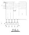
- a neural network component as shown in Figure 1 comprises 1024 inputs 1, a Random Access Memory (RAM) 2, 256 processing elements 3 and 256 outputs 4.
- RAM Random Access Memory
- Each input carries a signal from a processing element of a previous neural network component.
- Each input carries only 1 bit of information, in other words it is either 'on' or 'off'.
- Input signals take the form of pulses on the inputs.
- the RAM 2 contains a set of values. A different address in the RAM is allocated to each combination of input and output (the number of addresses is 1024x256).
- the RAM may be considered to be a two dimensional matrix comprising columns and rows, each row containing all of the values pertaining to a particular input, and each column containing all of the values pertaining to a particular processing element. As discussed further below, a significant proportion of the RAM addresses may contain zero values.
- the RAM 2 looks up values located in the row corresponding to that input. Each value is passed to the processing element 3 corresponding to the column in which that value is located. The activation level of the processing element 3 (an internal measurement of the state of the processing element) is modified in accordance with the value that is received. Each processing element 3 acts as a neuron, and has 1024 inputs and 1 output.
- the values stored in the RAM 2 may be weights or they may be instructions. Where the value passed to a processing element 3 is an instruction, the processing element 3 carries out an operation in accordance with the instruction, as described further below. Where the value passed to the processing element 3 is a weight, that weight is added to the activation level of the processing element 3.
- X j are inputs to the neuron
- W ij are the weights
- the sum ⁇ j W ij ⁇ X j is the activation level of the neuron
- T i is the threshold of the processing element
- f i is an activation function (this is usually non-linear)
- Y i is the output of ith processing element.
- a pulse is output by the processing element when the activation level exceeds the threshold (this is in effect the firing of the neuron).
- j which designates a specific input may be between 1 and 1024
- i which designates a specific output may be between 1 and 256.
- Y i of a neuron would be a number having a value between 0 and 1. This output, when input to a subsequent neuron would be multiplied by a weight, and the result of the multiplication added to the activation level of that subsequent neuron.
- the described embodiment of the invention operates in a different manner to analogue neural networks, in that a processing element (neuron) has only two possible outputs, i.e. 1 or 0 (or equivalently 'on' or 'off').
- An output pulse is generated by a processing element whenever the activation level of that processing element exceeds its threshold. From an outside observer's point of view, a pulsed output of a processing element may be considered to be equivalent to an analogue output. For example, if a processing element were to generate 23 pulses in one second, then this could be considered to be equivalent to a notional analogue value of 0.23.
- the generation of pulses by the processing elements is referred to hereafter as 'pulse rate encoding'.
- pulse rate encoding is very computationally intensive when compared to the use of analogue signals. For example, a weight allocated to a given input of a neuron may be multiplied by the analogue signal 0.23 in a single calculation, and then added to the activation level of the neuron. In contrast to this, when using pulse rate encoding the weight must be added to the activation level of the neuron 23 times (i.e. once per pulse), requiring 23 separate calculations. It is noted however that there is often no output from a given neuron. Where pulse rate encoding is used, no calculations are carried out in this eventuality since no input pulses are received.
- a zero value of output is effectively an output value that happens to be zero.
- the weights of the neurons are multiplied by the zero output value, and the result (also zero) is added to the activation levels of the neurons.
- This calculation which has no effect on the activation levels of the neurons occurs very frequently and is computationally very wasteful.
- the use of pulse rate encoding avoids this wasteful multiplication by zero.
- the neural network component is provided with 256 processing elements 3.
- Each processing element 3 acts as a neuron, and has 1024 inputs and 1 output. If individual connections were to be provided between each processing element and each subsequent neural network component, then the number of connections would rapidly become so large as to be impractical.
- the outputs from the processing elements are all directed into a single 8-bit output line 5.
- An output pulse from a given processing element is converted into an 8-bit binary number representative of that processing element, which is carried by the output line. This conversion, which may be referred to as 'addressed-event encoding' is carried out by an arbitration and encoding unit 6.
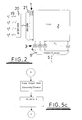
- the operation of the arbitration and encoding unit 6 is illustrated schematically in Figure 3 .
- the unit 6 has two functions: to determine the chronological order in which pulses are to be sent to the output line 5, and to convert each output into a number indicative of the processing element that generated that output. The two functions are achieved simultaneously by the unit 6.
- the unit 6 shown in Figure 3 is for a set of eight processing elements.
- a first tier of the unit 6 comprises four arbitration and encoding blocks 10-13.
- An input side of a first arbitration and encoding block 10 is provided with two inputs a, b and two acknowledge outputs a ack , b ack .
- a first output y of the block 10 goes high, and a second output z simultaneously outputs a 1-bit number representative of input a (in this case the binary number is '1').
- the acknowledge output a ack then goes high, thereby indicating to the processing element that the output has been processed by the block 10.
- the output of the processing element then goes low.
- a Seitz mutual exclusion element determines which input was the first to go high (Mutual exclusion elements are described at pages 260 et seq. of 'Introduction to VLSI systems' by Mead and Conway, published by Addison Wesley). Output from the block 10 is generated accordingly. Once the output has been generated, and an acknowledge sent back to the appropriate processing element, the later of the inputs is processed and output by the block 10.
- a second tier of the unit 6 comprises a pair of arbitration and encoding blocks 14,15.
- a first block 14 of the pair two inputs y, w are connected to outputs of preceding blocks 10, 11.
- a first output u of the block 14 goes high in response to an input signal, and a second output v simultaneously outputs a 2-bit number.
- the most significant bit of the 2-bit number represents the input y, and the least significant bit of the 2-bit number represents the input a of the preceding block 10.
- the 2-bit number is the binary number '11'.
- the third and final tier of the unit 6 operates in the same manner as the previous tiers.
- the output from the single block 16 comprising the final tier is a 3-bit binary number, and in this case is the number '111'.
- the output from a processing element 3 is said to be in the form of a pulse. It will be noted that in the description of Figure 3 the output from the processing element is said to be a continuous high which ends only after an acknowledge signal has been received by the processing element. This modification is required in order to allow the arbitration and encoding unit 6 to function correctly.
- FIG. 2 four 8-bit input lines 19 are connected to the processing elements 3 and RAM 2.
- An arbitration and encoding unit 20 is used to arbitrate between the four input lines 19.
- the arbitration and encoding unit 20 operates the manner shown schematically in Figure 2 and described above. In this case the arbitration and encoding unit includes two tiers of blocks.
- the arbitration and encoding unit has a 10-bit output, the extra two bits being used to distinguish between the four 8-bit input lines 19.
- the 10-bit output of the arbitration and encoding unit 20 is connected to a decoder 21.
- the decoder converts each received 10-bit input number to an output on a corresponding 1-bit output line 1 (there are 1024 output lines).
- the output lines 1 correspond to the input lines 1 shown in Figure 1 .
- the neural network component is digital provides a degree of flexibility not seen in analogue neural network components.
- a large range of values may be stored in the RAM 2, and this allows some of the values to be used as 'instructions' for the processing elements 3.
- the term 'instruction' is intended to mean that the processing element is instructed to carry out an operation other than simply adding a value to the activation level.
- the action carried out by a neuron is always the same, i.e. to add a value to the activation level.
- the use of instructions allows the processing elements 3 to have much more flexibility in their operation.
- the use of instructions provides a neural network having properties which are closer to biologically realistic neurons.
- One such property is a 'leaky' integration, in other words an activation level which decays if there is no input activity over a period of time.
- Another property is 'refraction', meaning that a processing element 3 ignores all inputs for a certain period following firing. This limits the processing element's maximum firing rate (i.e. the rate at which the processing element 3 can produce output pulses), thereby preventing the network from becoming unstable due to ever-increasing neuronal activity. Both refraction and leaky integration imply some dependence on real time.
- Refraction and leaky integration are provided in the described embodiment of the invention using a real-time reference event, for example a 32 kHz clock (not shown in Figures 1 or 2 ). Pulses from the clock may transmitted as a particular binary number via the 8-bit input (for example 00000001). Where leaky integration is required, the value stored in each RAM address corresponding to this input number will instruct the processing element to decrement its activation level if the activation level is positive and increment the activation level if it is negative. Different values held in the RAM may instruct different rates of leaky integration, for example increment/decrement in response to every clock pulse, or increment/decrement in response to every second clock pulse.
- An instruction may be provided which determines whether or not the weight should be adjusted by automatic learning algorithms (for example Hebbian learning algorithms).
- automatic learning algorithms for example Hebbian learning algorithms.
- the following neuron behaviour can be modelled as shown in Figure 4 .
- the activation level of the processing element operates within the range ⁇ -L, +T ⁇ , where -L is the refractory level and T is the threshold which, when reached, causes the processing element to output a pulse and the activation level to be reset to -L.
- ⁇ -L, 0 ⁇ is the refractory range of the processing element: if a weight is passed to the processing element in response to an input pulse, the weight is not added to the activation level (the activation level is unchanged), and the weight itself is decremented.
- ⁇ 0, F ⁇ is the weakly excited range: : if a weight is passed to the processing element in response to an input pulse it will be added to the activation level and the weight itself will be unchanged by the learning mechanism.
- ⁇ F, T ⁇ is the strongly excited range: if a weight is passed to the processing element in response to an input pulse it will be added to the activation level and the weight itself will be incremented.
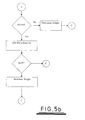
- a pulse is received at a given input j.
- the value associated with that input j for a given processing element is retrieved from the RAM and passed to the processing element.
- the value will fall within one of three ranges: a first range corresponds to weights which are to be added to the activation level, a second range corresponds to weights which are to be added to the activation level and in addition instruct the processing element that the weight associated with that input is to be incremented, and a third range comprises instructions other than weights.
- the remainder of Figure 5a deals with a value which falls within the first range.
- the value is added to the activation level of the processing element (the activation level will be reduced if the weight is negative). If the activation level following addition of the value is less than the threshold T then no further action is taken. If the activation level is greater than the threshold T, then the processing element outputs a pulse and the activation level of the processing element is reduced to -L.
- operation of the processing element as shown in the flow chart branches to Figure 5b . If the activation level of the processing element is greater than or equal to zero then the value is added to the activation level of the processing element. Following this, if the activation level is greater than F then the value saved in the RAM is incremented.
- the value is not added to the activation level, and the value saved in the RAM is decremented.
- the processing element may be instructed to emit a pulse irrespective of the activation level, and reset the activation level to the refractory level.
- This Hebbian learning algorithm which results in a stable neural network if appropriate values are chosen, depends on a mechanism to return the activation level from -L to 0 which is separate from the numerical weight processing, and therefore depends on the use of an 'increment towards zero over time' instruction which may be implemented as described above.
- the processing elements may be capable of executing other instructions, which may be defined by values stored in the RAM value memory.
- the activation level may be reset to the refractory level without firing the neuron. This models a strongly inhibitory input.
- the neural network component may include a conventional processor (not shown) with read-write access to the RAM value store 4.
- the processor may have the capability to monitor and generate input and output to neural activity streams, using suitable interface peripherals incorporated into the neural network component.
- Processor accesses to the RAM value store 4 and the neural activity streams can be arbitrated asynchronously into the fully operational network with minimal interference with the neural processing provided that the network is not operating near to saturation at the time.
- One monitor processor could supervise a number of neural network components, but a very large system may require several such processors.
- An implementation based on 1 Gbit DRAM technology might have a monitor processor on each chip.
- the neural network may be implemented as a very large number of neural network components supervised by a parallel network of conventional processors.
- the ease with which the architecture connects to conventional machines is a merit of the invention.
- the control processor greatly extends the flexibility of the architecture and provides a close coupling between the neural processing and a conventional, sequential machine.
- one processing element corresponds to one neuron
- a processing element may be responsible for performing the calculations for more than one neuron.
Landscapes
- Engineering & Computer Science (AREA)
- Physics & Mathematics (AREA)
- Health & Medical Sciences (AREA)
- Life Sciences & Earth Sciences (AREA)
- Biomedical Technology (AREA)
- Biophysics (AREA)
- Theoretical Computer Science (AREA)
- General Engineering & Computer Science (AREA)
- Neurology (AREA)
- Data Mining & Analysis (AREA)
- Evolutionary Computation (AREA)
- General Health & Medical Sciences (AREA)
- Molecular Biology (AREA)
- Computing Systems (AREA)
- Artificial Intelligence (AREA)
- General Physics & Mathematics (AREA)
- Mathematical Physics (AREA)
- Software Systems (AREA)
- Computational Linguistics (AREA)
- Image Analysis (AREA)
- Complex Calculations (AREA)
- Thermistors And Varistors (AREA)
- Magnetic Resonance Imaging Apparatus (AREA)
- Facsimile Image Signal Circuits (AREA)
- Image Processing (AREA)
- Transition And Organic Metals Composition Catalysts For Addition Polymerization (AREA)
- Polyethers (AREA)
- Circuit For Audible Band Transducer (AREA)
- Feedback Control In General (AREA)
Applications Claiming Priority (3)
| Application Number | Priority Date | Filing Date | Title |
|---|---|---|---|
| GBGB9924310.7A GB9924310D0 (en) | 1999-10-15 | 1999-10-15 | Neural network component |
| GB9924310 | 1999-10-15 | ||
| PCT/GB2000/003957 WO2001029766A2 (en) | 1999-10-15 | 2000-10-16 | Neural network component |
Publications (2)
| Publication Number | Publication Date |
|---|---|
| EP1224619A2 EP1224619A2 (en) | 2002-07-24 |
| EP1224619B1 true EP1224619B1 (en) | 2010-02-10 |
Family
ID=10862720
Family Applications (1)
| Application Number | Title | Priority Date | Filing Date |
|---|---|---|---|
| EP00968107A Expired - Lifetime EP1224619B1 (en) | 1999-10-15 | 2000-10-16 | Neural network component |
Country Status (9)
| Country | Link |
|---|---|
| US (1) | US7457787B1 (enExample) |
| EP (1) | EP1224619B1 (enExample) |
| JP (1) | JP4931311B2 (enExample) |
| AT (1) | ATE457503T1 (enExample) |
| AU (1) | AU7806500A (enExample) |
| DE (1) | DE60043824D1 (enExample) |
| ES (1) | ES2338751T3 (enExample) |
| GB (1) | GB9924310D0 (enExample) |
| WO (1) | WO2001029766A2 (enExample) |
Families Citing this family (14)
| Publication number | Priority date | Publication date | Assignee | Title |
|---|---|---|---|---|
| US8515885B2 (en) | 2010-10-29 | 2013-08-20 | International Business Machines Corporation | Neuromorphic and synaptronic spiking neural network with synaptic weights learned using simulation |
| US8812414B2 (en) | 2011-05-31 | 2014-08-19 | International Business Machines Corporation | Low-power event-driven neural computing architecture in neural networks |
| US8843425B2 (en) * | 2011-07-29 | 2014-09-23 | International Business Machines Corporation | Hierarchical routing for two-way information flow and structural plasticity in neural networks |
| US8909576B2 (en) * | 2011-09-16 | 2014-12-09 | International Business Machines Corporation | Neuromorphic event-driven neural computing architecture in a scalable neural network |
| US8924322B2 (en) * | 2012-06-15 | 2014-12-30 | International Business Machines Corporation | Multi-processor cortical simulations with reciprocal connections with shared weights |
| US9218564B2 (en) | 2012-07-30 | 2015-12-22 | International Business Machines Corporation | Providing transposable access to a synapse array using a recursive array layout |
| US8918351B2 (en) | 2012-07-30 | 2014-12-23 | International Business Machines Corporation | Providing transposable access to a synapse array using column aggregation |
| US9159020B2 (en) | 2012-09-14 | 2015-10-13 | International Business Machines Corporation | Multiplexing physical neurons to optimize power and area |
| US8990130B2 (en) | 2012-11-21 | 2015-03-24 | International Business Machines Corporation | Consolidating multiple neurosynaptic cores into one memory |
| US9558443B2 (en) | 2013-08-02 | 2017-01-31 | International Business Machines Corporation | Dual deterministic and stochastic neurosynaptic core circuit |
| US9852006B2 (en) | 2014-03-28 | 2017-12-26 | International Business Machines Corporation | Consolidating multiple neurosynaptic core circuits into one reconfigurable memory block maintaining neuronal information for the core circuits |
| US10410109B2 (en) | 2014-08-25 | 2019-09-10 | International Business Machines Corporation | Peripheral device interconnections for neurosynaptic systems |
| US11093830B2 (en) | 2018-01-30 | 2021-08-17 | D5Ai Llc | Stacking multiple nodal networks |
| WO2019152308A1 (en) * | 2018-01-30 | 2019-08-08 | D5Ai Llc | Self-organizing partially ordered networks |
Family Cites Families (13)
| Publication number | Priority date | Publication date | Assignee | Title |
|---|---|---|---|---|
| US5148385A (en) * | 1987-02-04 | 1992-09-15 | Texas Instruments Incorporated | Serial systolic processor |
| JP2588195B2 (ja) * | 1987-05-28 | 1997-03-05 | 株式会社東芝 | パルス入力装置 |
| JP2804069B2 (ja) * | 1989-03-10 | 1998-09-24 | 株式会社日立製作所 | 情報処理装置 |
| JPH02310666A (ja) * | 1989-05-25 | 1990-12-26 | Mitsubishi Electric Corp | 半導体神経回路装置 |
| JP3210319B2 (ja) | 1990-03-01 | 2001-09-17 | 株式会社東芝 | ニューロチップおよびそのチップを用いたニューロコンピュータ |
| DE4215179A1 (de) * | 1991-05-08 | 1992-11-12 | Caterpillar Inc | Prozessor und verarbeitendes element zum gebrauch in einem neural- oder nervennetzwerk |
| US6894639B1 (en) * | 1991-12-18 | 2005-05-17 | Raytheon Company | Generalized hebbian learning for principal component analysis and automatic target recognition, systems and method |
| US5278945A (en) * | 1992-01-10 | 1994-01-11 | American Neuralogical, Inc. | Neural processor apparatus |
| US5404556A (en) * | 1992-06-15 | 1995-04-04 | California Institute Of Technology | Apparatus for carrying out asynchronous communication among integrated circuits |
| US5920852A (en) * | 1996-04-30 | 1999-07-06 | Grannet Corporation | Large memory storage and retrieval (LAMSTAR) network |
| JPH1091605A (ja) * | 1997-05-09 | 1998-04-10 | Hitachi Ltd | 情報処理装置 |
| IL133384A0 (en) * | 1997-06-11 | 2001-04-30 | Univ Southern California | Dynamic synapse for signal processing in neural networks |
| US6516309B1 (en) * | 1998-07-17 | 2003-02-04 | Advanced Research & Technology Institute | Method and apparatus for evolving a neural network |
-
1999
- 1999-10-15 GB GBGB9924310.7A patent/GB9924310D0/en not_active Ceased
-
2000
- 2000-10-16 AU AU78065/00A patent/AU7806500A/en not_active Abandoned
- 2000-10-16 AT AT00968107T patent/ATE457503T1/de not_active IP Right Cessation
- 2000-10-16 WO PCT/GB2000/003957 patent/WO2001029766A2/en not_active Ceased
- 2000-10-16 JP JP2001532486A patent/JP4931311B2/ja not_active Expired - Fee Related
- 2000-10-16 DE DE60043824T patent/DE60043824D1/de not_active Expired - Lifetime
- 2000-10-16 EP EP00968107A patent/EP1224619B1/en not_active Expired - Lifetime
- 2000-10-16 ES ES00968107T patent/ES2338751T3/es not_active Expired - Lifetime
- 2000-10-16 US US10/110,477 patent/US7457787B1/en not_active Expired - Fee Related
Also Published As
| Publication number | Publication date |
|---|---|
| AU7806500A (en) | 2001-04-30 |
| JP2003512683A (ja) | 2003-04-02 |
| US7457787B1 (en) | 2008-11-25 |
| ES2338751T3 (es) | 2010-05-12 |
| JP4931311B2 (ja) | 2012-05-16 |
| ATE457503T1 (de) | 2010-02-15 |
| DE60043824D1 (de) | 2010-03-25 |
| GB9924310D0 (en) | 1999-12-15 |
| WO2001029766A2 (en) | 2001-04-26 |
| WO2001029766A3 (en) | 2002-04-25 |
| EP1224619A2 (en) | 2002-07-24 |
Similar Documents
| Publication | Publication Date | Title |
|---|---|---|
| EP1224619B1 (en) | Neural network component | |
| KR102592146B1 (ko) | 시냅스 가중치 학습을 위한 뉴런 회로, 시스템 및 방법 | |
| US10628732B2 (en) | Reconfigurable and customizable general-purpose circuits for neural networks | |
| EP2641214B1 (en) | Electronic synapses for reinforcement learning | |
| Rao | Bayesian computation in recurrent neural circuits | |
| JP5963315B2 (ja) | シミュレーションを使用して学習されるシナプス重みを用いるニューロモーフィック/シナプトロニック・スパイキング・ニューラル・ネットワークのための方法、デバイス、および回路 | |
| US4518866A (en) | Method of and circuit for simulating neurons | |
| US8812414B2 (en) | Low-power event-driven neural computing architecture in neural networks | |
| EP0327817B1 (en) | Associative pattern conversion system and adaptation method thereof | |
| US10198692B2 (en) | Scalable neural hardware for the noisy-OR model of Bayesian networks | |
| US20190138900A1 (en) | Neuron circuit, system, and method with synapse weight learning | |
| EP2849083A1 (en) | Method and system for converting pulsed-processing neural network with instantaneous integration synapses into dynamic integration synapses | |
| JP2512263B2 (ja) | 畳込みエキスパ―ト神経システム | |
| CN113723594A (zh) | 一种脉冲神经网络目标识别方法 | |
| CN114897152B (zh) | 一种神经形态计算装置 | |
| KR102419338B1 (ko) | 스파이킹 신경망 학습 장치 및 방법 | |
| CN112598119A (zh) | 一种面向液体状态机的神经形态处理器片上存储压缩方法 | |
| WO2004027704A1 (en) | Spiking neural network device | |
| CN115545178B (zh) | 一种减小脉冲神经网络神经元计算次数的硬件实现方法 | |
| CN113011572B (zh) | 一种轴突变化量确定方法和装置、权重处理方法和装置 | |
| Stoianov et al. | Associative arithmetic with Boltzmann Machines: The role of number representations | |
| Sayarkin et al. | Spiking neural network model MATLAB implementation based on Izhikevich mathematical model for control systems | |
| US4841473A (en) | Computer architecture providing programmable degrees of an almost condition | |
| JP3117204B2 (ja) | 制御物理変量発生用および物体識別用ニューラル・ネット | |
| KR102514655B1 (ko) | 스파이크 신호를 병렬처리하는 뉴로모픽 장치 |
Legal Events
| Date | Code | Title | Description |
|---|---|---|---|
| PUAI | Public reference made under article 153(3) epc to a published international application that has entered the european phase |
Free format text: ORIGINAL CODE: 0009012 |
|
| 17P | Request for examination filed |
Effective date: 20020419 |
|
| AK | Designated contracting states |
Kind code of ref document: A2 Designated state(s): AT BE CH CY DE DK ES FI FR GB GR IE IT LI LU MC NL |
|
| AX | Request for extension of the european patent |
Free format text: AL;LT;LV;MK;RO;SI |
|
| RAP1 | Party data changed (applicant data changed or rights of an application transferred) |
Owner name: THE UNIVERSITY OF MANCHESTER |
|
| 17Q | First examination report despatched |
Effective date: 20061005 |
|
| GRAP | Despatch of communication of intention to grant a patent |
Free format text: ORIGINAL CODE: EPIDOSNIGR1 |
|
| GRAS | Grant fee paid |
Free format text: ORIGINAL CODE: EPIDOSNIGR3 |
|
| GRAA | (expected) grant |
Free format text: ORIGINAL CODE: 0009210 |
|
| AK | Designated contracting states |
Kind code of ref document: B1 Designated state(s): AT BE CH CY DE DK ES FI FR GB GR IE IT LI LU MC NL |
|
| REG | Reference to a national code |
Ref country code: GB Ref legal event code: FG4D |
|
| REG | Reference to a national code |
Ref country code: CH Ref legal event code: EP |
|
| REG | Reference to a national code |
Ref country code: IE Ref legal event code: FG4D |
|
| REF | Corresponds to: |
Ref document number: 60043824 Country of ref document: DE Date of ref document: 20100325 Kind code of ref document: P |
|
| REG | Reference to a national code |
Ref country code: ES Ref legal event code: FG2A Ref document number: 2338751 Country of ref document: ES Kind code of ref document: T3 |
|
| REG | Reference to a national code |
Ref country code: NL Ref legal event code: VDEP Effective date: 20100210 |
|
| PG25 | Lapsed in a contracting state [announced via postgrant information from national office to epo] |
Ref country code: FI Free format text: LAPSE BECAUSE OF FAILURE TO SUBMIT A TRANSLATION OF THE DESCRIPTION OR TO PAY THE FEE WITHIN THE PRESCRIBED TIME-LIMIT Effective date: 20100210 Ref country code: AT Free format text: LAPSE BECAUSE OF FAILURE TO SUBMIT A TRANSLATION OF THE DESCRIPTION OR TO PAY THE FEE WITHIN THE PRESCRIBED TIME-LIMIT Effective date: 20100210 |
|
| PG25 | Lapsed in a contracting state [announced via postgrant information from national office to epo] |
Ref country code: GR Free format text: LAPSE BECAUSE OF FAILURE TO SUBMIT A TRANSLATION OF THE DESCRIPTION OR TO PAY THE FEE WITHIN THE PRESCRIBED TIME-LIMIT Effective date: 20100511 Ref country code: CY Free format text: LAPSE BECAUSE OF FAILURE TO SUBMIT A TRANSLATION OF THE DESCRIPTION OR TO PAY THE FEE WITHIN THE PRESCRIBED TIME-LIMIT Effective date: 20100210 Ref country code: BE Free format text: LAPSE BECAUSE OF FAILURE TO SUBMIT A TRANSLATION OF THE DESCRIPTION OR TO PAY THE FEE WITHIN THE PRESCRIBED TIME-LIMIT Effective date: 20100210 Ref country code: NL Free format text: LAPSE BECAUSE OF FAILURE TO SUBMIT A TRANSLATION OF THE DESCRIPTION OR TO PAY THE FEE WITHIN THE PRESCRIBED TIME-LIMIT Effective date: 20100210 |
|
| PLBE | No opposition filed within time limit |
Free format text: ORIGINAL CODE: 0009261 |
|
| STAA | Information on the status of an ep patent application or granted ep patent |
Free format text: STATUS: NO OPPOSITION FILED WITHIN TIME LIMIT |
|
| 26N | No opposition filed |
Effective date: 20101111 |
|
| PG25 | Lapsed in a contracting state [announced via postgrant information from national office to epo] |
Ref country code: DK Free format text: LAPSE BECAUSE OF FAILURE TO SUBMIT A TRANSLATION OF THE DESCRIPTION OR TO PAY THE FEE WITHIN THE PRESCRIBED TIME-LIMIT Effective date: 20100210 |
|
| PG25 | Lapsed in a contracting state [announced via postgrant information from national office to epo] |
Ref country code: MC Free format text: LAPSE BECAUSE OF NON-PAYMENT OF DUE FEES Effective date: 20101031 |
|
| REG | Reference to a national code |
Ref country code: CH Ref legal event code: PL |
|
| PG25 | Lapsed in a contracting state [announced via postgrant information from national office to epo] |
Ref country code: LI Free format text: LAPSE BECAUSE OF NON-PAYMENT OF DUE FEES Effective date: 20101031 Ref country code: CH Free format text: LAPSE BECAUSE OF NON-PAYMENT OF DUE FEES Effective date: 20101031 |
|
| PG25 | Lapsed in a contracting state [announced via postgrant information from national office to epo] |
Ref country code: IE Free format text: LAPSE BECAUSE OF NON-PAYMENT OF DUE FEES Effective date: 20101016 |
|
| PG25 | Lapsed in a contracting state [announced via postgrant information from national office to epo] |
Ref country code: LU Free format text: LAPSE BECAUSE OF NON-PAYMENT OF DUE FEES Effective date: 20101016 |
|
| PGFP | Annual fee paid to national office [announced via postgrant information from national office to epo] |
Ref country code: ES Payment date: 20140911 Year of fee payment: 15 |
|
| PGFP | Annual fee paid to national office [announced via postgrant information from national office to epo] |
Ref country code: GB Payment date: 20141015 Year of fee payment: 15 Ref country code: FR Payment date: 20141008 Year of fee payment: 15 Ref country code: DE Payment date: 20141007 Year of fee payment: 15 |
|
| PGFP | Annual fee paid to national office [announced via postgrant information from national office to epo] |
Ref country code: IT Payment date: 20141020 Year of fee payment: 15 |
|
| REG | Reference to a national code |
Ref country code: DE Ref legal event code: R119 Ref document number: 60043824 Country of ref document: DE |
|
| GBPC | Gb: european patent ceased through non-payment of renewal fee |
Effective date: 20151016 |
|
| PG25 | Lapsed in a contracting state [announced via postgrant information from national office to epo] |
Ref country code: DE Free format text: LAPSE BECAUSE OF NON-PAYMENT OF DUE FEES Effective date: 20160503 Ref country code: GB Free format text: LAPSE BECAUSE OF NON-PAYMENT OF DUE FEES Effective date: 20151016 Ref country code: IT Free format text: LAPSE BECAUSE OF NON-PAYMENT OF DUE FEES Effective date: 20151016 |
|
| REG | Reference to a national code |
Ref country code: FR Ref legal event code: ST Effective date: 20160630 |
|
| PG25 | Lapsed in a contracting state [announced via postgrant information from national office to epo] |
Ref country code: FR Free format text: LAPSE BECAUSE OF NON-PAYMENT OF DUE FEES Effective date: 20151102 |
|
| REG | Reference to a national code |
Ref country code: ES Ref legal event code: FD2A Effective date: 20161129 |
|
| PG25 | Lapsed in a contracting state [announced via postgrant information from national office to epo] |
Ref country code: ES Free format text: LAPSE BECAUSE OF NON-PAYMENT OF DUE FEES Effective date: 20151017 |