EP1223746A2 - Active pixel image sensor with improved linearity - Google Patents
Active pixel image sensor with improved linearity Download PDFInfo
- Publication number
- EP1223746A2 EP1223746A2 EP01204939A EP01204939A EP1223746A2 EP 1223746 A2 EP1223746 A2 EP 1223746A2 EP 01204939 A EP01204939 A EP 01204939A EP 01204939 A EP01204939 A EP 01204939A EP 1223746 A2 EP1223746 A2 EP 1223746A2
- Authority
- EP
- European Patent Office
- Prior art keywords
- voltage
- capacitance
- capacitor
- charge
- transistor
- Prior art date
- Legal status (The legal status is an assumption and is not a legal conclusion. Google has not performed a legal analysis and makes no representation as to the accuracy of the status listed.)
- Granted
Links
Images


Classifications
-
- H—ELECTRICITY
- H04—ELECTRIC COMMUNICATION TECHNIQUE
- H04N—PICTORIAL COMMUNICATION, e.g. TELEVISION
- H04N25/00—Circuitry of solid-state image sensors [SSIS]; Control thereof
- H04N25/50—Control of the SSIS exposure
- H04N25/57—Control of the dynamic range
- H04N25/59—Control of the dynamic range by controlling the amount of charge storable in the pixel, e.g. modification of the charge conversion ratio of the floating node capacitance
-
- H—ELECTRICITY
- H04—ELECTRIC COMMUNICATION TECHNIQUE
- H04N—PICTORIAL COMMUNICATION, e.g. TELEVISION
- H04N25/00—Circuitry of solid-state image sensors [SSIS]; Control thereof
- H04N25/70—SSIS architectures; Circuits associated therewith
- H04N25/76—Addressed sensors, e.g. MOS or CMOS sensors
- H04N25/77—Pixel circuitry, e.g. memories, A/D converters, pixel amplifiers, shared circuits or shared components
- H04N25/771—Pixel circuitry, e.g. memories, A/D converters, pixel amplifiers, shared circuits or shared components comprising storage means other than floating diffusion
-
- H—ELECTRICITY
- H04—ELECTRIC COMMUNICATION TECHNIQUE
- H04N—PICTORIAL COMMUNICATION, e.g. TELEVISION
- H04N25/00—Circuitry of solid-state image sensors [SSIS]; Control thereof
- H04N25/70—SSIS architectures; Circuits associated therewith
- H04N25/76—Addressed sensors, e.g. MOS or CMOS sensors
Definitions
- the present invention generally relates to complementary metal oxide semiconductor (CMOS) active pixel sensors (APS) and more particularly to an improved pixel sensor that has increased linearity as a result of additional voltage-independent capacitance.
- CMOS complementary metal oxide semiconductor
- APS active pixel sensors
- CMOS APS are solid state imagers where each pixel contains a photo-sensing means, reset means, charge conversion means, select means, and all or part of an amplifier. APS devices have the advantages of single supply operation, lower power consumption, x-y addressability, image windowing, and the ability to effectively integrate signal processing electronics on-chip, when compared to CCD sensors.
- CMOS complementary metal-oxide-semiconductor
- the integrated photoelectrons are converted to a voltage in each pixel.
- This charge to voltage conversion region is typically a diode, either the photodiode or an isolated floating diffusion. It is the parasitic capacitance of the charge to voltage conversion region that determines the maximum number of electrons that can be contained within the region.
- CMOS processes are typically operated at low supply voltages, 3.3V and below, hence the reset level and the voltage swing that can be accommodated in the charge to voltage conversion region is limited by the supply voltage. Since the supply voltage is low, the signal swing on the charge to voltage conversion region is a large compared to the reset level. Since the capacitance of the diode that forms the charge to voltage conversion region is a function of the voltage across the diode, and the signal swing is large compared to the total voltage across the diode at reset, the capacitance of the diode changes substantially from the reset level, (or dark signal), to the saturation level, (or bright signal). In typical APS pixel architectures the capacitance at reset is smaller than the capacitance at saturation.
- CMOS APS sensors can also suffer from low charge capacity as a result of the reduced supply voltages in sub- ⁇ m CMOS processes.
- CMOS APS sensors have lower charge capacity compared to CCD image sensors due to the larger supply and clock voltages used on CCD image sensors.
- One approach to providing an image sensor with the linearity of a CCD and the advantages of an APS device is to reduce the effect of the voltage dependent capacitance of the charge to voltage conversion region of an APS device.
- This invention does so by providing a voltage independent capacitor in parallel with the diode capacitance of the charge to voltage conversion region. This can also be used to improve the charge capacity of an APS device.
- an object of the present invention to provide a structure and method for a complementary metal oxide semiconductor active pixel sensor device having a photodetector, a charge to voltage conversion node, an amplifier input connected to the charge to voltage conversion node, and a voltage-independent capacitance connected in parallel with the charge to voltage conversion node.
- the voltage-independent capacitance provides a capacitance that is not a function of charge placed on the charge to voltage conversion node.
- the voltage-independent capacitance can be an electrode-electrode capacitor, or the input capacitance of an amplifier.
- the invention also comprises a method of manufacturing a complementary metal oxide semiconductor active pixel sensor device which includes a photodetector, a charge to voltage conversion node, an amplifier input connected to the charge to voltage conversion node, and a voltage-independent capacitance connected in parallel with the charge to voltage conversion node.
- the voltage-independent capacitance provides a capacitance that is not a function of charge placed on the charge to voltage conversion node.
- the voltage-independent capacitance can be an electrode-electrode capacitor, or the input capacitance of an amplifier.
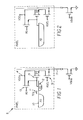
- FIG. 1 is a schematic diagram that illustrates a CMOS APS pixel 5.
- the cell 5 includes a photodiode 10, a transfer transistor 11 with a transfer gate TG, whose source is connected to the photodiode, and a reset transistor 13 with a reset gate RG, whose drain is connected to the voltage supply VDD 14.
- the drains of the transfer transistor 11 and the source of the reset transistor 13 form a floating diffusion region FD 12 which functions as a charge to voltage conversion node.
- the floating diffusion region 12 is connected to the gate of the input transistor 15 of a source follower amplifier.
- the source of the input transistor 15 is connected to the drain of the row select transistor 16, and the source of row select transistor 16 is connected to the column bus 17.
- Operation of active pixel sensor cell 5 is performed in three steps: a reset step, where cell 10 is reset from the previous integration cycle; an image integration step, where the light energy is collected and converted into an electrical signal; and a signal readout step, where the signal is read out.
- the gate of reset transistor 13, and transfer transistor 11 is briefly pulsed with a reset voltage (e.g. 3.3 volts).
- the reset voltage turns on reset transistor 13 and transfer transistor 11 which pulls up the voltage on photodiode 10, and floating diffusion region 12 to an initial reset voltage.
- the integration phase can commence.
- light energy in the form of photons, strikes photodiode 10, thereby creating a number of electron-hole pairs.
- Photodiode 10 is designed to limit recombination between the newly formed electron-hole pairs.
- the photo-generated holes are attracted to the ground terminal of photodiode 10, while the photo-generated electrons are attracted to the positive terminal of photodiode 10 where each additional electron reduces the voltage on photodiode 10.
- the potential on photodiode 10 will have been reduced to a final integration voltage where the amount of the reduction represents the intensity of the received light energy.
- First row select transistor 16 is turned on by applying a select voltage, (e.g. 3.3 volts) to the gate of row select transistor 16.
- a select voltage e.g. 3.3 volts
- the gate of reset transistor 13 is briefly pulsed with a reset voltage (e.g. 3.3 volts).
- the reset voltage turns on reset transistor 13 which pulls up the voltage on floating diffusion 12 to an initial reset voltage, typically less than or equal to VDD minus the reset transistor threshold voltage.
- the floating diffusion reset voltage on the gate of source of source-follower transistor 15 is then read out as a reset voltage level.
- the integrated photo-electrons are transferred from the photodetector to the floating diffusion by pulsing the gate of transfer transistor 11. This reduces the voltage on the floating diffusion 12.
- the floating diffusion signal voltage on the gate of source-follower transistor 15 is then read out as a signal voltage level.
- the signal and reset levels are then subtracted providing a voltage which represents the total charge collected by cell 5.
- the maximum number of photo-electrons or maximum signal level typically reduces the floating diffusion voltage level by an amount that is all of, or a large percentage of the reset voltage on the floating diffusion.
- the floating diffusion depletion region width changes by a substantial amount compared to the initial depletion region width after reset. This produces a variable floating diffusion capacitance that is a function of the number of photo-electrons transferred to the floating diffusion.
- the floating diffusion depletion region width decreases and the floating diffusion capacitance increases. This produces a continuously non-linear transfer function.
- FIG. 3 The linearity problems created by voltage-dependent capacitance are illustrated in Figure 3.
- the vertical axis in Figure 3 represents the voltage of the floating diffusion region 12 while the horizontal axis represents the light level or integration time.
- the number of photo-electrons that are collected vs. light level or integration time is a linear relationship.
- the floating diffusion capacitance increases as a function of the number of photo-electrons collected, the output signal provided to the column bus 17 from the floating diffusion region vs. light level or integration time is not a linear relationship.
- line A represents a continuously non-linear transfer function.
- This line has a continuously negative second derivative.
- Line A has a useable signal range 33 up to the voltage level Vsat', based upon a certain percentage deviation from a linear transfer function. This is can be much less than the total signal swing Vsat. While the amount of light energy (e.g., photons) received along the second portion 30 of the response line can be calculated, such calculations can result in higher noise in the rendered image. Therefore, for high image quality applications, the APS pixel output is only used for voltages along the first portion of 33 and not generally utilized for voltages above Vsat'.
- the photodiode also functions as the charge to voltage conversion node, and its diode capacitance comprises a much larger portion of the total capacitance associated with electrical node of the gate of the source follower input transistor.
- the first portion of the pixel response transfer curve 33 is much smaller than that for the case the case of the APS pixel shown in Figure 1.
- the invention mitigates these problems by reducing the percentage of the voltage-dependent capacitance compared with the total capacitance associated with the charge to voltage conversion node. More specifically, the invention reduces the percentage of the voltage-dependent capacitance by including a larger voltage-independent capacitance connected to the charge to voltage conversion node.
- a capacitor C 1 50 is connected to the charge to voltage conversion node 12.
- the capacitor C 1 50 is selected to have a very low voltage coefficient to provide linearity and charge capacity for the reasons stated above. More specifically, by adding additional non-voltage-dependent capacitance, the linearity and saturation voltage is increased.
- the capacitor 50 comprises a polysilicon-polysilicon or other electrode-electrode capacitor. Such capacitors exhibit very low voltage coefficients and provide a capacitance that is independent of the voltage on the sensing node 12.
- the dotted line B in Figure 3 illustrates the pixel response transfer function achieved by adding a voltage-independent capacitance in parallel with the floating diffusion.
- the Vsat has decreased, since a fixed number of maximum electrons from the photodetector are converted to a voltage by a larger capacitance, the useful linear signal level Vsat', and linear signal transfer function 32, can be increased, while the second non-linear portion 31 is decreased.
- the overall charge capacity of the sensing node is increased, which is useful for cases where a large pixel and large photodetector are required.
- the linear signal response (e.g., portion 32) of the APS is dramatically increased because the overall voltage dependency capacitance of the cell is reduced by adding voltage-independent capacitance device(s).
- a combination of devices can be used to add voltage-independent capacitance to the APS.
- multiple capacitors 50 could be used to achieve the necessary level of capacitance.
- the invention utilizes a common source amplifier 40 as the readout mechanism, rather than the source follower 15 (e.g., see Figure 5a and 5b).
- the load for the common source amplifier 40 is shown as item 41 along the column bus 17.
- the input capacitance of a common source amplifier can be made larger than that of a source follower amplifier by designing the common source amplifier voltage gain to be greater than 1.
- the input capacitance of the common source amplifier 40 is preferably larger than that of the source follower amplifier so that the sense node junction capacitance is a smaller component of the overall capacitance of the sense node to improve linearity, and so the total capacitance is larger to provide larger charge capacity on the sense node.
- the input capacitance of the common source amplifier 40 can be made (selected) larger by designing the common-source amplifier voltage gain to provide the desired Miller effect on the gate-drain capacitance and the gate-channel capacitance of the pixel input transistor.
- a combination of the common source amplifier 40 and one or more capacitors 50 could be used to achieve the reduction in the percentage of the of voltage-dependent capacitance of the sense node, and the corresponding increase in linear signal response discussed above.
- capacitor C 1 could be comprise a capacitance to a node other than ground, such as VDD.
- the invention produces a greater linear signal response (e.g., portion 32) to light levels and has a higher voltage saturation level V sat2 because the voltage dependent capacitance of the cell is reduced by adding voltage-independent capacitance devices (40, 50).
Landscapes
- Engineering & Computer Science (AREA)
- Multimedia (AREA)
- Signal Processing (AREA)
- Solid State Image Pick-Up Elements (AREA)
- Transforming Light Signals Into Electric Signals (AREA)
Abstract
Description
Claims (10)
- An active pixel image sensor comprised of a plurality of pixels, at least one pixel comprising:a photodetector;a transistor;a charge to voltage conversion region coupled to said photodetector and connected to the input of said transistor; anda capacitor connected in parallel with the charge to voltage conversion region wherein the capacitor is designed to have a low voltage coefficient.
- The device in claim 1, wherein said capacitor provides a capacitance independently of a voltage on said charge to voltage conversion node.
- The device in claim 1, wherein said capacitor comprises a polysilicon to polysilicon double plate capacitor.
- The device in claim 1, wherein said capacitor comprises a polysilicon to metal interconnect double plate capacitor.
- An active pixel image sensor comprised of a plurality of pixels, at least one pixel comprising:a photodetector;a transistor;said photodetector also operating as a charge to voltage conversion region connected to the input of said transistor; anda capacitor connected in parallel with photodetector wherein the capacitor is designed to have a low voltage coefficient.
- The device in claim 5, wherein said capacitor provides a capacitance independently of a voltage on said charge to voltage conversion node.
- The device in claim 5, wherein said capacitor comprises a polysilicon to polysilicon double plate capacitor.
- The device in claim 5, wherein said capacitor comprises a polysilicon to metal interconnect double plate capacitor.
- An active pixel image sensor comprised of a plurality of pixels, at least one pixel comprising:wherein said transistor is configured to operate as a common source amplifier.a photodetector;a transistor;a charge to voltage conversion region coupled to said photodetector and connected to the input of said transistor; and
- An active pixel image sensor comprised of a plurality of pixels, at least one pixel comprising:a photodetector;a transistor;a charge to voltage conversion region coupled to said photodetector and connected to the input of said transistor;wherein said transistor is configured to operate as a common source amplifier; anda capacitor connected in parallel with the charge to voltage conversion region wherein the capacitor is designed to have a low voltage coefficient.
Applications Claiming Priority (2)
| Application Number | Priority Date | Filing Date | Title |
|---|---|---|---|
| US09/750,745 US6730897B2 (en) | 2000-12-29 | 2000-12-29 | Linearity and dynamic range for complementary metal oxide semiconductor active pixel image sensors |
| US750745 | 2000-12-29 |
Publications (3)
| Publication Number | Publication Date |
|---|---|
| EP1223746A2 true EP1223746A2 (en) | 2002-07-17 |
| EP1223746A3 EP1223746A3 (en) | 2004-09-22 |
| EP1223746B1 EP1223746B1 (en) | 2006-05-31 |
Family
ID=25019008
Family Applications (1)
| Application Number | Title | Priority Date | Filing Date |
|---|---|---|---|
| EP01204939A Expired - Lifetime EP1223746B1 (en) | 2000-12-29 | 2001-12-17 | Active pixel image sensor with improved linearity |
Country Status (4)
| Country | Link |
|---|---|
| US (1) | US6730897B2 (en) |
| EP (1) | EP1223746B1 (en) |
| JP (1) | JP4156831B2 (en) |
| DE (1) | DE60120099T2 (en) |
Cited By (4)
| Publication number | Priority date | Publication date | Assignee | Title |
|---|---|---|---|---|
| WO2005015532A1 (en) * | 2003-08-08 | 2005-02-17 | Koninklijke Philips Electronics N.V. | Circuit for signal amplification and use of the same in active matrix devices |
| NL1028085C2 (en) * | 2004-01-28 | 2006-06-22 | Samsung Electronics Co Ltd | Fixed state image pickup device capable of reducing power consumption. |
| WO2008115500A3 (en) * | 2007-03-21 | 2009-01-15 | Eastman Kodak Co | Extended dynamic range using variable sensitivity pixels |
| US8018515B2 (en) | 2005-02-07 | 2011-09-13 | Hamamatsu Photonics K.K. | Solid-state image pickup device |
Families Citing this family (12)
| Publication number | Priority date | Publication date | Assignee | Title |
|---|---|---|---|---|
| US7719583B1 (en) * | 2004-09-07 | 2010-05-18 | Melexis Tessenderlo Nv | Active pixel image sensor with selectable source follower and common source amplifier modes |
| JP4940540B2 (en) * | 2004-10-07 | 2012-05-30 | ソニー株式会社 | Semiconductor device |
| US7446807B2 (en) * | 2004-12-03 | 2008-11-04 | Micron Technology, Inc. | Imager pixel with capacitance for boosting reset voltage |
| US7718459B2 (en) * | 2005-04-15 | 2010-05-18 | Aptina Imaging Corporation | Dual conversion gain pixel using Schottky and ohmic contacts to the floating diffusion region and methods of fabrication and operation |
| JP2006303019A (en) * | 2005-04-18 | 2006-11-02 | Pentax Corp | Image sensor |
| US7427790B2 (en) * | 2007-01-19 | 2008-09-23 | Eastman Kodak Company | Image sensor with gain control |
| US8159585B2 (en) * | 2007-05-01 | 2012-04-17 | Omnivision Technologies, Inc. | Image sensor pixel with gain control |
| US20110074996A1 (en) | 2009-09-29 | 2011-03-31 | Shen Wang | Ccd image sensors with variable output gains in an output circuit |
| JP2011243704A (en) * | 2010-05-17 | 2011-12-01 | Panasonic Corp | Solid-state imaging apparatus |
| US9526468B2 (en) | 2014-09-09 | 2016-12-27 | General Electric Company | Multiple frame acquisition for exposure control in X-ray medical imagers |
| US10277848B2 (en) * | 2015-01-13 | 2019-04-30 | Sony Corporation | Solid-state imaging device, method of driving the same, and electronic apparatus |
| DE102016212765A1 (en) * | 2016-07-13 | 2018-01-18 | Robert Bosch Gmbh | A pixel unit for an image sensor, an image sensor, a method of sensing a light signal, a method of driving a pixel unit, and a method of generating an image using a pixel unit |
Family Cites Families (9)
| Publication number | Priority date | Publication date | Assignee | Title |
|---|---|---|---|---|
| JP2965777B2 (en) * | 1992-01-29 | 1999-10-18 | オリンパス光学工業株式会社 | Solid-state imaging device |
| FR2737072B1 (en) * | 1995-07-20 | 1997-08-22 | Commissariat Energie Atomique | CIRCUIT FOR READING ELECTROMAGNETIC RADIATION DETECTORS WITH RESET ZERO READING BY THE DETECTORS |
| US5614744A (en) * | 1995-08-04 | 1997-03-25 | National Semiconductor Corporation | CMOS-based, low leakage active pixel array with anti-blooming isolation |
| US6344877B1 (en) * | 1997-06-12 | 2002-02-05 | International Business Machines Corporation | Image sensor with dummy pixel or dummy pixel array |
| US6069376A (en) * | 1998-03-26 | 2000-05-30 | Foveonics, Inc. | Intra-pixel frame storage element, array, and electronic shutter method including speed switch suitable for electronic still camera applications |
| US6512544B1 (en) * | 1998-06-17 | 2003-01-28 | Foveon, Inc. | Storage pixel sensor and array with compression |
| US6665012B1 (en) * | 1998-09-22 | 2003-12-16 | Pixim, Inc. | Process-scalable high spatial resolution and low bit resolution CMOS area image sensor |
| US6384394B1 (en) * | 1999-08-16 | 2002-05-07 | Intel Corporation | Apparatus and method for offset reduction in the image sensors |
| US6940551B2 (en) * | 2000-09-25 | 2005-09-06 | Foveon, Inc. | Active pixel sensor with noise cancellation |
-
2000
- 2000-12-29 US US09/750,745 patent/US6730897B2/en not_active Expired - Lifetime
-
2001
- 2001-12-17 DE DE60120099T patent/DE60120099T2/en not_active Expired - Lifetime
- 2001-12-17 EP EP01204939A patent/EP1223746B1/en not_active Expired - Lifetime
- 2001-12-25 JP JP2001391103A patent/JP4156831B2/en not_active Expired - Lifetime
Cited By (8)
| Publication number | Priority date | Publication date | Assignee | Title |
|---|---|---|---|---|
| WO2005015532A1 (en) * | 2003-08-08 | 2005-02-17 | Koninklijke Philips Electronics N.V. | Circuit for signal amplification and use of the same in active matrix devices |
| NL1028085C2 (en) * | 2004-01-28 | 2006-06-22 | Samsung Electronics Co Ltd | Fixed state image pickup device capable of reducing power consumption. |
| US8018515B2 (en) | 2005-02-07 | 2011-09-13 | Hamamatsu Photonics K.K. | Solid-state image pickup device |
| TWI413241B (en) * | 2005-02-07 | 2013-10-21 | 濱松赫德尼古斯股份有限公司 | Solid-state imaging device |
| WO2008115500A3 (en) * | 2007-03-21 | 2009-01-15 | Eastman Kodak Co | Extended dynamic range using variable sensitivity pixels |
| US7674648B2 (en) | 2007-03-21 | 2010-03-09 | Eastman Kodak Company | Extended dynamic range using variable sensitivity pixels |
| CN101690157A (en) * | 2007-03-21 | 2010-03-31 | 伊斯曼柯达公司 | Extended dynamic range using variable sensitivity pixels |
| CN101690157B (en) * | 2007-03-21 | 2015-04-01 | 全视技术有限公司 | Method for reading image sensor |
Also Published As
| Publication number | Publication date |
|---|---|
| DE60120099T2 (en) | 2006-12-14 |
| DE60120099D1 (en) | 2006-07-06 |
| US6730897B2 (en) | 2004-05-04 |
| EP1223746B1 (en) | 2006-05-31 |
| US20020121589A1 (en) | 2002-09-05 |
| JP4156831B2 (en) | 2008-09-24 |
| EP1223746A3 (en) | 2004-09-22 |
| JP2002305688A (en) | 2002-10-18 |
Similar Documents
| Publication | Publication Date | Title |
|---|---|---|
| US8426796B2 (en) | Image sensor having supplemental capacitive coupling node | |
| US5903021A (en) | Partially pinned photodiode for solid state image sensors | |
| US7446807B2 (en) | Imager pixel with capacitance for boosting reset voltage | |
| EP1592068B1 (en) | MOS-type image sensing device | |
| US8120682B2 (en) | Solid-state image pickup device and method of resetting the same | |
| US6512544B1 (en) | Storage pixel sensor and array with compression | |
| KR101437912B1 (en) | How to drive the image sensor | |
| US6730897B2 (en) | Linearity and dynamic range for complementary metal oxide semiconductor active pixel image sensors | |
| US20070040922A1 (en) | HDR/AB on multi-way shared pixels | |
| US7538307B1 (en) | Charge multiplication CMOS image sensor and method for charge multiplication | |
| JP3667220B2 (en) | Solid-state imaging device, imaging system, and driving method of solid-state imaging device | |
| US6836291B1 (en) | Image pickup device with integral amplification | |
| US20080315272A1 (en) | Image sensor with gain control | |
| US6734907B1 (en) | Solid-state image pickup device with integration and amplification | |
| US20050248673A1 (en) | CMOS image sensor with reduced 1/f noise | |
| US8508638B2 (en) | 3T pixel for CMOS image sensors with low reset noise and low dark current generation utilizing parametric reset | |
| WO2008010893A2 (en) | Method, apparatus and system for charge injection suppression in active pixel sensors | |
| US7675562B2 (en) | CMOS image sensor including column driver circuits and method for sensing an image using the same | |
| JP4345145B2 (en) | Solid-state imaging device |
Legal Events
| Date | Code | Title | Description |
|---|---|---|---|
| PUAI | Public reference made under article 153(3) epc to a published international application that has entered the european phase |
Free format text: ORIGINAL CODE: 0009012 |
|
| AK | Designated contracting states |
Kind code of ref document: A2 Designated state(s): AT BE CH CY DE DK ES FI FR GB GR IE IT LI LU MC NL PT SE TR |
|
| AX | Request for extension of the european patent |
Free format text: AL;LT;LV;MK;RO;SI |
|
| PUAL | Search report despatched |
Free format text: ORIGINAL CODE: 0009013 |
|
| AK | Designated contracting states |
Kind code of ref document: A3 Designated state(s): AT BE CH CY DE DK ES FI FR GB GR IE IT LI LU MC NL PT SE TR |
|
| AX | Request for extension of the european patent |
Extension state: AL LT LV MK RO SI |
|
| 17P | Request for examination filed |
Effective date: 20050124 |
|
| 17Q | First examination report despatched |
Effective date: 20050303 |
|
| AKX | Designation fees paid |
Designated state(s): DE FR GB |
|
| GRAP | Despatch of communication of intention to grant a patent |
Free format text: ORIGINAL CODE: EPIDOSNIGR1 |
|
| RIN1 | Information on inventor provided before grant (corrected) |
Inventor name: GUIDASH, ROBERT M., C/O EASTMAN KODAK COMPANY |
|
| GRAS | Grant fee paid |
Free format text: ORIGINAL CODE: EPIDOSNIGR3 |
|
| GRAA | (expected) grant |
Free format text: ORIGINAL CODE: 0009210 |
|
| AK | Designated contracting states |
Kind code of ref document: B1 Designated state(s): DE FR GB |
|
| REG | Reference to a national code |
Ref country code: GB Ref legal event code: FG4D |
|
| REF | Corresponds to: |
Ref document number: 60120099 Country of ref document: DE Date of ref document: 20060706 Kind code of ref document: P |
|
| ET | Fr: translation filed | ||
| PLBE | No opposition filed within time limit |
Free format text: ORIGINAL CODE: 0009261 |
|
| STAA | Information on the status of an ep patent application or granted ep patent |
Free format text: STATUS: NO OPPOSITION FILED WITHIN TIME LIMIT |
|
| 26N | No opposition filed |
Effective date: 20070301 |
|
| REG | Reference to a national code |
Ref country code: GB Ref legal event code: 732E Free format text: REGISTERED BETWEEN 20110704 AND 20110706 |
|
| REG | Reference to a national code |
Ref country code: FR Ref legal event code: TP Owner name: OMNI VISION TECHNOLOGIES, INC., US Effective date: 20110829 |
|
| REG | Reference to a national code |
Ref country code: FR Ref legal event code: PLFP Year of fee payment: 15 |
|
| REG | Reference to a national code |
Ref country code: FR Ref legal event code: PLFP Year of fee payment: 16 |
|
| REG | Reference to a national code |
Ref country code: FR Ref legal event code: PLFP Year of fee payment: 17 |
|
| PGFP | Annual fee paid to national office [announced via postgrant information from national office to epo] |
Ref country code: GB Payment date: 20201130 Year of fee payment: 20 Ref country code: DE Payment date: 20201112 Year of fee payment: 20 Ref country code: FR Payment date: 20201119 Year of fee payment: 20 |
|
| REG | Reference to a national code |
Ref country code: DE Ref legal event code: R071 Ref document number: 60120099 Country of ref document: DE |
|
| REG | Reference to a national code |
Ref country code: GB Ref legal event code: PE20 Expiry date: 20211216 |
|
| PG25 | Lapsed in a contracting state [announced via postgrant information from national office to epo] |
Ref country code: GB Free format text: LAPSE BECAUSE OF EXPIRATION OF PROTECTION Effective date: 20211216 |