EP1223607A1 - Substrate for transfer mask, transfer mask, and method of manufacture thereof - Google Patents
Substrate for transfer mask, transfer mask, and method of manufacture thereof Download PDFInfo
- Publication number
- EP1223607A1 EP1223607A1 EP01925969A EP01925969A EP1223607A1 EP 1223607 A1 EP1223607 A1 EP 1223607A1 EP 01925969 A EP01925969 A EP 01925969A EP 01925969 A EP01925969 A EP 01925969A EP 1223607 A1 EP1223607 A1 EP 1223607A1
- Authority
- EP
- European Patent Office
- Prior art keywords
- transfer mask
- oxide film
- silicon layer
- substrate
- silicon oxide
- Prior art date
- Legal status (The legal status is an assumption and is not a legal conclusion. Google has not performed a legal analysis and makes no representation as to the accuracy of the status listed.)
- Withdrawn
Links
Images

Classifications
-
- G—PHYSICS
- G03—PHOTOGRAPHY; CINEMATOGRAPHY; ANALOGOUS TECHNIQUES USING WAVES OTHER THAN OPTICAL WAVES; ELECTROGRAPHY; HOLOGRAPHY
- G03F—PHOTOMECHANICAL PRODUCTION OF TEXTURED OR PATTERNED SURFACES, e.g. FOR PRINTING, FOR PROCESSING OF SEMICONDUCTOR DEVICES; MATERIALS THEREFOR; ORIGINALS THEREFOR; APPARATUS SPECIALLY ADAPTED THEREFOR
- G03F7/00—Photomechanical, e.g. photolithographic, production of textured or patterned surfaces, e.g. printing surfaces; Materials therefor, e.g. comprising photoresists; Apparatus specially adapted therefor
- G03F7/20—Exposure; Apparatus therefor
- G03F7/2051—Exposure without an original mask, e.g. using a programmed deflection of a point source, by scanning, by drawing with a light beam, using an addressed light or corpuscular source
- G03F7/2059—Exposure without an original mask, e.g. using a programmed deflection of a point source, by scanning, by drawing with a light beam, using an addressed light or corpuscular source using a scanning corpuscular radiation beam, e.g. an electron beam
- G03F7/2061—Electron scattering (proximity) correction or prevention methods
-
- G—PHYSICS
- G03—PHOTOGRAPHY; CINEMATOGRAPHY; ANALOGOUS TECHNIQUES USING WAVES OTHER THAN OPTICAL WAVES; ELECTROGRAPHY; HOLOGRAPHY
- G03F—PHOTOMECHANICAL PRODUCTION OF TEXTURED OR PATTERNED SURFACES, e.g. FOR PRINTING, FOR PROCESSING OF SEMICONDUCTOR DEVICES; MATERIALS THEREFOR; ORIGINALS THEREFOR; APPARATUS SPECIALLY ADAPTED THEREFOR
- G03F1/00—Originals for photomechanical production of textured or patterned surfaces, e.g., masks, photo-masks, reticles; Mask blanks or pellicles therefor; Containers specially adapted therefor; Preparation thereof
- G03F1/20—Masks or mask blanks for imaging by charged particle beam [CPB] radiation, e.g. by electron beam; Preparation thereof
-
- G—PHYSICS
- G03—PHOTOGRAPHY; CINEMATOGRAPHY; ANALOGOUS TECHNIQUES USING WAVES OTHER THAN OPTICAL WAVES; ELECTROGRAPHY; HOLOGRAPHY
- G03F—PHOTOMECHANICAL PRODUCTION OF TEXTURED OR PATTERNED SURFACES, e.g. FOR PRINTING, FOR PROCESSING OF SEMICONDUCTOR DEVICES; MATERIALS THEREFOR; ORIGINALS THEREFOR; APPARATUS SPECIALLY ADAPTED THEREFOR
- G03F7/00—Photomechanical, e.g. photolithographic, production of textured or patterned surfaces, e.g. printing surfaces; Materials therefor, e.g. comprising photoresists; Apparatus specially adapted therefor
- G03F7/004—Photosensitive materials
- G03F7/06—Silver salts
- G03F7/07—Silver salts used for diffusion transfer
-
- G—PHYSICS
- G03—PHOTOGRAPHY; CINEMATOGRAPHY; ANALOGOUS TECHNIQUES USING WAVES OTHER THAN OPTICAL WAVES; ELECTROGRAPHY; HOLOGRAPHY
- G03F—PHOTOMECHANICAL PRODUCTION OF TEXTURED OR PATTERNED SURFACES, e.g. FOR PRINTING, FOR PROCESSING OF SEMICONDUCTOR DEVICES; MATERIALS THEREFOR; ORIGINALS THEREFOR; APPARATUS SPECIALLY ADAPTED THEREFOR
- G03F7/00—Photomechanical, e.g. photolithographic, production of textured or patterned surfaces, e.g. printing surfaces; Materials therefor, e.g. comprising photoresists; Apparatus specially adapted therefor
- G03F7/16—Coating processes; Apparatus therefor
- G03F7/161—Coating processes; Apparatus therefor using a previously coated surface, e.g. by stamping or by transfer lamination
-
- H—ELECTRICITY
- H10—SEMICONDUCTOR DEVICES; ELECTRIC SOLID-STATE DEVICES NOT OTHERWISE PROVIDED FOR
- H10P—GENERIC PROCESSES OR APPARATUS FOR THE MANUFACTURE OR TREATMENT OF DEVICES COVERED BY CLASS H10
- H10P76/00—Manufacture or treatment of masks on semiconductor bodies, e.g. by lithography or photolithography
- H10P76/40—Manufacture or treatment of masks on semiconductor bodies, e.g. by lithography or photolithography of masks comprising inorganic materials
- H10P76/405—Manufacture or treatment of masks on semiconductor bodies, e.g. by lithography or photolithography of masks comprising inorganic materials characterised by their composition, e.g. multilayer masks
-
- H—ELECTRICITY
- H01—ELECTRIC ELEMENTS
- H01J—ELECTRIC DISCHARGE TUBES OR DISCHARGE LAMPS
- H01J2237/00—Discharge tubes exposing object to beam, e.g. for analysis treatment, etching, imaging
- H01J2237/04—Means for controlling the discharge
- H01J2237/045—Diaphragms
- H01J2237/0451—Diaphragms with fixed aperture
- H01J2237/0453—Diaphragms with fixed aperture multiple apertures
-
- H—ELECTRICITY
- H01—ELECTRIC ELEMENTS
- H01J—ELECTRIC DISCHARGE TUBES OR DISCHARGE LAMPS
- H01J2237/00—Discharge tubes exposing object to beam, e.g. for analysis treatment, etching, imaging
- H01J2237/30—Electron or ion beam tubes for processing objects
- H01J2237/317—Processing objects on a microscale
- H01J2237/3175—Lithography
- H01J2237/31793—Problems associated with lithography
- H01J2237/31794—Problems associated with lithography affecting masks
Definitions
- the present invention relates to a substrate for a transfer mask which is adapted for use in an exposure process using a charged beam such as electron beam or ion beam.
- the present invention relates also to a transfer mask and to the manufacturing method of the transfer mask.
- This SOI substrate for forming a transfer pattern is constituted by a lower monocrystalline silicon wafer as a substrate, a silicon oxide film formed on the lower monocrystalline silicon wafer and functioning as an etching stopper, and an upper monocrystalline silicon wafer formed on the silicon oxide film, the transfer pattern being formed on the upper monocrystalline silicon wafer.
- the thickness of silicon oxide film constituting part of the SOI substrate to be employed as a substrate for a transfer mask is generally within the range of about 1 ⁇ m to 2 ⁇ m.
- the SOI substrate comprising a silicon oxide film having such a magnitude of thickness that cracks tend to be formed in the upper monocrystalline silicon wafer due to stress imposed thereon by the silicon oxide film, thereby destroying the transfer pattern and hence deteriorating the manufacturing efficiency of the transfer mask.
- an object of the present invention is to provide a substrate for a transfer mask, which comprises a couple of silicon layers laminated with a silicon oxide film being interposed therebetween, and which makes it possible to stably manufacture a defect-free transfer mask, i.e. a transfer mask wherein a transfer pattern formed on the upper silicon layer is prevented from being destroyed due to stress from the silicon oxide film on the occasion of manufacturing a transfer mask by making use of the substrate.
- Another object of the present invention is to provide a transfer mask which comprises a transfer pattern formed on the upper silicon layer of the aforementioned substrate for a transfer mask, and which makes it possible to prevent the transfer pattern formed on the upper silicon layer from being destroyed due to stress from the silicon oxide film on the occasion of manufacturing the transfer mask, thereby providing a defect-free transfer mask.
- a further object of the present invention is to provide a method of manufacturing the aforementioned transfer mask, which makes it possible to prevent the transfer pattern formed on the upper silicon layer from being destroyed due to stress from the silicon oxide film, thereby enabling a defect-free transfer mask to be manufactured.
- a substrate for a transfer mask which comprises a first silicon layer formed of monocrystalline silicon; a silicon oxide film formed on the first silicon layer and having a thickness ranging from 0.2 to 0.8 ⁇ m; and a second silicon layer formed on the silicon oxide film.
- a transfer mask comprising a first silicon layer formed of monocrystalline silicon; a silicon oxide film formed on the first silicon layer and having a thickness ranging from 0.2 to 0.8 ⁇ m; and a second silicon layer formed on the silicon oxide film and bearing therein a transfer pattern; wherein openings are formed in the first silicon layer, and the portions of the silicon oxide film which correspond to the openings are removed.
- a method of manufacturing a transfer mask comprising: preparing a substrate comprising a first silicon layer formed of monocrystalline silicon, a silicon oxide film formed on the first silicon layer and having a thickness ranging from 0.2 to 0.8 ⁇ m, and a second silicon layer formed on the silicon oxide film; forming a transfer pattern on the second silicon layer; forming openings in the first silicon layer before or after forming the transfer pattern; and selectively removing portions of the silicon oxide film which correspond to the openings.
- a method of manufacturing a transfer mask comprising: preparing a substrate comprising a first silicon layer formed of monocrystalline silicon, a silicon oxide film formed on the first silicon layer and having a thickness ranging from 0.2 to 0.8 ⁇ m, and a second silicon layer formed on the silicon oxide film; forming openings in the first silicon layer; selectively removing portions of the silicon oxide film which correspond to the openings; and forming a transfer pattern in the second silicon layer.
- a method of irradiating a charged particle beam comprising: irradiating a charged particle beam onto the aforementioned transfer mask in such a manner as to shape the charged particle beam in conformity with the configuration of a transfer pattern; and image-forming a pattern of the shaped charged particle beam on a substrate through a lens.
- the second silicon layer has a film thickness of 0.1 to 50 ⁇ m. Further, the second silicon layer should preferably be formed of monocrystalline silicon.
- the substrate for a transfer mask according to the present invention should preferably be formed of an SOI substrate comprising two monocrystalline silicon wafers superposed on one another via a silicon oxide film being interposed therebetween.
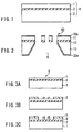
- FIG. 1 is a cross-sectional view showing a substrate (SOI substrate) for a transfer mask according to one example of the present invention.
- the substrate (SOI substrate) for a transfer mask 4 is constituted by a laminated structure comprising a lower monocrystalline silicon wafer 3 in which openings are to be subsequently formed, an upper monocrystalline silicon wafer 1 in which a transfer pattern is to be subsequently formed, and a silicon oxide film 2 interposed between the lower monocrystalline silicon wafer 3 and the upper monocrystalline silicon wafer 1.
- This laminated structure is featured in that the thickness of the silicon oxide film 2 is confined to a range of 0.2 ⁇ m to 0.8 ⁇ m.
- the etching resistance of the silicon oxide film 2 may become insufficient, thereby easily inviting a phenomenon wherein the etching is permitted to proceed passing through the silicon oxide film 2, because over-etching is usually performed taking the in-plane distribution of etching depth or the distribution of etching depth depending on the size of pattern into consideration on the occasion of performing dry etching of the upper monocrystalline silicon wafer 1.
- a wet etching liquid is permitted to penetrate through this etched through-hole formed in the silicon oxide film 2 on the occasion of wet etching to form an opening portion in the lower monocrystalline silicon wafer 3, thereby raising a problem that the transfer pattern formed on the upper monocrystalline silicon wafer 1 may be destroyed.
- an inert gas as a cooling medium is allowed to leak through this etched through-hole formed in the silicon oxide film 2 on the occasion of dry etching to form an opening portion in the lower monocrystalline silicon wafer 3 while directly cooling the substrate by making use of a cooling medium, thereby raising a problem that the discharging for etching is caused to be suspended in a midway of the etching process.
- This leakage of inert gas is also caused in the case where the etching of the lower monocrystalline silicon wafer 3 is performed prior to the formation of the transfer pattern.
- the thickness of the silicon oxide film 2 is larger than 0.8 ⁇ m, cracks may be generated in the transfer pattern, thereby destroying the transfer pattern due to the stress from the silicon oxide film 2 on the occasion where the silicon oxide film 2 is permitted to be expose due to wet etching or dry etching of the lower monocrystalline silicon wafer 3 to form an opening therein.
- the thickness of the silicon oxide film 2 is confined within the range of 0.2 ⁇ m to 0.8 ⁇ m, the phenomenon of generating cracks in the transfer pattern to destroy the transfer pattern can be prevented.
- a monocrystalline or polycrystalline silicon layer deposited on the surface of the silicon oxide film 2 may be substituted for the upper monocrystalline silicon wafer 1.
- the thickness of the upper monocrystalline silicon wafer or the upper silicon layer should preferably be within the range of 0.1 ⁇ m to 50 ⁇ m, more preferably, within the range of 1 ⁇ m to 50 ⁇ m.
- the thickness of the upper monocrystalline silicon wafer or the upper silicon layer should preferably be within the range of 0.1 to 3 ⁇ m.
- the thickness of the upper monocrystalline silicon wafer or the upper silicon layer should preferably be within the range of 5 to 50 ⁇ m.
- the upper monocrystalline silicon wafer or the upper silicon layer may be fused away as the magnitude of electric current is increased in order to enhance throughput.
- the thickness of the upper monocrystalline silicon wafer or the upper silicon layer is too thick, it may become difficult to form a transfer pattern.
- the thickness of the lower monocrystalline silicon wafer according to the present invention should preferably be within the range of about 400 ⁇ m to 1 mm. Because, if the thickness of the lower monocrystalline silicon wafer is less than 400 ⁇ m, it may be no longer possible to ensure its function as a supporting body for the transfer mask. On the other hand, if the thickness of the lower monocrystalline silicon wafer exceeds 1 mm, it may become difficult to satisfactorily work the substrate, i.e., the lower monocrystalline silicon wafer.
- FIG. 2 is a cross-sectional view showing one example of a transfer mask which was manufactured by making use of the aforementioned substrate (SOI substrate) 4 for a transfer mask, representing another embodiment of the present invention.
- the transfer mask 40 according to another embodiment of the present invention is constituted by a lower monocrystalline silicon wafer 13 having an opening 9, a silicon oxide film 12 having an opening, and an upper monocrystalline silicon wafer 11 bearing therein a transfer pattern 6.
- FIG. 2 represents one embodiment where a conductive film 20a is formed on the lower monocrystalline silicon wafer 13 having an opening 9, and at the same time, a conductive film 20b is formed on the upper monocrystalline silicon wafer 11 bearing therein a transfer pattern.
- these conductive films 20a, 20b are not necessarily essential, and may be omitted.
- a fine pattern is formed on the surface of the upper monocrystalline silicon wafer 11.
- This process of forming this fine pattern is performed by a sequence of steps comprising, stepwise, a step of forming a resist pattern on the surface of the upper monocrystalline silicon wafer 11, a step of dry-etching the upper monocrystalline silicon wafer 11 by making use of this resist pattern as a mask, and a step of removing the resist pattern.
- the exposure process of forming the resist pattern can be suitably performed by directly scanning an electron beam using a resist for an electron beam, or by means of stepper exposure using a photoresist.
- etching resistance of the resist is found insufficient on the occasion of dry-etching the upper monocrystalline silicon wafer, it is possible to employ, as an etching mask, an inorganic film such as a silicon oxide film, a silicon nitride film, a silicon carbide film, etc.; a metallic film made of chromium, tungsten, tantalum, titanium, nickel, aluminum, etc., or an alloy of these metals; or a metallic compound film formed through a reaction between any of these metals or alloys and oxygen, nitrogen, carbon, etc.
- etching masks can be formed by means of various kinds of thin film-forming method. For example, it is possible to employ a sputtering method, a CVD method, a vapor deposition method, etc.
- the dry etching method there is not any particular limitation with respect to the conditions for the etching.
- the gas to be employed in the dry etching it is possible to employ a mixed gas mainly comprising a fluorine-containing gas such as SF 6 gas and CF 4 gas.; a mixed gas mainly comprising a chlorine-containing gas such as Cl 2 gas and SiCl 4 gas; or a mixed gas mainly comprising a bromine-containing gas such as HBr gas.
- the dry etching apparatus it is possible to employ that where RIE, magnetron RIE, ECR, ICP, microwaves, helicon waves, NLD, etc., is employed as a discharge system.
- openings are formed in the lower monocrystalline silicon wafer, wherein dry etching, wet etching, ultrasonic working, sand blasting, etc., can be suitably employed.
- the step of forming a transfer pattern in the upper monocrystalline silicon wafer may be performed prior to or subsequent to the step of forming openings in the lower monocrystalline silicon wafer.
- the silicon oxide film formed on the openings is removed.
- the silicon oxide film can be removed by making use of hydrofluoric acid, which is followed by the formation of conductive film on opposite main surfaces if required, thereby accomplishing a transfer mask.
- the conductive film it is possible to employ a metal such as gold, platinum, palladium, tantalum, tungsten, molybdenum and osmium; or an alloy containing any of these metals. These metals can be employed singly or together with an underlying layer.
- the method of forming the conductive film it is possible to employ a sputtering method, a CVD method, a vapor deposition method, a plating method, an electrode position method, an ion plating method, etc.
- the formation of openings in the lower monocrystalline silicon wafer can be performed prior to the formation of a transfer pattern in the upper monocrystalline silicon wafer.
- part of the silicon oxide film which is exposed through the openings formed in the lower monocrystalline silicon wafer may be selectively removed prior to the formation of a transfer pattern in the upper monocrystalline silicon wafer.
- the transfer pattern is cracked or destroyed due to stress generated in the silicon oxide film, since the silicon oxide film does not exist at this portion.
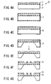
- FIGS. 3A to 3I are cross-sectional views illustrating stepwise one example of a manufacturing process of a transfer mask by making use of a substrate for a transfer mask according to one embodiment of the present invention.
- an SOI substrate exhibiting a plane orientation of (100) was employed as a substrate 4 for a transfer mask (which is referred to also as a transfer mask substrate).
- This transfer mask substrate 4 was constituted by a laminated structure comprising an upper monocrystalline silicon wafer 1, a lower monocrystalline silicon wafer 3, and a silicon oxide film 2 interposed between these upper monocrystalline silicon wafer 1 and lower monocrystalline silicon wafer 3.
- the thickness of the upper monocrystalline silicon wafer 1 was 20 ⁇ m
- the thickness of the silicon oxide film was 0.5 ⁇ m
- the thickness of the lower monocrystalline silicon wafer 3 was 500 ⁇ m.
- a resist for an electron beam (ZEP520, Nihon Zeon Co., Ltd.) was coated to a thickness of 0.5 ⁇ m on the surface of the upper monocrystalline silicon wafer 1 of the transfer mask substrate 4, and a pattern was described on the resist by making use of an electron beam drawing machine exhibiting an accelerating voltage of 50 kV.
- a developing solution for exclusive use ZED-N50, Nihon Zeon Co., Ltd.
- the dry etching of the upper monocrystalline silicon wafer 1 was performed to a depth extending to the silicon oxide film 2 by means of an ICP (inductively coupled plasma) dry etching apparatus, thereby forming a transfer pattern 6 as shown in FIG. 3C.
- ICP inductively coupled plasma
- a silicon nitride film 7 having a thickness of 0.3 ⁇ m was formed on the opposite main surfaces and peripheral wall of the transfer mask substrate as shown in FIG. 3D by means of an LPCVD (Low Pressure Chemical Vapor Deposition) apparatus.
- LPCVD Low Pressure Chemical Vapor Deposition
- the silicon nitride film formed on the surface of the lower monocrystalline silicon wafer was subjected to dry etching by making use of a mixed gas mainly containing CHF 3 gas and by means of an RIE (Reactive Ion Etching) apparatus, thereby forming a protective pattern 8 for wet etching as shown in FIG. 3E.
- RIE Reactive Ion Etching
- the substrate bearing thereon the protective pattern 8 was set on a jig so as to protect the transfer pattern formed on the upper monocrystalline silicon wafer, and was immersed in an etching solution consisting of an aqueous solution of KOH which was heated to a temperature of about 90°C.
- the etching was performed using the protective pattern 8 as a mask to such an extent that the anisotropic etching of the lower monocrystalline silicon wafer 3 along the plane orientation thereof proceeded down to the silicon oxide film 2 functioning as an etching stopper, thereby forming an opening 9 as shown in FIG. 3F.
- the reference number 3' in FIG. 3F represents the lower monocrystalline silicon wafer in which the opening 9 was formed.
- the protective pattern 8 was etched away by making use of hot phosphoric acid heated to about 170°C. Thereafter, as shown in FIG. 3H, the exposed portion of the silicon oxide film 2 was etched away by making use of hydrofluoric acid.
- the reference number 2' in FIG. 3G represents the silicon oxide film in which openings were formed.
- a platinum-palladium alloy having a thickness of about 0.1 ⁇ m was deposited on the opposite main surfaces of the resultant body by means of a magnetron sputtering apparatus to thereby form conductive films 10a and 10b, thus accomplishing a transfer mask as shown in FIG. 3I.
- the transfer mask manufactured in this manner was free from cracks of the upper monocrystalline silicon wafer that might be caused by stress from the silicon oxide film, thereby obtaining a transfer mask which was excellent in quality.
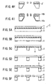
- FIGS. 4A to 4I are cross-sectional views illustrating stepwise another example of a manufacturing process of a transfer mask by making use of a transfer mask substrate according to another embodiment of the present invention.
- an SOI substrate exhibiting a plane orientation of (100) was employed as a substrate 4 for a transfer mask (which is referred to also as a transfer mask substrate).
- This transfer mask substrate 4 was constituted by a laminate structure having the same constituent components as described in Example 1.
- the thickness of the upper monocrystalline silicon wafer 1 was 20 ⁇ m
- the thickness of the silicon oxide film was 0.5 ⁇ m
- the thickness of the lower monocrystalline silicon wafer 3 was 500 ⁇ m.
- a silicon nitride film 7 was formed all over the transfer mask substrate 4 including the opposite main surfaces and peripheral wall thereof by means of the CVD method, and then, the silicon nitride film formed on the surface of the lower monocrystalline silicon wafer 3 was subjected to a patterning treatment, thereby forming a protective pattern 8 for wet etching as shown in FIG. 4C.
- the lower monocrystalline silicon wafer 3 having thereon the protective pattern 8 was set on a jig and immersed in an etching solution consisting of an aqueous solution of KOH which was heated to a temperature of about 90°C.
- the etching was performed using the protective pattern 8 as a mask to such an extent that the anisotropic etching of the lower monocrystalline silicon wafer 3 along the plane orientation thereof proceeded down to the silicon oxide film 2 functioning as an etching stopper, thereby forming an opening 9 as shown in FIG. 4D.
- the reference number 3' in FIG. 4D represents the lower monocrystalline silicon wafer in which the opening 9 was formed.
- the protective pattern 8 was etched away by making use of hot phosphoric acid heated to about 170°C. Thereafter, a resist for an electron beam was coated to a thickness of 0.5 ⁇ m on the surface of the upper monocrystalline silicon wafer 1, and a pattern was described on the resist by making use of an electron beam drawing machine exhibiting an accelerating voltage of 50 kV. Subsequently, by making use of a developing solution for exclusive use, the development of the resist was performed, thereby forming a resist pattern 5 as shown in FIG. 4F.
- the resist for an electron beam and the developing solution both employed herein were the same as those employed in Example 1.
- the dry etching of the upper monocrystalline silicon wafer 1 was performed to a depth extending to the silicon oxide film 2 by means of an ICP (inductively coupled plasma) dry etching apparatus, thereby forming a transfer pattern 6 as shown in FIG. 4G.
- ICP inductively coupled plasma
- the resist pattern 5 was removed as shown in FIG. 4H, and at the same time, the exposed portion of the silicon oxide film 2 was etched away by making use of buffer hydrofluoric acid.
- the reference number 2' in FIG. 4H represents the silicon oxide film in which openings were formed.
- tantalum having a thickness of about 0.1 ⁇ m was deposited on the opposite main surfaces of the resultant body by means of an electron beam vapor deposition apparatus to thereby form conductive films 10a and 10b, thus accomplishing a transfer mask.
- the transfer mask manufactured in this manner was free from cracks of the upper monocrystalline silicon wafer that might be caused by stress from the silicon oxide film, thereby obtaining a transfer mask which was excellent in quality.
- FIGS. 5A to 5F are cross-sectional views illustrating stepwise a further example of a manufacturing process of a transfer mask by making use of a transfer mask substrate according to a further embodiment of the present invention.
- an SOI substrate exhibiting a plane orientation of (100) was employed as a substrate for a transfer mask 4.
- This transfer mask substrate 4 was constituted by a laminate structure having the same constituent components as described in Example 1.
- the thickness of the upper monocrystalline silicon wafer 1 was 2 ⁇ m
- the thickness of the silicon oxide film was 0.7 ⁇ m
- the thickness of the lower monocrystalline silicon wafer 3 was 500 ⁇ m.
- a resist pattern 5 was formed on the surface of a lower monocrystalline silicon wafer 3 by means of ordinary photolithography. Subsequently, by making use of this resist pattern 5 as a mask together with the employment of a mixed gas mainly consisting of SF 6 as an etchant, etching of the lower monocrystalline silicon wafer 3 was performed by means of an ICP (inductively coupled plasma) dry etching apparatus to thereby form openings 9 as shown in FIG. 5C.
- ICP inductively coupled plasma
- the silicon oxide film 2 having a thickness of 0.7 ⁇ m was sufficiently capable of acting as an etching stopper. Further, the cross-section of the lower monocrystalline silicon wafer 3' which was provided with openings as a result of the aforementioned etching was found as having substantially perpendicular sidewalls.
- the resist pattern 5 was removed by an ashing treatment using oxygen plasma, and the portion of the silicon oxide film 2 which was exposed through the openings 9 was completely etched away by making use of buffer hydrofluoric acid.
- the reference number 2' in FIG. 5D represents the silicon oxide film in which openings were formed.
- a resist for an electron beam was coated to a thickness of 1.0 ⁇ m on the surface of the upper monocrystalline silicon wafer 1, and a pattern was described on the resist by making use of an electron beam drawing machine exhibiting an accelerating voltage of 100 kV. Subsequently, by making use of a developing solution for exclusive use, the development of the resist was performed, thereby forming a resist pattern 5 as shown in FIG. 5E.
- the dry etching of the upper monocrystalline silicon wafer 1 was performed by means of an ICP (inductively coupled plasma) dry etching apparatus, thereby forming a transfer pattern 6 enabling the charged particle beam to pass therethrough.
- the resist pattern 5 was removed by making use of an organic solvent. As a result, as shown in FIG. 5F, a transfer mask having the transfer pattern 6 was accomplished.
- the transfer mask manufactured in this manner was mounted on a charged particle beam exposure apparatus, and this specimen was subjected to an exposure process using an electron beam as a charged particle beam.
- the electron beam emitted from an electron gun was irradiated onto the transfer mask mounted on the stage arranged at a predetermined position in such a manner as to shape the charged particle beam in conformity with the configuration of the transfer pattern, the resultant shaped pattern of the charged particle beam being subsequently reduced by means of an electron lens and image-formed on the surface of the specimen having the resist film.
- an exposure of high precision which was exactly the same as designed.
- a transfer mask was manufactured under the same conditions as those of Example 1 except that the thickness of the silicon oxide film was set to 0.1 ⁇ m.
- the thickness of the silicon oxide film was set to 0.1 ⁇ m.
- a transfer mask was manufactured under the same conditions as those of Example 1 except that the thickness of the silicon oxide film was set to 1 ⁇ m.
- the upper monocrystalline silicon wafer of the transfer mask thus manufactured was investigated through observation thereof, cracking of the upper monocrystalline silicon wafer due to stress by the silicon oxide film was recognized, and hence the yield of the transfer mask which was free from cracking was found to be 0%.
- the transfer mask substrate which is constituted by a laminated structure comprising two silicon layers, and a silicon oxide film interposed between this pair of silicon layers is constructed such that the thickness of silicon oxide film was confined within the range of 0.2 ⁇ m to 0.8 ⁇ m, it is possible to attain the effect that the transfer pattern formed on the upper monocrystalline silicon wafer is caused to fracture due to stress by the silicon oxide film.
- the transfer mask manufactured by making use of the aforementioned transfer mask substrate is of such a high quality that the upper monocrystalline silicon wafer can hardly be destroyed.
Landscapes
- Physics & Mathematics (AREA)
- General Physics & Mathematics (AREA)
- Health & Medical Sciences (AREA)
- Toxicology (AREA)
- Preparing Plates And Mask In Photomechanical Process (AREA)
- Electron Beam Exposure (AREA)
Abstract
A substrate for a transfer mask, which comprises
a first silicon layer formed of monocrystalline
silicon, a silicon oxide film formed on the first
silicon layer and having a thickness ranging from 0.2
to 0.8 µm, and a second silicon layer formed on the
silicon oxide film. A transfer mask which is
manufactured by making use of this substrate is
featured in that it is possible to prevent a transfer
pattern from being cracked or destroyed due to stress
from the silicon oxide film on the occasion of
manufacturing the transfer mask, thereby providing
a defect-free transfer mask.
Description
The present invention relates to a substrate for
a transfer mask which is adapted for use in an exposure
process using a charged beam such as electron beam
or ion beam. The present invention relates also to
a transfer mask and to the manufacturing method of
the transfer mask.
Recently, electron beam lithography, ion beam
lithography, etc., where an electron beam or ion beam
is employed as an exposure light source, have come to
be seen as useful in a technique for manufacturing
elements having an ultrafine pattern of the next
generation. In the exposure process utilizing these
manufacturing techniques, it is required to employ
a transfer mask. In the manufacture of this transfer
mask, a substrate formed of an SOI (Silicon On
Insulator) substrate is employed because of the
easiness in fine working.
This SOI substrate for forming a transfer pattern
is constituted by a lower monocrystalline silicon wafer
as a substrate, a silicon oxide film formed on the
lower monocrystalline silicon wafer and functioning
as an etching stopper, and an upper monocrystalline
silicon wafer formed on the silicon oxide film,
the transfer pattern being formed on the upper
monocrystalline silicon wafer.
The thickness of silicon oxide film constituting
part of the SOI substrate to be employed as a substrate
for a transfer mask is generally within the range of
about 1 µm to 2 µm. However, there is a problem in
the employment of the SOI substrate comprising a
silicon oxide film having such a magnitude of thickness
that cracks tend to be formed in the upper
monocrystalline silicon wafer due to stress imposed
thereon by the silicon oxide film, thereby destroying
the transfer pattern and hence deteriorating the
manufacturing efficiency of the transfer mask.
Therefore, an object of the present invention is
to provide a substrate for a transfer mask, which
comprises a couple of silicon layers laminated with
a silicon oxide film being interposed therebetween,
and which makes it possible to stably manufacture
a defect-free transfer mask, i.e. a transfer mask
wherein a transfer pattern formed on the upper silicon
layer is prevented from being destroyed due to stress
from the silicon oxide film on the occasion of
manufacturing a transfer mask by making use of the
substrate.
Another object of the present invention is to
provide a transfer mask which comprises a transfer
pattern formed on the upper silicon layer of the
aforementioned substrate for a transfer mask, and which
makes it possible to prevent the transfer pattern
formed on the upper silicon layer from being destroyed
due to stress from the silicon oxide film on the
occasion of manufacturing the transfer mask, thereby
providing a defect-free transfer mask.
A further object of the present invention is to
provide a method of manufacturing the aforementioned
transfer mask, which makes it possible to prevent the
transfer pattern formed on the upper silicon layer from
being destroyed due to stress from the silicon oxide
film, thereby enabling a defect-free transfer mask to
be manufactured.
According to the present invention, there is
provided a substrate for a transfer mask, which
comprises a first silicon layer formed of
monocrystalline silicon; a silicon oxide film formed on
the first silicon layer and having a thickness ranging
from 0.2 to 0.8 µm; and a second silicon layer formed
on the silicon oxide film.
According to the present invention, there is
further provided a transfer mask comprising a first
silicon layer formed of monocrystalline silicon;
a silicon oxide film formed on the first silicon layer
and having a thickness ranging from 0.2 to 0.8 µm;
and a second silicon layer formed on the silicon oxide
film and bearing therein a transfer pattern; wherein
openings are formed in the first silicon layer, and
the portions of the silicon oxide film which correspond
to the openings are removed.
According to the present invention, there is
further provided a method of manufacturing a transfer
mask, the method comprising: preparing a substrate
comprising a first silicon layer formed of
monocrystalline silicon, a silicon oxide film formed on
the first silicon layer and having a thickness ranging
from 0.2 to 0.8 µm, and a second silicon layer formed
on the silicon oxide film; forming a transfer pattern
on the second silicon layer; forming openings in the
first silicon layer before or after forming the
transfer pattern; and selectively removing portions of
the silicon oxide film which correspond to the
openings.
According to the present invention, there is
further provided a method of manufacturing a transfer
mask, the method comprising: preparing a substrate
comprising a first silicon layer formed of
monocrystalline silicon, a silicon oxide film formed on
the first silicon layer and having a thickness ranging
from 0.2 to 0.8 µm, and a second silicon layer formed
on the silicon oxide film; forming openings in the
first silicon layer; selectively removing portions
of the silicon oxide film which correspond to the
openings; and forming a transfer pattern in the second
silicon layer.
According to the present invention, there is
further provided a method of irradiating a charged
particle beam, the method comprising: irradiating a
charged particle beam onto the aforementioned transfer
mask in such a manner as to shape the charged particle
beam in conformity with the configuration of a transfer
pattern; and image-forming a pattern of the shaped
charged particle beam on a substrate through a lens.
It is preferable in the present invention that the
second silicon layer has a film thickness of 0.1 to
50 µm. Further, the second silicon layer should
preferably be formed of monocrystalline silicon.
The substrate for a transfer mask according to the
present invention should preferably be formed of an SOI
substrate comprising two monocrystalline silicon wafers
superposed on one another via a silicon oxide film
being interposed therebetween.
Next, a substrate for a transfer mask as well as
a transfer mask according to one embodiment of the
present invention will be explained in detail with
reference to the drawings.
FIG. 1 is a cross-sectional view showing a
substrate (SOI substrate) for a transfer mask according
to one example of the present invention. Referring to
FIG. 1, the substrate (SOI substrate) for a transfer
mask 4 is constituted by a laminated structure
comprising a lower monocrystalline silicon wafer 3
in which openings are to be subsequently formed,
an upper monocrystalline silicon wafer 1 in which
a transfer pattern is to be subsequently formed, and
a silicon oxide film 2 interposed between the lower
monocrystalline silicon wafer 3 and the upper
monocrystalline silicon wafer 1. This laminated
structure is featured in that the thickness of the
silicon oxide film 2 is confined to a range of 0.2 µm
to 0.8 µm.
If the thickness of the silicon oxide film 2 is
less than 0.2 µm, the etching resistance of the
silicon oxide film 2 may become insufficient, thereby
easily inviting a phenomenon wherein the etching is
permitted to proceed passing through the silicon oxide
film 2, because over-etching is usually performed
taking the in-plane distribution of etching depth or
the distribution of etching depth depending on the size
of pattern into consideration on the occasion of
performing dry etching of the upper monocrystalline
silicon wafer 1.
When the etching is permitted to proceed passing
through the silicon oxide film 2, a wet etching liquid
is permitted to penetrate through this etched through-hole
formed in the silicon oxide film 2 on the occasion
of wet etching to form an opening portion in the lower
monocrystalline silicon wafer 3, thereby raising a
problem that the transfer pattern formed on the upper
monocrystalline silicon wafer 1 may be destroyed.
Further, when the etching is permitted to proceed
passing through the silicon oxide film 2, an inert gas
as a cooling medium is allowed to leak through this
etched through-hole formed in the silicon oxide film 2
on the occasion of dry etching to form an opening
portion in the lower monocrystalline silicon wafer 3
while directly cooling the substrate by making use of
a cooling medium, thereby raising a problem that the
discharging for etching is caused to be suspended in
a midway of the etching process. This leakage of inert
gas is also caused in the case where the etching of the
lower monocrystalline silicon wafer 3 is performed
prior to the formation of the transfer pattern.
On the other hand, if the thickness of the silicon
oxide film 2 is larger than 0.8 µm, cracks may be
generated in the transfer pattern, thereby destroying
the transfer pattern due to the stress from the silicon
oxide film 2 on the occasion where the silicon oxide
film 2 is permitted to be expose due to wet etching or
dry etching of the lower monocrystalline silicon wafer
3 to form an opening therein.
Namely, when the thickness of the silicon oxide
film 2 is confined within the range of 0.2 µm to
0.8 µm, the phenomenon of generating cracks in the
transfer pattern to destroy the transfer pattern can be
prevented.
Incidentally the way, a monocrystalline or
polycrystalline silicon layer deposited on the surface
of the silicon oxide film 2 may be substituted for the
upper monocrystalline silicon wafer 1.
Further, in the present invention, the thickness
of the upper monocrystalline silicon wafer or the upper
silicon layer should preferably be within the range of
0.1 µm to 50 µm, more preferably, within the range of
1 µm to 50 µm.
If the transfer mask of the present invention is
to be applied to a scattering type transfer mask, the
thickness of the upper monocrystalline silicon wafer
or the upper silicon layer should preferably be within
the range of 0.1 to 3 µm. Whereas, if the transfer
mask of the present invention is to be applied to
a shielding type transfer mask, the thickness of
the upper monocrystalline silicon wafer or the upper
silicon layer should preferably be within the range of
5 to 50 µm.
In either case, if the thickness of the upper
monocrystalline silicon wafer or the upper silicon
layer is too thin, the upper monocrystalline silicon
wafer or the upper silicon layer may be fused away as
the magnitude of electric current is increased in order
to enhance throughput. On the other hand, if the
thickness of the upper monocrystalline silicon wafer or
the upper silicon layer is too thick, it may become
difficult to form a transfer pattern.
Further, the thickness of the lower
monocrystalline silicon wafer according to the present
invention should preferably be within the range of
about 400 µm to 1 mm. Because, if the thickness of
the lower monocrystalline silicon wafer is less than
400 µm, it may be no longer possible to ensure its
function as a supporting body for the transfer mask.
On the other hand, if the thickness of the lower
monocrystalline silicon wafer exceeds 1 mm, it may
become difficult to satisfactorily work the substrate,
i.e., the lower monocrystalline silicon wafer.
FIG. 2 is a cross-sectional view showing one
example of a transfer mask which was manufactured by
making use of the aforementioned substrate (SOI
substrate) 4 for a transfer mask, representing another
embodiment of the present invention. As shown in
FIG. 2, the transfer mask 40 according to another
embodiment of the present invention is constituted by
a lower monocrystalline silicon wafer 13 having an
opening 9, a silicon oxide film 12 having an opening,
and an upper monocrystalline silicon wafer 11 bearing
therein a transfer pattern 6.
The construction shown in FIG. 2 represents one
embodiment where a conductive film 20a is formed on
the lower monocrystalline silicon wafer 13 having an
opening 9, and at the same time, a conductive film 20b
is formed on the upper monocrystalline silicon wafer 11
bearing therein a transfer pattern. However, these
conductive films 20a, 20b are not necessarily
essential, and may be omitted.
Next, the manufacturing process of the transfer
mask according to another embodiment of the present
invention will be explained as follows.
First of all, a fine pattern is formed on the
surface of the upper monocrystalline silicon wafer 11.
This process of forming this fine pattern is performed
by a sequence of steps comprising, stepwise, a step of
forming a resist pattern on the surface of the upper
monocrystalline silicon wafer 11, a step of dry-etching
the upper monocrystalline silicon wafer 11 by making
use of this resist pattern as a mask, and a step of
removing the resist pattern.
The exposure process of forming the resist pattern
can be suitably performed by directly scanning an
electron beam using a resist for an electron beam, or
by means of stepper exposure using a photoresist.
In the case where the etching resistance of the
resist is found insufficient on the occasion of dry-etching
the upper monocrystalline silicon wafer, it is
possible to employ, as an etching mask, an inorganic
film such as a silicon oxide film, a silicon nitride
film, a silicon carbide film, etc.; a metallic film
made of chromium, tungsten, tantalum, titanium, nickel,
aluminum, etc., or an alloy of these metals; or
a metallic compound film formed through a reaction
between any of these metals or alloys and oxygen,
nitrogen, carbon, etc. These etching masks can be
formed by means of various kinds of thin film-forming
method. For example, it is possible to employ a
sputtering method, a CVD method, a vapor deposition
method, etc.
As for the dry etching method, there is not any
particular limitation with respect to the conditions
for the etching. As for the gas to be employed in
the dry etching, it is possible to employ a mixed gas
mainly comprising a fluorine-containing gas such as SF6
gas and CF4 gas.; a mixed gas mainly comprising a
chlorine-containing gas such as Cl2 gas and SiCl4 gas;
or a mixed gas mainly comprising a bromine-containing
gas such as HBr gas. As for the dry etching apparatus,
it is possible to employ that where RIE, magnetron RIE,
ECR, ICP, microwaves, helicon waves, NLD, etc., is
employed as a discharge system.
Next, openings are formed in the lower
monocrystalline silicon wafer, wherein dry etching,
wet etching, ultrasonic working, sand blasting, etc.,
can be suitably employed.
Incidentally, the step of forming a transfer
pattern in the upper monocrystalline silicon wafer may
be performed prior to or subsequent to the step of
forming openings in the lower monocrystalline silicon
wafer.
Next, the silicon oxide film formed on the
openings is removed. Specifically, the silicon oxide
film can be removed by making use of hydrofluoric acid,
which is followed by the formation of conductive
film on opposite main surfaces if required, thereby
accomplishing a transfer mask.
As for the conductive film, it is possible to
employ a metal such as gold, platinum, palladium,
tantalum, tungsten, molybdenum and osmium; or an alloy
containing any of these metals. These metals can be
employed singly or together with an underlying layer.
As for the method of forming the conductive film, it is
possible to employ a sputtering method, a CVD method,
a vapor deposition method, a plating method, an
electrode position method, an ion plating method, etc.
As described above, the formation of openings
in the lower monocrystalline silicon wafer can be
performed prior to the formation of a transfer
pattern in the upper monocrystalline silicon wafer.
In this case, part of the silicon oxide film which is
exposed through the openings formed in the lower
monocrystalline silicon wafer may be selectively
removed prior to the formation of a transfer pattern
in the upper monocrystalline silicon wafer. On the
occasion of forming a transfer pattern in this process,
there is little possibility that the transfer pattern
is cracked or destroyed due to stress generated in the
silicon oxide film, since the silicon oxide film does
not exist at this portion.
However, in order to prevent leakage of the inert
gas to be employed for cooling the substrate on the
occasion of the dry etching step for forming a transfer
pattern on the upper monocrystalline silicon wafer,
it may be necessary to take some sort of measures such
as the placement of the lower monocrystalline silicon
wafer on a holder which is excellent in thermal
conductivity.
Next, specific example of the present invention
will be explained with reference to drawings.
FIGS. 3A to 3I are cross-sectional views
illustrating stepwise one example of a manufacturing
process of a transfer mask by making use of a substrate
for a transfer mask according to one embodiment of the
present invention. First of all, as shown in FIG. 3A,
an SOI substrate exhibiting a plane orientation of
(100) was employed as a substrate 4 for a transfer
mask (which is referred to also as a transfer mask
substrate). This transfer mask substrate 4 was
constituted by a laminated structure comprising
an upper monocrystalline silicon wafer 1, a lower
monocrystalline silicon wafer 3, and a silicon oxide
film 2 interposed between these upper monocrystalline
silicon wafer 1 and lower monocrystalline silicon wafer
3. The thickness of the upper monocrystalline silicon
wafer 1 was 20 µm, the thickness of the silicon oxide
film was 0.5 µm, and the thickness of the lower
monocrystalline silicon wafer 3 was 500 µm.
Then, a resist for an electron beam (ZEP520, Nihon
Zeon Co., Ltd.) was coated to a thickness of 0.5 µm on
the surface of the upper monocrystalline silicon wafer
1 of the transfer mask substrate 4, and a pattern was
described on the resist by making use of an electron
beam drawing machine exhibiting an accelerating voltage
of 50 kV. Subsequently, by making use of a developing
solution for exclusive use (ZED-N50, Nihon Zeon Co.,
Ltd.), the development of the resist was performed,
thereby forming a resist pattern 5 as shown in FIG. 3B.
Next, by making use of the resist pattern 5 as a
mask together with the employment of a mixed gas mainly
consisting of fluorine-containing gas, i.e., SF6, as an
etchant, the dry etching of the upper monocrystalline
silicon wafer 1 was performed to a depth extending
to the silicon oxide film 2 by means of an ICP
(inductively coupled plasma) dry etching apparatus,
thereby forming a transfer pattern 6 as shown in
FIG. 3C.
Then, the resist pattern 5 was removed, and a
silicon nitride film 7 having a thickness of 0.3 µm
was formed on the opposite main surfaces and peripheral
wall of the transfer mask substrate as shown in FIG. 3D
by means of an LPCVD (Low Pressure Chemical Vapor
Deposition) apparatus.
Subsequently, the silicon nitride film formed on
the surface of the lower monocrystalline silicon wafer
was subjected to dry etching by making use of a mixed
gas mainly containing CHF3 gas and by means of an RIE
(Reactive Ion Etching) apparatus, thereby forming
a protective pattern 8 for wet etching as shown in
FIG. 3E.
Then, the substrate bearing thereon the protective
pattern 8 was set on a jig so as to protect the
transfer pattern formed on the upper monocrystalline
silicon wafer, and was immersed in an etching solution
consisting of an aqueous solution of KOH which was
heated to a temperature of about 90°C. Thus, the
etching was performed using the protective pattern 8 as
a mask to such an extent that the anisotropic etching
of the lower monocrystalline silicon wafer 3 along
the plane orientation thereof proceeded down to the
silicon oxide film 2 functioning as an etching stopper,
thereby forming an opening 9 as shown in FIG. 3F.
The reference number 3' in FIG. 3F represents the lower
monocrystalline silicon wafer in which the opening 9
was formed.
Next, as shown in FIG. 3G, the protective pattern
8 was etched away by making use of hot phosphoric
acid heated to about 170°C. Thereafter, as shown in
FIG. 3H, the exposed portion of the silicon oxide film
2 was etched away by making use of hydrofluoric acid.
The reference number 2' in FIG. 3G represents the
silicon oxide film in which openings were formed.
Finally, a platinum-palladium alloy having
a thickness of about 0.1 µm was deposited on the
opposite main surfaces of the resultant body by means
of a magnetron sputtering apparatus to thereby form
conductive films 10a and 10b, thus accomplishing
a transfer mask as shown in FIG. 3I.
The transfer mask manufactured in this manner was
free from cracks of the upper monocrystalline silicon
wafer that might be caused by stress from the silicon
oxide film, thereby obtaining a transfer mask which was
excellent in quality.
FIGS. 4A to 4I are cross-sectional views
illustrating stepwise another example of a manufacturing
process of a transfer mask by making use of
a transfer mask substrate according to another
embodiment of the present invention. First of all, as
shown in FIG. 4A, an SOI substrate exhibiting a plane
orientation of (100) was employed as a substrate 4 for
a transfer mask (which is referred to also as a
transfer mask substrate). This transfer mask substrate
4 was constituted by a laminate structure having the
same constituent components as described in Example 1.
The thickness of the upper monocrystalline silicon
wafer 1 was 20 µm, the thickness of the silicon oxide
film was 0.5 µm, and the thickness of the lower
monocrystalline silicon wafer 3 was 500 µm.
As shown in FIG. 4B, a silicon nitride film 7 was
formed all over the transfer mask substrate 4 including
the opposite main surfaces and peripheral wall thereof
by means of the CVD method, and then, the silicon
nitride film formed on the surface of the lower
monocrystalline silicon wafer 3 was subjected to
a patterning treatment, thereby forming a protective
pattern 8 for wet etching as shown in FIG. 4C.
Then, the lower monocrystalline silicon wafer 3
having thereon the protective pattern 8 was set on
a jig and immersed in an etching solution consisting
of an aqueous solution of KOH which was heated to
a temperature of about 90°C. Thus, the etching was
performed using the protective pattern 8 as a mask to
such an extent that the anisotropic etching of the
lower monocrystalline silicon wafer 3 along the plane
orientation thereof proceeded down to the silicon
oxide film 2 functioning as an etching stopper,
thereby forming an opening 9 as shown in FIG. 4D.
The reference number 3' in FIG. 4D represents
the lower monocrystalline silicon wafer in which the
opening 9 was formed.
Next, as shown in FIG. 4E, the protective pattern
8 was etched away by making use of hot phosphoric acid
heated to about 170°C. Thereafter, a resist for an
electron beam was coated to a thickness of 0.5 µm on
the surface of the upper monocrystalline silicon wafer
1, and a pattern was described on the resist by making
use of an electron beam drawing machine exhibiting
an accelerating voltage of 50 kV. Subsequently, by
making use of a developing solution for exclusive use,
the development of the resist was performed, thereby
forming a resist pattern 5 as shown in FIG. 4F. The
resist for an electron beam and the developing solution
both employed herein were the same as those employed in
Example 1.
Next, by making use of the resist pattern 5 as a
mask together with the employment of a mixed gas mainly
consisting of fluorine-containing gas, i.e., SF6, as an
etchant, the dry etching of the upper monocrystalline
silicon wafer 1 was performed to a depth extending
to the silicon oxide film 2 by means of an ICP
(inductively coupled plasma) dry etching apparatus,
thereby forming a transfer pattern 6 as shown in
FIG. 4G.
Then, the resist pattern 5 was removed as shown in
FIG. 4H, and at the same time, the exposed portion of
the silicon oxide film 2 was etched away by making use
of buffer hydrofluoric acid. The reference number 2'
in FIG. 4H represents the silicon oxide film in which
openings were formed.
Finally, as shown in FIG. 4I, tantalum having
a thickness of about 0.1 µm was deposited on the
opposite main surfaces of the resultant body by means
of an electron beam vapor deposition apparatus to
thereby form conductive films 10a and 10b, thus
accomplishing a transfer mask.
The transfer mask manufactured in this manner was
free from cracks of the upper monocrystalline silicon
wafer that might be caused by stress from the silicon
oxide film, thereby obtaining a transfer mask which was
excellent in quality.
FIGS. 5A to 5F are cross-sectional views
illustrating stepwise a further example of a manufacturing
process of a transfer mask by making use of
a transfer mask substrate according to a further
embodiment of the present invention. First of all, as
shown in FIG. 5A, an SOI substrate exhibiting a plane
orientation of (100) was employed as a substrate for
a transfer mask 4. This transfer mask substrate 4 was
constituted by a laminate structure having the same
constituent components as described in Example 1.
The thickness of the upper monocrystalline silicon
wafer 1 was 2 µm, the thickness of the silicon oxide
film was 0.7 µm, and the thickness of the lower
monocrystalline silicon wafer 3 was 500 µm.
Then, as shown in FIG. 5B, a resist pattern 5
was formed on the surface of a lower monocrystalline
silicon wafer 3 by means of ordinary photolithography.
Subsequently, by making use of this resist pattern 5
as a mask together with the employment of a mixed gas
mainly consisting of SF6 as an etchant, etching of the
lower monocrystalline silicon wafer 3 was performed
by means of an ICP (inductively coupled plasma) dry
etching apparatus to thereby form openings 9 as shown
in FIG. 5C.
When all of the portion of the lower
monocrystalline silicon wafer 3 for forming the
openings 9 was completely removed by way of etching,
the silicon oxide film 2 having a thickness of 0.7 µm
was sufficiently capable of acting as an etching
stopper. Further, the cross-section of the lower
monocrystalline silicon wafer 3' which was provided
with openings as a result of the aforementioned etching
was found as having substantially perpendicular
sidewalls.
Then, as shown in FIG. 5D, the resist pattern 5
was removed by an ashing treatment using oxygen plasma,
and the portion of the silicon oxide film 2 which was
exposed through the openings 9 was completely etched
away by making use of buffer hydrofluoric acid.
The reference number 2' in FIG. 5D represents the
silicon oxide film in which openings were formed.
Thereafter, a resist for an electron beam was
coated to a thickness of 1.0 µm on the surface of
the upper monocrystalline silicon wafer 1, and
a pattern was described on the resist by making use
of an electron beam drawing machine exhibiting
an accelerating voltage of 100 kV. Subsequently, by
making use of a developing solution for exclusive use,
the development of the resist was performed, thereby
forming a resist pattern 5 as shown in FIG. 5E.
Next, by making use of the resist pattern 5 as a
mask together with the employment of a mixed gas mainly
consisting of HBr as an etchant, the dry etching of
the upper monocrystalline silicon wafer 1 was performed
by means of an ICP (inductively coupled plasma) dry
etching apparatus, thereby forming a transfer pattern
6 enabling the charged particle beam to pass
therethrough. Subsequently, the resist pattern 5 was
removed by making use of an organic solvent. As a
result, as shown in FIG. 5F, a transfer mask having
the transfer pattern 6 was accomplished.
The transfer mask manufactured in this manner was
mounted on a charged particle beam exposure apparatus,
and this specimen was subjected to an exposure process
using an electron beam as a charged particle beam.
Namely, the electron beam emitted from an electron
gun was irradiated onto the transfer mask mounted on
the stage arranged at a predetermined position in such
a manner as to shape the charged particle beam in
conformity with the configuration of the transfer
pattern, the resultant shaped pattern of the charged
particle beam being subsequently reduced by means of
an electron lens and image-formed on the surface of the
specimen having the resist film. As a result, it was
found possible to perform an exposure of high precision
which was exactly the same as designed.
A transfer mask was manufactured under the same
conditions as those of Example 1 except that the
thickness of the silicon oxide film was set to 0.1 µm.
When the upper monocrystalline silicon wafer of the
transfer mask thus manufactured was investigated
through observation thereof, destruction of the
transfer pattern due to the wet etching solution was
recognized.
A transfer mask was manufactured under the same
conditions as those of Example 1 except that the
thickness of the silicon oxide film was set to 1 µm.
When the upper monocrystalline silicon wafer of the
transfer mask thus manufactured was investigated
through observation thereof, cracking of the upper
monocrystalline silicon wafer due to stress by the
silicon oxide film was recognized, and hence the yield
of the transfer mask which was free from cracking was
found to be 0%.
As explained above, according to the present
invention, since the transfer mask substrate which is
constituted by a laminated structure comprising two
silicon layers, and a silicon oxide film interposed
between this pair of silicon layers is constructed such
that the thickness of silicon oxide film was confined
within the range of 0.2 µm to 0.8 µm, it is possible
to attain the effect that the transfer pattern formed
on the upper monocrystalline silicon wafer is caused to
fracture due to stress by the silicon oxide film.
Furthermore, the transfer mask manufactured by
making use of the aforementioned transfer mask
substrate is of such a high quality that the upper
monocrystalline silicon wafer can hardly be destroyed.
Moreover, according to the manufacturing method of
the transfer mask by making use of the aforementioned
transfer mask substrate, it is possible to stably
manufacture a defect-free transfer mask.
Additionally, according to the method of
irradiating a charged particle beam where the
aforementioned transfer mask is employed, it is now
possible to perform, at high precision, the patterning
exposure of the resist formed on a substrate.
As a result, patterning such as the patterning of
a semiconductor can be performed with high yield.
Claims (13)
- A substrate for a transfer mask, which comprises a first silicon layer formed of monocrystalline silicon; a silicon oxide film formed on the first silicon layer and having a thickness ranging from 0.2 to 0.8 µm; and a second silicon layer formed on the silicon oxide film.
- The substrate for a transfer mask according to claim 1, wherein said second silicon layer has a thickness ranging from 0.1 to 50 µm.
- The substrate for a transfer mask according to claim 1, wherein said second silicon layer is formed of monocrystalline silicon.
- A transfer mask comprising a first silicon layer formed of monocrystalline silicon; a silicon oxide film formed on the first silicon layer and having a thickness ranging from 0.2 to 0.8 µm; and a second silicon layer formed on the silicon oxide film and bearing therein a transfer pattern;
wherein openings are formed in said first silicon layer, and the portions of said silicon oxide film which correspond to said openings are removed. - The transfer mask according to claim 4,
wherein said second silicon layer has a thickness ranging from 0.1 to 50 µm. - The transfer mask according to claim 4,
wherein said second silicon layer is formed of monocrystalline silicon. - A method of manufacturing a transfer mask, the method comprising:preparing a substrate comprising a first silicon layer formed of monocrystalline silicon, a silicon oxide film formed on the first silicon layer and having a thickness ranging from 0.2 to 0.8 µm, and a second silicon layer formed on the silicon oxide film;forming a transfer pattern on said second silicon layer;forming openings in said first silicon layer before or after forming said transfer pattern; andselectively removing portions of said silicon oxide film which correspond to said openings.
- The method according to claim 7, wherein said second silicon layer has a thickness ranging from 0.1 to 50 µm.
- The method according to claim 7, wherein said second silicon layer is formed of monocrystalline silicon.
- A method of manufacturing a transfer mask, the method comprising:preparing a substrate comprising a first silicon layer formed of monocrystalline silicon, a silicon oxide film formed on the first silicon layer and having a thickness ranging from 0.2 to 0.8 µm, and a second silicon layer formed on the silicon oxide film;forming openings in said first silicon layer;selectively removing portions of said silicon oxide film which correspond to said openings; andforming a transfer pattern in said second silicon layer.
- The method according to claim 10, wherein said second silicon layer has a thickness ranging from 0.1 to 50 µm.
- The method according to claim 10, wherein said second silicon layer is formed of monocrystalline silicon.
- A method of irradiating a charged particle beam, the method comprising:irradiating a charged particle beam onto the transfer mask as claimed in Claim 4 in such a manner as to shape said charged particle beam in conformity with the configuration of a transfer pattern; andimage-forming a pattern of said shaped charged particle beam on a substrate through a lens.
Applications Claiming Priority (5)
| Application Number | Priority Date | Filing Date | Title |
|---|---|---|---|
| JP2000154661 | 2000-05-25 | ||
| JP2000154661 | 2000-05-25 | ||
| JP2000374109A JP2002050570A (en) | 1999-12-08 | 2000-12-08 | Transfer mask substrate, transfer mask, transfer mask manufacturing method, charged particle beam exposure method, and charged particle beam exposure apparatus |
| JP2000374109 | 2000-12-08 | ||
| PCT/JP2001/003638 WO2001091167A1 (en) | 2000-05-25 | 2001-04-26 | Substrate for transfer mask, transfer mask, and method of manufacture thereof |
Publications (2)
| Publication Number | Publication Date |
|---|---|
| EP1223607A1 true EP1223607A1 (en) | 2002-07-17 |
| EP1223607A4 EP1223607A4 (en) | 2003-03-12 |
Family
ID=26592586
Family Applications (1)
| Application Number | Title | Priority Date | Filing Date |
|---|---|---|---|
| EP01925969A Withdrawn EP1223607A4 (en) | 2000-05-25 | 2001-04-26 | SUBSTRATE FOR TRANSFER MASK, TRANSFER MASK AND MANUFACTURING METHOD THEREOF |
Country Status (5)
| Country | Link |
|---|---|
| US (1) | US6638666B2 (en) |
| EP (1) | EP1223607A4 (en) |
| KR (1) | KR100770196B1 (en) |
| CN (1) | CN1196175C (en) |
| WO (1) | WO2001091167A1 (en) |
Families Citing this family (11)
| Publication number | Priority date | Publication date | Assignee | Title |
|---|---|---|---|---|
| US6923920B2 (en) * | 2002-08-14 | 2005-08-02 | Lam Research Corporation | Method and compositions for hardening photoresist in etching processes |
| KR100471153B1 (en) * | 2002-11-27 | 2005-03-10 | 삼성전기주식회사 | Method of manufacturing and grounding micro-electro mechanical systems device using silicon on insulator wafer |
| US20040224243A1 (en) * | 2003-05-08 | 2004-11-11 | Sony Corporation | Mask, mask blank, and methods of producing these |
| US20050100798A1 (en) * | 2003-10-15 | 2005-05-12 | Taiwan Semiconductor Manufacturing Company, Ltd. | Device and method for providing wavelength reduction with a photomask |
| US20060211210A1 (en) * | 2004-08-27 | 2006-09-21 | Rensselaer Polytechnic Institute | Material for selective deposition and etching |
| US7482277B2 (en) * | 2004-11-23 | 2009-01-27 | Massachusetts Institute Of Technology | Multilevel fabrication processing by functional regrouping of material deposition, lithography, and etching |
| KR101117826B1 (en) * | 2005-02-18 | 2012-06-05 | 호야 가부시키가이샤 | Light-transmitting object examining method, manufacturing method for light-transmitting substrate of mask blank, manufacturing method for mask blank, manufacturing method for light-expososure mask, manufacturing method for semiconductor device and manufacturing method for phase shift mask |
| JP5271601B2 (en) * | 2008-05-16 | 2013-08-21 | 株式会社ブリヂストン | Single crystal manufacturing apparatus and manufacturing method |
| DE102009023371A1 (en) * | 2009-05-29 | 2010-12-02 | Acandis Gmbh & Co. Kg | Method for producing a medical functional element with a self-supporting lattice structure |
| JP2012090252A (en) * | 2010-09-22 | 2012-05-10 | Nippon Dempa Kogyo Co Ltd | Method for manufacturing piezoelectric device, and piezoelectric device |
| JP6531729B2 (en) * | 2016-07-19 | 2019-06-19 | 株式会社Sumco | Method of evaluating carbon concentration of silicon sample, method of evaluating silicon wafer manufacturing process, method of manufacturing silicon wafer, and method of manufacturing silicon single crystal ingot |
Family Cites Families (16)
| Publication number | Priority date | Publication date | Assignee | Title |
|---|---|---|---|---|
| JPS5789221A (en) | 1980-11-25 | 1982-06-03 | Seiko Epson Corp | Multiple mask |
| DE3524196C3 (en) | 1984-07-06 | 1994-08-04 | Canon Kk | Lithography mask |
| EP0424375B1 (en) | 1987-10-09 | 1993-10-13 | Hughes Aircraft Company | Monolithic channeling mask having amorphous/single crystal construction |
| JP2725319B2 (en) | 1988-11-07 | 1998-03-11 | 富士通株式会社 | Manufacturing method of charged particle beam mask |
| JP2506019B2 (en) * | 1991-04-25 | 1996-06-12 | 富士通株式会社 | Transmission mask manufacturing method |
| JP3060693B2 (en) | 1992-02-07 | 2000-07-10 | 松下電器産業株式会社 | Stencil mask forming method |
| JP3622308B2 (en) | 1996-01-04 | 2005-02-23 | 凸版印刷株式会社 | Transmission mask for batch exposure of charged beams |
| JP2904145B2 (en) | 1996-09-04 | 1999-06-14 | 日本電気株式会社 | Aperture for charged beam writing apparatus and method of manufacturing the same |
| JP2888211B2 (en) * | 1996-11-08 | 1999-05-10 | 日本電気株式会社 | Mask blank for electron beam exposure and method of manufacturing mask for electron beam exposure |
| DE19710799A1 (en) | 1997-03-17 | 1998-10-01 | Ibm | Membrane mask for exposure processes with short-wave radiation |
| JP3950628B2 (en) | 1998-03-25 | 2007-08-01 | インスティトゥート フュア ミクロエレクトロニク シュツットガルト スティフツング デス エッフェントリッヘン レヒツ | Method for manufacturing a broad membrane mask |
| JP3246445B2 (en) | 1998-07-01 | 2002-01-15 | 日本電気株式会社 | Transmission mask for charged beam batch exposure and method of manufacturing the same |
| US6124063A (en) * | 1998-07-30 | 2000-09-26 | Motorola, Inc. | Method of forming a semiconductor device utilizing lithographic mask and mask therefor |
| GB2351567A (en) | 1999-04-19 | 2001-01-03 | Ims Ionen Mikrofab Syst | Transmission mask and mask-exposure arrangement for projection lithography |
| JP2000306832A (en) * | 1999-04-19 | 2000-11-02 | Ims Ionen Mikrofab Syst Gmbh | Transmission mask and mask exposure system for projection lithography system |
| JP2000349023A (en) * | 1999-05-21 | 2000-12-15 | Ims Ionen Mikrofab Syst Gmbh | Transmission mask and mask exposure system for projection lithography system |
-
2001
- 2001-04-26 EP EP01925969A patent/EP1223607A4/en not_active Withdrawn
- 2001-04-26 KR KR1020027000954A patent/KR100770196B1/en not_active Expired - Fee Related
- 2001-04-26 WO PCT/JP2001/003638 patent/WO2001091167A1/en not_active Ceased
- 2001-04-26 CN CNB018014437A patent/CN1196175C/en not_active Expired - Fee Related
-
2002
- 2002-01-23 US US10/052,509 patent/US6638666B2/en not_active Expired - Fee Related
Also Published As
| Publication number | Publication date |
|---|---|
| CN1381068A (en) | 2002-11-20 |
| KR20020060686A (en) | 2002-07-18 |
| KR100770196B1 (en) | 2007-10-26 |
| US20020060297A1 (en) | 2002-05-23 |
| US6638666B2 (en) | 2003-10-28 |
| CN1196175C (en) | 2005-04-06 |
| EP1223607A4 (en) | 2003-03-12 |
| WO2001091167A1 (en) | 2001-11-29 |
Similar Documents
| Publication | Publication Date | Title |
|---|---|---|
| US6638666B2 (en) | Substrate for a transfer mask, transfer mask, and method of manufacturing the transfer mask | |
| JPH09213620A (en) | Transfer mask manufacturing method | |
| JP2988455B2 (en) | Plasma etching method | |
| JP2944559B2 (en) | Method for manufacturing through-hole for beam current measurement | |
| US6193870B1 (en) | Use of a hard mask for formation of gate and dielectric via nanofilament field emission devices | |
| JP2004200223A (en) | Mask blanks for charged particle beam exposure, mask blanks for charged particle beam exposure, and method of manufacturing mask | |
| JPWO2003017343A1 (en) | Dry development method | |
| JP4686914B2 (en) | Manufacturing method of stencil mask | |
| JPS6022340A (en) | Semiconductor device and manufacture of the same | |
| JP4654811B2 (en) | Etching mask and dry etching method | |
| JP3809754B2 (en) | Method for manufacturing transfer mask | |
| JPH08297361A (en) | Transfer mask | |
| JP2899542B2 (en) | Method of manufacturing transfer mask | |
| JPH0778748A (en) | Aperture mask and manufacturing method thereof | |
| JP3271390B2 (en) | Transmission mask for charged beam exposure and method of manufacturing the same | |
| JP3246849B2 (en) | Transfer mask | |
| JPH08254815A (en) | Transfer mask manufacturing method | |
| JP2002050570A (en) | Transfer mask substrate, transfer mask, transfer mask manufacturing method, charged particle beam exposure method, and charged particle beam exposure apparatus | |
| JP3143043B2 (en) | Transfer mask | |
| JPH05160078A (en) | Dry etching method | |
| JP2001267207A (en) | Electron beam exposure mask, method of manufacturing the same, and electron beam exposure apparatus | |
| JP2002151378A (en) | Transfer mask manufacturing method | |
| JP2001185481A (en) | Transfer mask | |
| JP2004311800A (en) | Mask blanks for charged particle beam exposure and method of manufacturing mask | |
| JP2006222154A (en) | Manufacturing method of semiconductor device |
Legal Events
| Date | Code | Title | Description |
|---|---|---|---|
| PUAI | Public reference made under article 153(3) epc to a published international application that has entered the european phase |
Free format text: ORIGINAL CODE: 0009012 |
|
| 17P | Request for examination filed |
Effective date: 20020424 |
|
| AK | Designated contracting states |
Kind code of ref document: A1 Designated state(s): AT BE CH CY DE DK ES FI FR GB GR IE IT LI LU MC NL PT SE TR |
|
| A4 | Supplementary search report drawn up and despatched |
Effective date: 20030124 |
|
| 17Q | First examination report despatched |
Effective date: 20090209 |
|
| STAA | Information on the status of an ep patent application or granted ep patent |
Free format text: STATUS: THE APPLICATION IS DEEMED TO BE WITHDRAWN |
|
| 18D | Application deemed to be withdrawn |
Effective date: 20100804 |