EP1220278A2 - Flat panel display device - Google Patents
Flat panel display device Download PDFInfo
- Publication number
- EP1220278A2 EP1220278A2 EP01130624A EP01130624A EP1220278A2 EP 1220278 A2 EP1220278 A2 EP 1220278A2 EP 01130624 A EP01130624 A EP 01130624A EP 01130624 A EP01130624 A EP 01130624A EP 1220278 A2 EP1220278 A2 EP 1220278A2
- Authority
- EP
- European Patent Office
- Prior art keywords
- electrodes
- display device
- substrate
- external
- transparent
- Prior art date
- Legal status (The legal status is an assumption and is not a legal conclusion. Google has not performed a legal analysis and makes no representation as to the accuracy of the status listed.)
- Withdrawn
Links
Images








Classifications
-
- H—ELECTRICITY
- H01—ELECTRIC ELEMENTS
- H01J—ELECTRIC DISCHARGE TUBES OR DISCHARGE LAMPS
- H01J1/00—Details of electrodes, of magnetic control means, of screens, or of the mounting or spacing thereof, common to two or more basic types of discharge tubes or lamps
- H01J1/54—Screens on or from which an image or pattern is formed, picked-up, converted, or stored; Luminescent coatings on vessels
- H01J1/60—Incandescent screens
-
- B—PERFORMING OPERATIONS; TRANSPORTING
- B82—NANOTECHNOLOGY
- B82Y—SPECIFIC USES OR APPLICATIONS OF NANOSTRUCTURES; MEASUREMENT OR ANALYSIS OF NANOSTRUCTURES; MANUFACTURE OR TREATMENT OF NANOSTRUCTURES
- B82Y10/00—Nanotechnology for information processing, storage or transmission, e.g. quantum computing or single electron logic
-
- H—ELECTRICITY
- H01—ELECTRIC ELEMENTS
- H01J—ELECTRIC DISCHARGE TUBES OR DISCHARGE LAMPS
- H01J1/00—Details of electrodes, of magnetic control means, of screens, or of the mounting or spacing thereof, common to two or more basic types of discharge tubes or lamps
- H01J1/02—Main electrodes
- H01J1/30—Cold cathodes, e.g. field-emissive cathode
-
- H—ELECTRICITY
- H01—ELECTRIC ELEMENTS
- H01J—ELECTRIC DISCHARGE TUBES OR DISCHARGE LAMPS
- H01J11/00—Gas-filled discharge tubes with alternating current induction of the discharge, e.g. alternating current plasma display panels [AC-PDP]; Gas-filled discharge tubes without any main electrode inside the vessel; Gas-filled discharge tubes with at least one main electrode outside the vessel
- H01J11/10—AC-PDPs with at least one main electrode being out of contact with the plasma
-
- H—ELECTRICITY
- H01—ELECTRIC ELEMENTS
- H01J—ELECTRIC DISCHARGE TUBES OR DISCHARGE LAMPS
- H01J29/00—Details of cathode-ray tubes or of electron-beam tubes of the types covered by group H01J31/00
- H01J29/92—Means forming part of the tube for the purpose of providing electrical connection to it
-
- H—ELECTRICITY
- H01—ELECTRIC ELEMENTS
- H01J—ELECTRIC DISCHARGE TUBES OR DISCHARGE LAMPS
- H01J31/00—Cathode ray tubes; Electron beam tubes
- H01J31/08—Cathode ray tubes; Electron beam tubes having a screen on or from which an image or pattern is formed, picked up, converted, or stored
- H01J31/10—Image or pattern display tubes, i.e. having electrical input and optical output; Flying-spot tubes for scanning purposes
- H01J31/12—Image or pattern display tubes, i.e. having electrical input and optical output; Flying-spot tubes for scanning purposes with luminescent screen
-
- H—ELECTRICITY
- H01—ELECTRIC ELEMENTS
- H01J—ELECTRIC DISCHARGE TUBES OR DISCHARGE LAMPS
- H01J31/00—Cathode ray tubes; Electron beam tubes
- H01J31/08—Cathode ray tubes; Electron beam tubes having a screen on or from which an image or pattern is formed, picked up, converted, or stored
- H01J31/10—Image or pattern display tubes, i.e. having electrical input and optical output; Flying-spot tubes for scanning purposes
- H01J31/12—Image or pattern display tubes, i.e. having electrical input and optical output; Flying-spot tubes for scanning purposes with luminescent screen
- H01J31/123—Flat display tubes
- H01J31/125—Flat display tubes provided with control means permitting the electron beam to reach selected parts of the screen, e.g. digital selection
- H01J31/127—Flat display tubes provided with control means permitting the electron beam to reach selected parts of the screen, e.g. digital selection using large area or array sources, i.e. essentially a source for each pixel group
-
- H—ELECTRICITY
- H10—SEMICONDUCTOR DEVICES; ELECTRIC SOLID-STATE DEVICES NOT OTHERWISE PROVIDED FOR
- H10K—ORGANIC ELECTRIC SOLID-STATE DEVICES
- H10K59/00—Integrated devices, or assemblies of multiple devices, comprising at least one organic light-emitting element covered by group H10K50/00
- H10K59/10—OLED displays
- H10K59/17—Passive-matrix OLED displays
- H10K59/179—Interconnections, e.g. wiring lines or terminals
-
- H—ELECTRICITY
- H01—ELECTRIC ELEMENTS
- H01J—ELECTRIC DISCHARGE TUBES OR DISCHARGE LAMPS
- H01J2201/00—Electrodes common to discharge tubes
- H01J2201/30—Cold cathodes
- H01J2201/312—Cold cathodes having an electric field perpendicular to the surface thereof
- H01J2201/3125—Metal-insulator-Metal [MIM] emission type cathodes
-
- H—ELECTRICITY
- H01—ELECTRIC ELEMENTS
- H01J—ELECTRIC DISCHARGE TUBES OR DISCHARGE LAMPS
- H01J2211/00—Plasma display panels with alternate current induction of the discharge, e.g. AC-PDPs
- H01J2211/20—Constructional details
- H01J2211/46—Connecting or feeding means, e.g. leading-in conductors
Definitions
- the present invention relates to a flat panel display device.
- ultra-large display systems for example a large screen multi-projection system using projection units in which plural projectors such as three CRTs or liquid crystal displays for RGB are arranged in vertical and horizontal directions.
- a system utilizing plural LED array panels composed flat is also available for the ultra-large display system.
- the former display system has a very large depth from the front thereof and therefore requires a lot of time and labor to assemble it.
- the latter display system involves a great difficulty in adjusting the tones and luminance of respective panels. Under such circumstances, there are attracting attentions as promising next generation ultra-large display devices e.g., units consisting of flat panel display devices such as organic electroluminescence devices, and electron emission devices such as FEDs (field emission display devices).
- the organic electroluminescence device utilizes an organic compound material exhibiting electroluminescence (hereinafter also referred to as "EL") that is light-emission in response to the application of a current.
- EL electroluminescence
- Each organic EL device has a thin film made of an organic EL compound material as a light-emitting layer (hereinafter referred to as "organic light-emitting layer").
- An organic EL device which can be driven with small power has a configuration in which an anode, an organic EL catalytic layer, and a metal electrode serving as a cathode are sequentially formed on a substrate.
- an organic EL catalytic layer is a multi-layer element comprised of a single organic light-emitting layer or a medium having three-layer structure consisting of an organic hole transport layer, an organic light-emitting layer, and an organic electron transport layer or a medium having two-layer structure consisting of an organic hole transport layer and an organic light-emitting later and carrier (electrons or holes) injection layers or block layers appropriately inserted between those layers.
- Flat panel display devices utilizing organic EL devices are self-emission devices having an image display array comprised of a plurality of light-emitting pixels which are organic EL devices provided in rows and columns crossing each other.
- flat panel display devices utilizing electron emission devices are known as flat type light-emitting display devices having an array of cool-cathode type electron emission sources whose cathodes are not required to be heated.
- Electron emission devices as electron emission sources of FEDs include devices having a metal-insulator-semiconductor (MIS) structure and devices having a metal-insulator-metal (MIM) structure.
- MIS metal-insulator-semiconductor
- MIM metal-insulator-metal
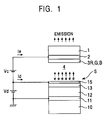
- an electron emission device having the MIS structure has a diode structure in which a top electrode 15 that is a metal thin-film electrode on the top is at a positive potential Vd and in which a bottom electrode 11 that is an ohmic electrode on a backside substrate 10 of glass is at a ground potential.
- Vd positive potential
- a bottom electrode 11 that is an ohmic electrode on a backside substrate 10 of glass is at a ground potential.
- Electrons "e” emitted by the top electrode 15 of the electron emission device (emission current Ie) are accelerated by a high acceleration voltage Vc applied to a collector electrode (transparent electrode) 2 provided on a front faceplate 1 in a face-to-face relationship with the same and are collected by the collector electrode 2.
- Vc high acceleration voltage
- collector electrode transparent electrode
- visible light associated with the element will be emitted.
- a plurality of electron emission devices having the MIS (or MIM) structure are constructed by sequentially forming a bottom electrode, a semiconductor (or metal) electron supply layer, an insulator layer, and a top electrode on a substrate in each of regions where the top and bottom electrodes intersect each other.
- a front-side substrate 1 has a transparent collector electrode 2 made of an indium tin oxide (so-called ITO), a tin oxide (SnO), a zinc oxide (ZnO) or the like provided therein and receives electrons emitted by electron emission devices S on the backside substrate 10.
- Luminescent materials 3 in R, G and B are applied to the transparent collector electrode 2.
- the pair of the backside and front-side substrates 10 and 1 are held with spacers or the like (not shown) and are sealed with a vacuum space 4 sandwiched therebetween.
- the two types of electrodes i.e., the bottom electrodes 11 and the top electrodes 15 are required on the backside substrate 10 to serve as electrodes for driving the flat panel display device utilizing electron emission devices, and those electrodes are configured to be orthogonal to each other in order to drive the devices in the form of a matrix.
- the top electrodes 15 and bottom electrodes 11 are extended to dispose ends thereof as pickup sections on two sides of the backside substrate 10. The electrodes are connected to the outside at the pickup sections on the two sides.
- an assembled FED has a configuration in which the three types of electrodes, i.e., the bottom electrodes 11, top electrodes 15, and collector electrodes 2 are picked up at the three pickup sections on the three sides.
- electrode pickup sections undesirably overlap each other on three sides when they are assembled into a unit.
- sides of the panels must be tightly combined with each other, and measures must be taken to prevent any overlap between electrode pickup sections, which makes the assembly process very much difficult.
- the present invention has been conceived taking the above situation into consideration, and it is an object of the invention to provide flat panel display devices which can be combined into a unit to serve as a large display device.
- a flat panel display device comprises an emitting region constituted by a plurality of first electrodes provided on a substrate and extending in parallel, a plurality of second electrodes provided on the first electrodes and extending substantially perpendicularly to the first electrodes, and a plurality of emission devices for emitting electrons or light respectively connected to a plurality of intersections between the first and second electrodes and arranged on the substrate and comprising a peripheral region surrounding the emitting region on the substrate, characterized in that the first and second electrodes and a group of second external repeating terminals are collectively arranged side by side in a part of the peripheral region.
- said first external repeating terminals are ends of said first electrodes and wherein said second external repeating terminals are respectively connected to said second electrodes in said emitting region and are provided side by side along said first external repeating terminals.
- said first external repeating terminals and said second external repeating terminals are alternately provided side by side.
- said substrate is a backside substrate; said first electrodes are bottom electrodes; said emission devices are electron emission devices having insulator layers formed on said bottom electrodes and top electrodes; and said second electrodes are connected to said top electrodes, the display device comprising a transparent front-side substrate which faces said top electrodes of said electron emission devices on said backside substrate with a vacuum space sandwiched therebetween.
- said electron emission devices have electron supply layers constituted by a metal or semiconductor provided between said bottom electrodes and said insulator layers.
- said front-side substrate has collector electrodes formed on a surface thereof toward said vacuum space and luminescent layers formed on said collector electrodes.
- said front-side substrate has luminescent layers formed on a surface thereof toward said vacuum space and collector electrodes formed on said luminescent layers.
- the device further comprises insulating protective films provided between said second electrodes and said insulator layers and between said second electrodes and said backside substrate.
- the device further comprises insulating protective films provided between said first electrodes and said second electrodes at intersections between said first electrodes and said second electrodes.
- said emission devices are organic electroluminescence devices having one or more layers of an organic electroluminescence medium sequentially formed between said first and second electrodes.
- said substrate and said first electrodes are transparent.
- said first electrodes comprise a plurality of transparent electrodes associated with each of said organic electroluminescence devices and a metal bus line for electrically connecting said transparent electrodes.
- said second electrodes are transparent.
- said emitting region is in a rectangular configuration and wherein the first and second external repeating terminals collectively provided side by side in a part of said peripheral region are located on one side of said rectangle.
- said first and second external repeating terminals have an external terminal exposed to the outside.
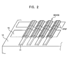
- a flat panel display device utilizing electron emission devices or sites has a pair of a backside substrate 10 and a transparent front-side substrate 1 which face each other with a vacuum space sandwiched therebetween.
- the front-side substrate having collector electrodes 2 provided on an inner surface thereof is provided such that it faces top electrodes 15 of electron emission sites on the backside substrate 10 with the vacuum space sandwiched therebetween.
- a rectangular emitting region 100 and a peripheral region 101 surrounding the same are provided on an inner surface of the backside substrate 10 of the flat panel display device.
- a predetermined luminescent material (not shown) is applied to the collector electrodes 2 on the front-side substrate 1.
- the emitting region 100 includes a plurality of bottom electrodes (not shown) extending in parallel, a plurality of bus electrodes 16 provided on the bottom electrodes and extending substantially perpendicularly to the same, and a plurality of electron emission sites S respectively connected to regions in the vicinity of intersections between the bottom electrodes and bus electrodes 16. Therefore, the plurality of electron emission sites S are arranged on the backside substrate 10 such that the top electrodes 15 facing the vacuum space form a matrix array.
- An electron emission site S has an insulator layer (not shown) formed on the bottom electrode and a top electrode 15, and a bus electrode 16 is connected to the top electrode 15.
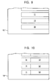
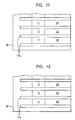
- a plurality of first external repeating terminals 18 that are extensions of the bottom electrodes are collectively arranged side by side on one side of the peripheral region 101 of the backside substrate 10.
- a plurality of second external repeating terminals 19 are respectively connected to the bus electrodes 16 in the emitting region 100 and are arranged side by side along the first external repeating terminals 18.
- the first and second external repeating terminals 18 and 19 extend in the same direction from one side of the emitting region 100.
- the first and second external repeating terminals 18 and 19 serve as external terminals such as pickup sections or wiring pads when they are exposed.
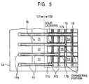
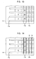
- a second external repeating terminal 19 branches from the bus electrode 16 on each line connected to the top electrode 15 to form of the letter "T" between bottom electrodes 11, and it is picked up from the panel at a pickup section of a bottom electrode 11 or a region close to a first external repeating terminal 18.
- the flat panel display device has a configuration in which second insulating protective films 17b are provided under the bus electrodes 16 and first insulating protective films 17a are also provided under the second external repeating terminals 19 to prevent them from shorting with the bottom electrodes 11.
- a third insulating protective film 17c is provided separately from the first and second insulating protective films 17a and 17b under a second external repeating terminal 19 which intersects with any bus electrode 16 that should not be connected in order to prevent it from shorting with the bus electrode 16.
- the intersection between the bus electrode 16 and the second external repeating terminal 19 which should not be connected becomes a solid crossing.
- Fig. 6 shows a connecting a region or a connecting section where a second external repeating terminal 19 branches from a bus electrode 16 in the form of the letter "T".
- Fig. 7 shows a solid crossing between a second external repeating terminal 19 and a bus electrode 16.
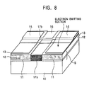
- Fig. 8 shows a connecting section between a second external repeating terminal 19 and a bus electrode 16 and an intersection between a bottom electrode 11 and the bus electrode 16.
- a first insulating protective film 17a under the second external repeating terminal 19 is formed such that it extends to cover at least a precipice portion in a part of the bottom electrode 11. Therefore, each electron emission site S formed by an electron supply layer 12.
- an insulator layer 13, and a top electrode 15 sequentially formed on a bottom electrode 11 is independently formed on a surface of the backside substrate 10 on the side of the vacuum space.
- the bus electrodes 16 are formed such that each of them extends on the second insulating protective films 17b to independently establish electrical connection between adjoining top electrodes 15.
- the bus electrodes 16 are provided over the first insulating protective films 17a and second insulating protective films 17b such that they are not in contact with the backside substrate 10.
- the top electrodes 15 formed on the insulator layer 13 are formed only in flat regions of the insulator layer at spaces associated with sub-pixels.
- the top electrodes 15 are formed on the flat surfaces of the insulator layer 13 with a uniform thickness without shaping the top electrodes themselves in the form of stripes. This makes it possible to generate a uniform electric field when they are driven.
- the connecting section (precipice portion) of each top electrode 15 is formed on the bus electrode 16 which is sufficiently thick.
- the bus electrode 16 connects the top electrodes 15 of adjoining devices.
- the bus electrode 16 is formed to cross a precipice portion that is formed because of the thickness of a bottom electrode, a semiconductor electron supply layer, and an insulator layer, since a sufficiently thick first insulating protective film 17a is provided under the bus electrode 16, any shorting between the electrode and the bottom electrode 11 or semiconductor electron supply layer 12 is prevented.
- the thickness of the bus electrodes 16 relative to the panel size may be any value as long as no problem associated with resistance occurs, a preferable thickness ranging from 0.1 to 50 ⁇ m.
- the first insulating protective film 17a under the bus electrodes 16 may be provided before or after the insulator layer 13 at the pixel region is formed.
- the insulating protective films 17a make it possible to provide a device structure in which the bus electrodes 16 are not damaged because of the presence of the precipice.
- layers of Cr, Cu and Cr are used as materials for the bus electrodes, it is not limited to use such materials, and any metal such as Pt, Au, W, Ru, Ir, Al, Sc, Ti, V, Mn, Fe, Co, Ni, Zn, Ga, Y, Zr, Nb, Mo, Tc, Rh, Pd, Ag, Cd. Ln, Sn, Ta, Re, Os, Tl, Pb, La, Ce, Pr, Nd, Pm, Sm, Eu, Gd, Tb, Dy, Ho, Er, Tm, Yb or Lu may be used alone. Alternatively, or any compound or layers of such metals may be used.
- any metal such as Pt, Au, W, Ru, Ir, Al, Sc, Ti, V, Mn, Fe, Co, Ni, Zn, Ga, Y, Zr, Nb, Mo, Tc, Rh, Pd, Ag, Cd. Ln, Sn, Ta, Re, Os, Tl, Pb, La, Ce, Pr
- bus electrodes such that they contact one end of the top electrodes 15 (pixel region) as illustrated, and they may be formed to surround the top electrodes 15.
- the second insulating protective films under the bus electrodes 16 may be also formed to surround the top electrodes 15.
- Silicon oxide SiO x (wherein subscribed x represents an atomic ratio) is effective as the dielectric material of the first, second, and third insulating protective films 17a, 17b, and 17c and, metal oxides or metal nitrides such as LiO x , LiN x , NaO x , KO x , RbO x , CsO x , BeO x , MgO x , MgN x , CaO x , CaN x , SrO x , BaO x , ScO x , YO x , YN x , LaO x , LaN x , CeO x , PrO x , NdO x , SmO x , EuO x , GdO x , TbO x , DyO x , HoO x , ErO x , TmO x , YbO x
- metal complex oxides such LiAlO 2 , Li 2 SiO 3 , Li 2 TiO 3 , Na 2 Al 22 O 34 , NaFeO 2 , Na 4 SiO 4 , K 2 SiO 3 , K 2 TiO 3 , K 2 WO 4 , Rb 2 CrO 4 , Cs 2 CrO 4 , MgAl 2 O 4 , MgFe 2 O 4 , MgTiO 3 , CaTiO 3 , CaWO 4 , CaZrO 3 , SrFe 12 O 19 , SrTiO 3 , SrZrO 3 , BaAl 2 O 4 , BaFe 12 O 19 , BaTiO 3 , Y 3 Al 5 O 12 , Y 3 Fe 5 O 12 , LaFeO 3 , La 3 Fe 5 O 12 , La 2 Ti 2 O 7 , CeSnO 4 , CeTiO 4 , Sm 3 Fe 5 O 12 , EuFeO 3 , Eu 3 Fe 5
- fluorides such as LiF, MgF 2 , SmF 3 and the like, chlorides such as HgCl. FeCl 2 , CrCl 3 and the like, bromides such as AgBr, CuBr, MnBr 2 and the like, iodide such as PbI 2 , CuI, FeI 2 and the like and metal oxidized nitrides such as SiAlON and the like can be used as well for dielectric material of the insulator layer 13.
- Ceramics such as Al 2 O 3 , Si 3 N 4 and BN an the like may be used for the material of the backside substrate 10 instead of glass.
- the layers of Cr, Cu and Cr are used as materials for the bottom electrode 11, it is not limited to use such materials, and any metal such as Pt, Au, W, Ru, Ir, Al, Sc, Ti, V, Mn, Fe, Co, Ni, Zn, Ga, Y, Zr, Nb, Mo, Tc, Rh, Pd, Ag, Cd, Ln, Sn. Ta, Re, Os, Tl, Pb, La, Ce, Pr, Nd, Pm, Sm, Eu, Gd, Tb, Dy, Ho, Er, Tm, Yb or Lu may be used alone.
- Metals Pt, Au, W, Ru and Ir are effective as the material for the top electrode 15 on the electron emission side.
- Al, Sc, Ti, V, Cr, Mn, Fe, Co, Ni, Cu, Zn, Ga, Y, Zr, Nb, Mo, Tc, Rh, Pd, Ag, Cd, Ln, Sn, Ta, Re, Os, Tl, Pb, La, Ce, Pr, Nd, Pm, Sm, Eu, Gd, Tb, Dy, Ho, Er, Tm, Yb, Lu and the like can be used as well for the thin-film top electrode 15.
- Amorphous silicon is an advantageous material for the electron supply layers 12 of the electron emission sites.
- the hydrogenated amorphous silicon (so-called a-Si:H) in which almost of the dangling bonds of a-Si are terminated by hydrogen atoms is effective for the electron supply layers 12.
- hydrogenated amorphous silicon carbide (so-called a-SiC:H) in which parts of Si atoms are replaced by carbon atoms (C) is also effectively used for the electron-supply layer 12.
- a-SiN:H hydrogenated amorphous silicon nitride in which parts of Si atoms are replaced by nitrogen atoms (N) may be also effectively used for the electron-supply layer 12.
- silicon doped with boron and/or antimony may be used for the electron-supply layer 12.
- SiO x is used as a dielectric material for the insulator layer 13.
- materials such as metal oxides or metal nitrides, metal complex oxides, sulfides, halides, or metal oxidized nitrides used for the dielectric material of the first, second and third insulating protective films 17a, 17b, and 17c are effective for the insulator layer 13.
- carbon such as diamond, Fullerene (C 2n ), carbon nano-tube and the like or metal carbide such as Al 4 C 3 , B 4 C, CaC 2 , Cr 3 C 2 , Mo 2 C, MoC, NbC, SiC, TaC, TiC, VC, W 2 C, WC, ZrC and the like are also effective as the dielectric material of the insulator layer 13.
- Fullerene (C 2n ) consists of carbon atoms.
- the representative C 60 is a spherical surface basket molecule as known a soccer ball molecule. There is also known C 32 to C 960 and the like.
- the subscribed x in O x , N x and the like in the above chemical formulas represent atomic ratios and also herein after.
- the film thickness of the insulator layer 13 may be 50 nm or greater preferably in ranging from 100 to 1000 nm.
- sputtering is particularly effective in the fabrication of those layers and the substrate, vacuum deposition, CVD (Chemical Vapor Deposition), laser ablation, MBE (Molecular Beam Epitaxy) and ion beam sputtering are also effective.
- a plurality of bottom electrodes 11 in the form of stripes are formed in parallel on a glass substrate 10 which has been cleaned.
- they may be formed only in bottom electrode forming regions using a mask, for example.
- a method may be employed in which an electrode film is formed on the entire surface of a substrate and in which the film is then etched in various ways using a mask to leave only bottom electrode regions.
- an electron supply layer 12 is formed through etching on each of the bottom electrode surface 11 thus fabricated such that it extends along the bottom electrode 11 except a region of the same which is to serve as pickup section or a first external repeating terminal 18 later.
- first insulating protective films 17a are formed on precipice portions defined between the electron supply layers 12 in the form of stripes as a result of the formation of the bottom electrodes 11 and electron supply layers 12 and on the substrate 10 at the bottom of the same.
- the entire surface of the substrate 10 is covered by the first insulating protective films 17a.
- the thickness of the first insulating protective films 17a may be set at a value that is similar to or greater than the thickness up to the electron supply layer 12.
- the bus electrodes 16 which are arranged in parallel in the direction orthogonal to the direction of the bottom electrodes 11 must be formed at a later step.
- the breakage of the bus electrodes 16 located on the top of the panel attributable to the difference between the thicknesses of the bottom electrodes 11 and electron supply layers 12 is prevented by providing the first insulating protective films 17a.
- etching is performed to form the insulator layer 13 on each of the electron supply layer 12 such that it is defined along the electron supply layer.
- the second insulating protective films 17b for the bus electrodes to be formed at a later step are formed on the first insulating protective films 17a and the insulator layer 13 such that they extend in the direction orthogonal to the bottom electrodes.
- the insulator layer 13 is exposed between the second insulating protective films 17b to define electron emitting sections.
- the bus electrodes 16 having a predetermined thickness are formed only on the second insulating protective films 17b such that they are defined along the same. That is, the width of the bus electrodes 16 is smaller than the width of the second insulating protective films 17b.
- the third insulating protective films 17c are formed at intersections of the bus electrodes 16 which should not to be connected to the second external repeating terminals 19 to be connected at a later step.
- the second external repeating terminals 19 having a predetermined thickness are formed only on the first insulating protective films 17a and the third insulating protective films 17c on the bus electrodes 16 which should not be connected such that they are defined along those films. That is, the width of the second external repeating terminals 19 is smaller than the width of the first insulating protective films 17a and the third insulating protective films 17c. Ends of predetermined second external repeating terminals 19 are connected only to predetermined bus electrodes 16.
- the top electrodes 15 are formed as individual electrodes in the form of islands to be linked by the bus electrodes 16.
- Each of the top electrodes 15 is formed across the bus electrodes 16, second insulating protective films 17b, and insulator layer 13 such that a major part of the same is located on a flat surface of the insulator layer 13 and such that an edge of the same covers a part of a bus electrode 16. Since such a panel structure allows the first and second electrodes to be picked up at one side of the panel, electrodes including acceleration electrodes can be taken out only on two sides of panels, which makes it easy to assemble the panels into a unit.
- the first insulating protective films 17a isolate the bus electrodes 16 and isolate adjoining devices from each other, and the second insulating protective films 17b isolate the bus electrodes 16 from the insulator layer 13. Since the distance from the electron supply layer 12 to the top electrode 15 in a region where the second insulating protective film 17b is formed is greater than a similar distance in a region where no second insulating protective film 17b is formed, it is possible to prevent a leak current from the bottom of the bus electrodes 16 and the bottom of the top electrodes 15 on the way to the emitting section.
- the front-side substrate is fabricated by forming the transparent collector electrodes 2 on the transparent front-side substrate 1 made of glass or the like. While any material exhibiting high transmittance against visible light and a low electrical resistance may be used as the transparent collector electrodes 2, in particular, ITO is the optimum material.
- the transparent collector electrodes 2 are formed on the entire surface of the front-side substrate to a thickness of 0.4 ⁇ m.
- the backside substrate and front-side substrate thus fabricated are combined such that a partition wall (not shown) on the backside substrate 10 and a second partition wall (not shown) on the front-side substrate 1 are in contact with each other and such that the two substrates face each other with the vacuum space 4 sandwiched therebetween; the substrates are sealed at the periphery thereof; evacuation is carried out between the two substrates; and a getter provided therein is thereafter scattered through induction heating; and the exhaust port is finally sealed.
- the bottom electrodes and bus electrodes.on the backside substrate are respectively connected to the ground and a positive voltage, and the transparent electrodes on the front-side substrate are connected to a positive voltage of a few kV, to complete a flat panel display device consisting of a pair of a transparent front-side substrate 1 and a backside substrate 10 as shown in Fig. 4.
- the thickness of the first insulating protective films 17a in the above-described embodiment may be set at a value that is similar to or greater than the thickness up to the electron supply layer 12 as shown in Fig. 6, this is not limiting the present invention.
- breakage of the bus electrodes can be avoided if the films have a thickness that is 5 % or more of the thickness of the electron emission sites as'shown in Fig. 17. Therefore, the thickness of the first insulating protective films is preferably 5 % or more of the thickness of the devices as a whole (about 6 ⁇ m) (the upper liming being a thickness that is substantially equal to the height of the device insulator layer 13).
- the lower limit for the thickness of the first insulating protective films 17a is a thickness which does not cause breakage of the bus electrodes.
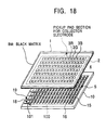
- luminescent material layers 3R, 3G, and 3B respectively emitting red, green, and blue light may be provided in regions defined by a black matrix BM made of carbon or the like on an inner surface of a front-side substrate 1, and conductor layers made of Al or the like may be provided on the inner surface to be used as collector electrodes 2 as shown in Fig. 18.
- an image display array constituted by a plurality of light-emitting sections associated with the luminescent material layers 3R, 3G, and 3B is defined by the matrix layer BM in a dark color or black, they may be similarly defined using a stripe layer in a dark color or black. In either case, there is provided a flat panel display device utilizing electron emission sites having an image display array constituted by a plurality of light-emitting sections associated with the luminescent material layers.
- a flat panel display device was actually fabricated with specifications (1) through (6) as shown below using a sputtering process for film formation and then characteristics of the same were examined.
- the bottom electrodes (1) and semiconductor electron supply layers (2) were formed in the form of lines on a glass substrate which had been cleaned. Thereafter, the first insulating protective films (7) were formed between the lines. Next, the insulator layers (3) were formed on the semiconductor electron supply layers (2) in the form of lines such that they are defined along the same. Next, the second insulating protective films (7) were formed on the first insulating protective films (7) and the insulator layers (3) in the form of line orthogonal thereto. Those protective films formed a grid configuration constituted by regions orthogonal to the bottom electrodes (1) and regions extending between the bottom electrodes (1) in parallel therewith, and the parallel regions covered precipice portions formed between the bottom electrodes (1) and the semiconductor layers (2).
- bus electrodes (5) were formed on the second insulating protective films (7) orthogonal to the bottom electrodes (1) such that they were defined along the same.
- the second external repeating terminals (6) were formed on the first insulating protective films (7) between the bottom electrodes (1) and on the predetermined regions on the bus electrodes (5) such that they are connected to each of the bus electrodes in an orthogonal relationship.
- the top electrode (4) was formed for each of the light-emitting sections such that it covers a flat region of the semiconductor electron supply layer (2) and a part of the bus electrode (5).
- the glass (backside) substrate formed with an emission site comprised of a plurality of electron emission sites and a separately fabricated front-side substrate applied with luminescent materials serving as pixels capable of emitting R, G, and B light were disposed such that they sandwich spacers made of glass. They are heated and bonded together in a high level of vacuum of 1 X 10 -7 torr to form a panel. A high level of vacuum was maintained inside the panel using a non-evaporating getter.
- a voltage of 5 kV as an acceleration voltage was applied to the flat panel display device thus fabricated, and electrical characteristics, i.e., a driving voltage, a device current, and an emission current were examined.
- the display device had characteristics equivalent to those of the characteristics of conventional devices as shown in Fig. 19.
- the number of the second external repeating terminals 19 formed between a pair of bottom electrodes 11 may be increased according to the number of the top electrodes.
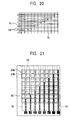
- Fig. 20 that is a schematic view showing only the bottom electrodes 11, bus electrodes 16, and the second external'repeating terminals 19, two second external repeating terminals 19 may be provided between each pair of adjoining bus electrodes 16.
- the scope of the invention includes a flat panel display device constituted by a plurality of organic EL devices having at least one layer of an organic EL medium and second electrodes formed in the same order on first electrodes instead of electron emission sites.
- Fig. 21 is a partially cutaway schematic enlarged plan view of a part of a flat panel display device constituted by a plurality of organic EL devices according to the invention as viewed from a substrate thereof. As apparent from the partial enlarged sectional view shown in Fig. 22, such a flat panel display device is manufactured as follows.
- a transparent substrate 20 made of glass or the like is provided, and a plurality of island-shaped transparent electrodes 23a made of a material having a high work function such as ITO are formed on a principal surface thereof in the form of a matrix to serve as an image display array region.
- metal anode bus lines 23b for electrically connecting the island-shaped transparent electrodes 23a in the horizontal direction are formed through vacuum deposition or the like.
- steps similar to those shown in Figs. 14 and 15 for explaining the above embodiments are performed to branch a second external repeating terminal 19 from each of the anode bus lines such that it extends perpendicularly to the anode bus line 23b and such that it is located between a pair of island-shaped transparent electrodes.
- a plurality of partition walls 27 having electrical insulating properties are formed on the'second external repeating terminals 19 to cover the same.
- a deposition process utilizing a predetermined mask is performed to form an organic EL medium 28 having a predetermined thickness on ITO electrodes 23 exposed between the partition walls 27.
- Cathodes of a plurality of second display electrodes 29 are formed through deposition or the like on the thin films of the organic EL medium such that they expend perpendicularly thereto to define a light-emitting section at each of intersections of the same with the first display electrodes.
- Sections of the organic EL medium 28 thus surrounded by the first and second display electrodes intersecting each other correspond to the light-emitting sections.
- the substrate and the first display electrodes are transparent, and light is emitted from the substrate.
- the second display electrodes may conversely be formed from a transparent material to emit light from the second display electrodes.
- a conductor film is formed on the second electrode films, and an anti-humidity process and sealing is thereafter performed to complete the organic EL display panel.
- the present invention may be applied to a plasma display device which is a flat panel display device comprising an emitting region constituted by a plurality of first electrodes provided on a substrate and extending in parallel, a plurality of second electrodes provided on the first electrodes and extending substantially perpendicularly to the first electrodes, and a plurality of emission sites for emitting ultraviolet light respectively connected to a plurality of intersections between the first and second electrodes and arranged on the substrate and comprising a peripheral region surrounding the emitting region on the substrate, the display device having a plurality of first external repeating terminals which are formed by extending either of the first and second electrodes and collectively arranging them side by side in a part of the peripheral region and a plurality of second external repeating terminals which are respectively connected to the remaining group of electrodes, i.e., the first or second electrodes in the emitting region and arranged side by side along the first external repeating terminals.
- the invention is different from the conventional methods for picking up electrodes from FEDs in which electrode pickup sections are undesirably overlap each other when the FEDs are assembled into a unit in that the panel structure according to the invention makes it possible to assemble a unit easily because electrodes can be picked up on two sides of panels.
Landscapes
- Engineering & Computer Science (AREA)
- Chemical & Material Sciences (AREA)
- Nanotechnology (AREA)
- Physics & Mathematics (AREA)
- Crystallography & Structural Chemistry (AREA)
- Theoretical Computer Science (AREA)
- Mathematical Physics (AREA)
- Plasma & Fusion (AREA)
- Cathode-Ray Tubes And Fluorescent Screens For Display (AREA)
- Electrodes For Cathode-Ray Tubes (AREA)
- Electroluminescent Light Sources (AREA)
- Devices For Indicating Variable Information By Combining Individual Elements (AREA)
- Cold Cathode And The Manufacture (AREA)
Abstract
Description
Claims (15)
- A display device comprising:an emitting region constituted by
a plurality of first electrodes provided on a substrate and extending in parallel,
a plurality of second electrodes provided on said first electrodes and extending substantially perpendicularly to said first electrodes, and a plurality of emission sites for emitting electrons or light respectively connected to a plurality of intersections between said first and second electrodes and arranged on said substrate; anda peripheral region surrounding said emitting region on said substrate, wherein first and second groups of external repeating terminals for said first and second electrodes are collectively provided side by side in a part of said peripheral region. - A display device according to claim 1, wherein said first external repeating terminals are ends of said first electrodes and wherein said second external repeating terminals are respectively connected to said second electrodes in said emitting region and are provided side by side along said first external repeating terminals.
- A display device according to claim 1, wherein said first external repeating terminals and said second external repeating terminals are alternately provided side by side.
- A display device according to claim 1, wherein said substrate is a backside substrate; said first electrodes are bottom electrodes; said emission sites are electron emission sites having insulator layers formed on said bottom electrodes and top electrodes; and said second electrodes are connected to said top electrodes, the display device comprising a transparent front-side substrate which faces said top electrodes of said electron emission sites on said backside substrate with a vacuum space sandwiched therebetween.
- A display device according to claim 4, wherein said electron emission sites have electron supply layers constituted by a metal or semiconductor provided between said bottom electrodes and said insulator layers.
- A display device according to claim 4, wherein said front-side substrate has collector electrodes formed on a surface thereof toward said vacuum space and luminescent layers formed on said collector electrodes.
- A display device according to claim 4, wherein said front-side substrate has luminescent layers formed on a surface thereof toward said vacuum space and collector electrodes formed on said luminescent layers.
- A display device according to claim 4, further comprising insulating protective films provided between said second electrodes and said insulator layers and between said second electrodes and said backside substrate.
- A display device according to claim 4, further comprising insulating protective films provided between said first electrodes and said second electrodes at intersections between said first electrodes and said second electrodes.
- A display device according to claim 1, wherein said emission sites are organic electroluminescence devices having one or more layers of an organic electroluminescence medium sequentially formed between said first and second electrodes.
- A display device according to claim 10, wherein said substrate and said first electrodes are transparent.
- A display device according to claim 10, wherein said first electrodes comprise a plurality of transparent electrodes associated with each of said organic electroluminescence devices and a metal bus line for electrically connecting said transparent electrodes.
- A display device according to claim 10, wherein said second electrodes are transparent.
- A display device according to claim 1,
wherein said emitting region is in a rectangular configuration and wherein the first and second external repeating terminals collectively provided side by side in a part of said peripheral region are located on one side of said rectangle. - A display device according to any of Claims 1 through 3, wherein said first and second external repeating terminals have an external terminal exposed to the outside.
Applications Claiming Priority (2)
| Application Number | Priority Date | Filing Date | Title |
|---|---|---|---|
| JP2000401724 | 2000-12-28 | ||
| JP2000401724A JP2002202732A (en) | 2000-12-28 | 2000-12-28 | Flat panel display |
Publications (2)
| Publication Number | Publication Date |
|---|---|
| EP1220278A2 true EP1220278A2 (en) | 2002-07-03 |
| EP1220278A3 EP1220278A3 (en) | 2006-03-08 |
Family
ID=18866116
Family Applications (1)
| Application Number | Title | Priority Date | Filing Date |
|---|---|---|---|
| EP01130624A Withdrawn EP1220278A3 (en) | 2000-12-28 | 2001-12-27 | Flat panel display device |
Country Status (3)
| Country | Link |
|---|---|
| US (1) | US6787992B2 (en) |
| EP (1) | EP1220278A3 (en) |
| JP (1) | JP2002202732A (en) |
Cited By (1)
| Publication number | Priority date | Publication date | Assignee | Title |
|---|---|---|---|---|
| EP1677358A3 (en) * | 2004-12-28 | 2011-01-05 | LG Electronics, Inc. | Organic electroluminescence device and method of manufacturing the same |
Families Citing this family (26)
| Publication number | Priority date | Publication date | Assignee | Title |
|---|---|---|---|---|
| US6610354B2 (en) * | 2001-06-18 | 2003-08-26 | Applied Materials, Inc. | Plasma display panel with a low k dielectric layer |
| US7476925B2 (en) | 2001-08-30 | 2009-01-13 | Micron Technology, Inc. | Atomic layer deposition of metal oxide and/or low asymmetrical tunnel barrier interploy insulators |
| TW546853B (en) * | 2002-05-01 | 2003-08-11 | Au Optronics Corp | Active type OLED and the fabrication method thereof |
| US7589029B2 (en) | 2002-05-02 | 2009-09-15 | Micron Technology, Inc. | Atomic layer deposition and conversion |
| US7160577B2 (en) | 2002-05-02 | 2007-01-09 | Micron Technology, Inc. | Methods for atomic-layer deposition of aluminum oxides in integrated circuits |
| CN100401518C (en) * | 2002-09-20 | 2008-07-09 | 皇家飞利浦电子股份有限公司 | Electronic device and method of manufacturing electronic device |
| JP4179138B2 (en) * | 2003-02-20 | 2008-11-12 | 松下電器産業株式会社 | Plasma display panel |
| US7192892B2 (en) | 2003-03-04 | 2007-03-20 | Micron Technology, Inc. | Atomic layer deposited dielectric layers |
| JP4624653B2 (en) * | 2003-05-20 | 2011-02-02 | 出光興産株式会社 | Organic electroluminescence element and display device |
| JP2005100916A (en) * | 2003-08-29 | 2005-04-14 | Toyota Industries Corp | Organic electroluminescence device |
| JP4131218B2 (en) * | 2003-09-17 | 2008-08-13 | セイコーエプソン株式会社 | Display panel and display device |
| KR100536198B1 (en) * | 2003-10-09 | 2005-12-12 | 삼성에스디아이 주식회사 | Plasma display panel |
| JP2005285971A (en) * | 2004-03-29 | 2005-10-13 | Nec Electronics Corp | Semiconductor device |
| TWI244106B (en) * | 2004-05-11 | 2005-11-21 | Ind Tech Res Inst | Triode CNT-FED structure gate runner and cathode manufactured method |
| TWI227094B (en) * | 2004-06-03 | 2005-01-21 | Au Optronics Corp | Organic light-emitting display device and fabricating thereof |
| JP2006107741A (en) * | 2004-09-30 | 2006-04-20 | Hitachi Ltd | Image display device and manufacturing method thereof |
| JP2006107746A (en) * | 2004-09-30 | 2006-04-20 | Hitachi Ltd | Image display device |
| US7803254B2 (en) * | 2004-12-30 | 2010-09-28 | E. I. Du Pont De Nemours And Company | Processes for forming electronic devices and electronic devices formed by such processes |
| TWI253878B (en) * | 2005-03-09 | 2006-04-21 | Au Optronics Corp | Organic electroluminescent element and display device including the same |
| US7687409B2 (en) | 2005-03-29 | 2010-03-30 | Micron Technology, Inc. | Atomic layer deposited titanium silicon oxide films |
| US7662729B2 (en) | 2005-04-28 | 2010-02-16 | Micron Technology, Inc. | Atomic layer deposition of a ruthenium layer to a lanthanide oxide dielectric layer |
| US7572695B2 (en) | 2005-05-27 | 2009-08-11 | Micron Technology, Inc. | Hafnium titanium oxide films |
| US7927948B2 (en) | 2005-07-20 | 2011-04-19 | Micron Technology, Inc. | Devices with nanocrystals and methods of formation |
| US20070023765A1 (en) * | 2005-07-29 | 2007-02-01 | Thomas Alan C | Acicular ITO for LED array |
| US7544596B2 (en) | 2005-08-30 | 2009-06-09 | Micron Technology, Inc. | Atomic layer deposition of GdScO3 films as gate dielectrics |
| TWI677669B (en) * | 2016-09-20 | 2019-11-21 | 友達光電股份有限公司 | Pressure sensing array and pressure sensing method |
Family Cites Families (8)
| Publication number | Priority date | Publication date | Assignee | Title |
|---|---|---|---|---|
| US2967248A (en) * | 1956-09-06 | 1961-01-03 | Rca Corp | Electroluminescent device |
| JP2852357B2 (en) * | 1995-03-09 | 1999-02-03 | 双葉電子工業株式会社 | Display device |
| US5628662A (en) * | 1995-08-30 | 1997-05-13 | Texas Instruments Incorporated | Method of fabricating a color field emission flat panel display tetrode |
| US6118417A (en) * | 1995-11-07 | 2000-09-12 | Micron Technology, Inc. | Field emission display with binary address line supplying emission current |
| JPH1063198A (en) * | 1996-08-19 | 1998-03-06 | Denso Corp | Matrix EL display device |
| JPH10240162A (en) * | 1997-02-28 | 1998-09-11 | Sony Corp | Active matrix display device |
| JPH1167064A (en) * | 1997-08-08 | 1999-03-09 | Pioneer Electron Corp | Electron emitting element and display device using the same |
| JP3483526B2 (en) * | 1999-10-21 | 2004-01-06 | シャープ株式会社 | Image forming device |
-
2000
- 2000-12-28 JP JP2000401724A patent/JP2002202732A/en active Pending
-
2001
- 2001-12-27 EP EP01130624A patent/EP1220278A3/en not_active Withdrawn
- 2001-12-28 US US10/028,994 patent/US6787992B2/en not_active Expired - Fee Related
Cited By (1)
| Publication number | Priority date | Publication date | Assignee | Title |
|---|---|---|---|---|
| EP1677358A3 (en) * | 2004-12-28 | 2011-01-05 | LG Electronics, Inc. | Organic electroluminescence device and method of manufacturing the same |
Also Published As
| Publication number | Publication date |
|---|---|
| US6787992B2 (en) | 2004-09-07 |
| EP1220278A3 (en) | 2006-03-08 |
| JP2002202732A (en) | 2002-07-19 |
| US20020117963A1 (en) | 2002-08-29 |
Similar Documents
| Publication | Publication Date | Title |
|---|---|---|
| US6787992B2 (en) | Display device of flat panel structure with emission devices of matrix array | |
| JP3874396B2 (en) | ELECTRON EMITTING ELEMENT, MANUFACTURING METHOD THEREOF, AND DISPLAY DEVICE USING ELECTRON EMITTING ELEMENT | |
| JP3698390B2 (en) | Electron emission display device and electron emission device | |
| US5962959A (en) | Electron emission device and display device for emitting electrons in response to an applied electric field using the electron emission device | |
| JP3765671B2 (en) | Electron emission device and electron emission display device using the same | |
| EP0911854A1 (en) | Electron emission device and display device using the same | |
| US6400070B1 (en) | Electron emission device and display device using the same | |
| US6259198B1 (en) | Flat panel display apparatus with an array of electron emitting devices | |
| US6472803B1 (en) | Electron emission light-emitting device and display apparatus using the same | |
| US6316873B1 (en) | Electron emission device and display device using the same | |
| US6023125A (en) | Electron emission device and display using the same | |
| US6700132B2 (en) | Flat panel display device utilizing electron emission devices | |
| JP4676428B2 (en) | Electron emission device, manufacturing method thereof, and imaging device or display device using electron emission device | |
| JP5026459B2 (en) | ELECTRON EMITTING ELEMENT ARRAY AND METHOD FOR MANUFACTURING THE SAME | |
| JP3488967B2 (en) | Electron emission device flat panel display device | |
| JP3821482B2 (en) | Method for manufacturing electron-emitting device | |
| JPH11185676A (en) | Electron emitting element flat panel display device | |
| JPH11185675A (en) | Electron emitting element flat panel display device | |
| JPH11185678A (en) | Electron emitting element flat panel display device | |
| JP3537634B2 (en) | Method of manufacturing electron-emitting device and method of manufacturing electron-emitting display device | |
| JPH10321125A (en) | Electron emitting element and display device using this |
Legal Events
| Date | Code | Title | Description |
|---|---|---|---|
| PUAI | Public reference made under article 153(3) epc to a published international application that has entered the european phase |
Free format text: ORIGINAL CODE: 0009012 |
|
| AK | Designated contracting states |
Kind code of ref document: A2 Designated state(s): AT BE CH CY DE DK ES FI FR GB GR IE IT LI LU MC NL PT SE TR |
|
| AX | Request for extension of the european patent |
Free format text: AL;LT;LV;MK;RO;SI |
|
| PUAL | Search report despatched |
Free format text: ORIGINAL CODE: 0009013 |
|
| AK | Designated contracting states |
Kind code of ref document: A3 Designated state(s): AT BE CH CY DE DK ES FI FR GB GR IE IT LI LU MC NL PT SE TR |
|
| AX | Request for extension of the european patent |
Extension state: AL LT LV MK RO SI |
|
| RIC1 | Information provided on ipc code assigned before grant |
Ipc: G09G 3/32 20060101ALI20060118BHEP Ipc: H01J 17/49 20060101ALI20060118BHEP Ipc: H01J 1/30 20060101ALI20060118BHEP Ipc: H01J 31/12 20060101AFI20020423BHEP |
|
| 17P | Request for examination filed |
Effective date: 20060519 |
|
| 17Q | First examination report despatched |
Effective date: 20060724 |
|
| AKX | Designation fees paid |
Designated state(s): DE FR GB |
|
| GRAP | Despatch of communication of intention to grant a patent |
Free format text: ORIGINAL CODE: EPIDOSNIGR1 |
|
| STAA | Information on the status of an ep patent application or granted ep patent |
Free format text: STATUS: THE APPLICATION HAS BEEN WITHDRAWN |
|
| 18W | Application withdrawn |
Effective date: 20080610 |