EP1219577A2 - Low temperature sintered ferrite material and ferrite parts using the same - Google Patents
Low temperature sintered ferrite material and ferrite parts using the same Download PDFInfo
- Publication number
- EP1219577A2 EP1219577A2 EP01129759A EP01129759A EP1219577A2 EP 1219577 A2 EP1219577 A2 EP 1219577A2 EP 01129759 A EP01129759 A EP 01129759A EP 01129759 A EP01129759 A EP 01129759A EP 1219577 A2 EP1219577 A2 EP 1219577A2
- Authority
- EP
- European Patent Office
- Prior art keywords
- ferrite
- mol
- ppm
- basis
- range
- Prior art date
- Legal status (The legal status is an assumption and is not a legal conclusion. Google has not performed a legal analysis and makes no representation as to the accuracy of the status listed.)
- Granted
Links
Images
Classifications
-
- C—CHEMISTRY; METALLURGY
- C04—CEMENTS; CONCRETE; ARTIFICIAL STONE; CERAMICS; REFRACTORIES
- C04B—LIME, MAGNESIA; SLAG; CEMENTS; COMPOSITIONS THEREOF, e.g. MORTARS, CONCRETE OR LIKE BUILDING MATERIALS; ARTIFICIAL STONE; CERAMICS; REFRACTORIES; TREATMENT OF NATURAL STONE
- C04B35/00—Shaped ceramic products characterised by their composition; Ceramics compositions; Processing powders of inorganic compounds preparatory to the manufacturing of ceramic products
- C04B35/01—Shaped ceramic products characterised by their composition; Ceramics compositions; Processing powders of inorganic compounds preparatory to the manufacturing of ceramic products based on oxide ceramics
- C04B35/26—Shaped ceramic products characterised by their composition; Ceramics compositions; Processing powders of inorganic compounds preparatory to the manufacturing of ceramic products based on oxide ceramics based on ferrites
- C04B35/265—Compositions containing one or more ferrites of the group comprising manganese or zinc and one or more ferrites of the group comprising nickel, copper or cobalt
-
- H—ELECTRICITY
- H01—ELECTRIC ELEMENTS
- H01F—MAGNETS; INDUCTANCES; TRANSFORMERS; SELECTION OF MATERIALS FOR THEIR MAGNETIC PROPERTIES
- H01F1/00—Magnets or magnetic bodies characterised by the magnetic materials therefor; Selection of materials for their magnetic properties
- H01F1/01—Magnets or magnetic bodies characterised by the magnetic materials therefor; Selection of materials for their magnetic properties of inorganic materials
- H01F1/03—Magnets or magnetic bodies characterised by the magnetic materials therefor; Selection of materials for their magnetic properties of inorganic materials characterised by their coercivity
- H01F1/12—Magnets or magnetic bodies characterised by the magnetic materials therefor; Selection of materials for their magnetic properties of inorganic materials characterised by their coercivity of soft-magnetic materials
- H01F1/34—Magnets or magnetic bodies characterised by the magnetic materials therefor; Selection of materials for their magnetic properties of inorganic materials characterised by their coercivity of soft-magnetic materials non-metallic substances, e.g. ferrites
-
- C—CHEMISTRY; METALLURGY
- C04—CEMENTS; CONCRETE; ARTIFICIAL STONE; CERAMICS; REFRACTORIES
- C04B—LIME, MAGNESIA; SLAG; CEMENTS; COMPOSITIONS THEREOF, e.g. MORTARS, CONCRETE OR LIKE BUILDING MATERIALS; ARTIFICIAL STONE; CERAMICS; REFRACTORIES; TREATMENT OF NATURAL STONE
- C04B35/00—Shaped ceramic products characterised by their composition; Ceramics compositions; Processing powders of inorganic compounds preparatory to the manufacturing of ceramic products
- C04B35/01—Shaped ceramic products characterised by their composition; Ceramics compositions; Processing powders of inorganic compounds preparatory to the manufacturing of ceramic products based on oxide ceramics
- C04B35/26—Shaped ceramic products characterised by their composition; Ceramics compositions; Processing powders of inorganic compounds preparatory to the manufacturing of ceramic products based on oxide ceramics based on ferrites
-
- H—ELECTRICITY
- H01—ELECTRIC ELEMENTS
- H01F—MAGNETS; INDUCTANCES; TRANSFORMERS; SELECTION OF MATERIALS FOR THEIR MAGNETIC PROPERTIES
- H01F17/00—Fixed inductances of the signal type
- H01F17/0006—Printed inductances
- H01F17/0013—Printed inductances with stacked layers
-
- H—ELECTRICITY
- H01—ELECTRIC ELEMENTS
- H01F—MAGNETS; INDUCTANCES; TRANSFORMERS; SELECTION OF MATERIALS FOR THEIR MAGNETIC PROPERTIES
- H01F41/00—Apparatus or processes specially adapted for manufacturing or assembling magnets, inductances or transformers; Apparatus or processes specially adapted for manufacturing materials characterised by their magnetic properties
- H01F41/02—Apparatus or processes specially adapted for manufacturing or assembling magnets, inductances or transformers; Apparatus or processes specially adapted for manufacturing materials characterised by their magnetic properties for manufacturing cores, coils, or magnets
- H01F41/04—Apparatus or processes specially adapted for manufacturing or assembling magnets, inductances or transformers; Apparatus or processes specially adapted for manufacturing materials characterised by their magnetic properties for manufacturing cores, coils, or magnets for manufacturing coils
- H01F41/041—Printed circuit coils
- H01F41/046—Printed circuit coils structurally combined with ferromagnetic material
-
- H—ELECTRICITY
- H01—ELECTRIC ELEMENTS
- H01G—CAPACITORS; CAPACITORS, RECTIFIERS, DETECTORS, SWITCHING DEVICES, LIGHT-SENSITIVE OR TEMPERATURE-SENSITIVE DEVICES OF THE ELECTROLYTIC TYPE
- H01G4/00—Fixed capacitors; Processes of their manufacture
- H01G4/40—Structural combinations of fixed capacitors with other electric elements, the structure mainly consisting of a capacitor, e.g. RC combinations
-
- C—CHEMISTRY; METALLURGY
- C04—CEMENTS; CONCRETE; ARTIFICIAL STONE; CERAMICS; REFRACTORIES
- C04B—LIME, MAGNESIA; SLAG; CEMENTS; COMPOSITIONS THEREOF, e.g. MORTARS, CONCRETE OR LIKE BUILDING MATERIALS; ARTIFICIAL STONE; CERAMICS; REFRACTORIES; TREATMENT OF NATURAL STONE
- C04B2235/00—Aspects relating to ceramic starting mixtures or sintered ceramic products
- C04B2235/70—Aspects relating to sintered or melt-casted ceramic products
- C04B2235/72—Products characterised by the absence or the low content of specific components, e.g. alkali metal free alumina ceramics
- C04B2235/724—Halogenide content
-
- C—CHEMISTRY; METALLURGY
- C04—CEMENTS; CONCRETE; ARTIFICIAL STONE; CERAMICS; REFRACTORIES
- C04B—LIME, MAGNESIA; SLAG; CEMENTS; COMPOSITIONS THEREOF, e.g. MORTARS, CONCRETE OR LIKE BUILDING MATERIALS; ARTIFICIAL STONE; CERAMICS; REFRACTORIES; TREATMENT OF NATURAL STONE
- C04B2235/00—Aspects relating to ceramic starting mixtures or sintered ceramic products
- C04B2235/70—Aspects relating to sintered or melt-casted ceramic products
- C04B2235/72—Products characterised by the absence or the low content of specific components, e.g. alkali metal free alumina ceramics
- C04B2235/726—Sulfur content
Definitions
- the present invention relates to a ferrite material for a ceramic inductor, and particularly relates to a ferrite material stable and excellent in temperature characteristic and for use in ferrite sinter used as various magnetic materials, which is capable of being burnt at a low temperature, and ferrite parts such as chip inductors, chip beads parts, composite multi-layer parts, ferrite cores, etc., using the ferrite material.
- multi-layer chip parts such as chip inductors or chip beads parts are usually manufactured as follows. That is, a magnetic substance layer paste and an internal conductor paste are laminated integrally by thick film technology and then burnt, external electrodes are formed by use of an external electrode paste, and the thus integrated lamination is then burnt to thereby manufacture the multi-layer chip part.
- Ni-Cu-Zn ferrite which can be sintered at a temperature low to be not higher than the melting point of Ag composing internal electrodes is generally used as a magnetic material for the magnetic layers.
- Ni-Cu-Zn ferrite or Ni-Zn ferrite When Ni-Cu-Zn ferrite or Ni-Zn ferrite is used, Fe 2 O 3 obtained by thermal decomposition using a hydrochloric acid pickling waste liquor for iron chloride as a starting material, or Fe 2 O 3 obtained by thermal decomposition of iron sulfate obtained from a sulfuric acid pickling waste liquor for steel is used for producing iron oxide which is one of raw materials for the ferrite.
- S or Cl exists in the ferrite raw material inevitably.
- the ferrite affects electromagnetic properties, that is, inductance properties, or sintering properties, that is, density, in accordance with the content of S or Cl (JP-B-2867196 or JP-A-11-144934).
- additives such as glass, bismuth oxide, vanadium oxide, etc.
- sintering auxiliaries such as glass, bismuth oxide, vanadium oxide, etc.
- a ferrite material is generally obtained by mixing an iron compound and other ferrite constituent element compounds, and burning this mixture provisionally.
- this provisionally burning process it is known that the solid phase reaction rate to form spinel crystals varies in accordance with the content of S or Cl contained in the ferrite mixture powder (See JP-A-11-144934). Due to a difference of this reaction rate, a raw material or an intermediate product is residual or out-of-phase is produced by segregation of the raw material or the intermediate product by thermal dissociation. As a result, the powder composition is made uneven to have a bad influence on the sinter density or the magnetic properties.
- the present inventors have found that by regulating the S and Cl contents of ferrite powder in a ferrite material as shown in the following paragraphs (A1) to (A3), it is possible to provide a ferrite material which provides a high density without using any additive, and has a small temperature characteristic in spite of the high density, and it is possible to provide high-performance ferrite parts such as chip inductors, chip beads parts, composite multi-layer parts, ferrite cores, etc., as shown in the following paragraphs (A4) to (A6), by use of this ferrite material.
- a sulfur content of ferrite powder in a raw material stage is in a range of from 300 ppm to 900 ppm on S basis and a chlorine content of the ferrite powder is not higher than 100 ppm on Cl basis, while a sulfur content of a ferrite sinter after burning is not higher than 100 ppm on S basis and a chlorine content of the ferrite sinter is not higher than 25 ppm on Cl basis.
- a sulfur content of ferrite powder in a raw material stage is in a range of from 300 ppm to 900 ppm on S basis and a chlorine content of the ferrite powder is not higher than 100 ppm on Cl basis, while a sulfur content of a ferrite sinter after burning is not higher than 100 ppm on S basis and a chlorine content of the ferrite sinter is lower than 10 ppm on Cl basis.
- the ferrite material has a composition of Fe 2 O 3 ranging from 25 mol% to 52 mol%, ZnO of 40 mol% or lower, CuO of 20 mol% or lower, NiO of 65 mol% or lower, and MgO occupying a remainder.
- a chip part is constituted by a chip inductor or a chip beads part configured by laminating ferrite magnetic layers and internal conductors, wherein the ferrite magnetic layers are composed of a ferrite material defined in any one of the paragraphs (A1) to (A3).
- a composite multi-layer part is constituted by at least an inductor portion configured by laminating ferrite magnetic layers and internal conductors, wherein the ferrite magnetic layers are composed of a ferrite material defined in any one of the paragraphs (A1) to (A3).
- a ferrite core is constituted by a ferrite material defined in any one of the paragraphs (A1) to (A3).
- ferrite materials capable of attaining the object can be provided as shown in the following paragraphs (B1) and (B2), and ferrite parts capable of attaining the object can be provided as shown in the following paragraphs (B3) to (B5).
- (B1) A ferrite material constituted by an Ni ferrite material using a nickel compound as a raw material, the nickel compound having a specific surface area in a range of from 1.0 m 2 /g to 10 m 2 /g and a sulfur content in a range of from 100 ppm to 1,000 ppm on S basis.
- (B2) A ferrite material according to the paragraph (B1), wherein the Ni ferrite material has a composition of Fe 2 O 3 ranging from 25 mol% to 52 mol%, ZnO ranging from 0 mol% to 40 mol%, CuO ranging from 0 mol% to 20 mol%, NiO ranging 1 mol% to 65 mol%, and MgO occupying the remainder.
- (B3) A chip part constituted by a chip inductor or a chip beads part configured by laminating ferrite magnetic layers and internal conductors; wherein the ferrite magnetic layers is composed of: an Ni ferrite material using a nickel compound as a raw material, the nickel compound having a specific surface area in a range of from 1.0 m 2 /g to 10 m 2 /g and a sulfur content in a range of from 100 ppm to 1,000 ppm on S basis; or an Ni ferrite material using a nickel compound as a raw material, the nickel compound having a specific surface area in a range of from 1.0 m 2 /g to 10 m 2 /g and a sulfur content in a range of from 100 ppm to 1, 000 ppm on S basis, the Ni ferrite material having a composition of Fe 2 O 3 ranging from 25 mol% to 52 mol%, ZnO ranging from 0 mol% to 40 mol%, CuO ranging from 0 mol% to 20 mol
- (B4) Acompositemulti-layer part constituted by at least an inductor portion configured by laminating ferrite magnetic layers and internal conductors; wherein the ferrite magnetic layers is composed of: an Ni ferrite material using a nickel compound as a raw material, the nickel compound having a specific surface area in a range of from 1.0 m 2 /g to 10 m 2 /g and a sulfur content in a range of from 100 ppm to 1,000 ppm on S basis; or an Ni ferrite material using a nickel compound as a raw material, the nickel compound having a specific surface area in a range of from 1.0 m 2 /g to 10 m 2 /g and a sulfur content in a range of from 100 ppm to 1,000 ppm on S basis, the Ni ferrite material having a composition of Fe 2 O 3 ranging from 25 mol% to 52 mol%, ZnO ranging from 0 mol% to 40 mol%, CuO ranging from 0 mol% to 20 mol%
- a ferrite core constituted by: an Ni ferrite material using a nickel compound as a raw material, the nickel compound having a specific surface area in a range of from 1.0 m 2 /g to 10 m 2 /g and a sulfur content in a range of from 100 ppm to 1,000 ppm on S basis; or an Ni ferrite material using a nickel compound as a raw material, the nickel compound having a specific surface area in a range of from 1.0 m 2 /g to 10 m 2 /g and a sulfur content in a range of from 100 ppm to 1,000 ppm on S basis, the Ni ferrite material having a composition of Fe 2 O 3 ranging from 25 mol% to 52 mol%, ZnO ranging from 0 mol% to 40 mol%, CuO ranging from 0 mol% to 20 mol%, NiO ranging 1 mol% to 65 mol%, and MgO occupying the remainder.
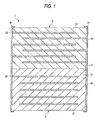
- Fig. 1 is a view showing an example of a composite multi-layer part using a low-temperature sintered and high-performance ferrite material according to the present invention.
- ferrite constituent element compounds for example, Fe 2 O 3 , NiO, CuO, ZnO and MgO are used, weighed to prepare an intended composition after burning, and wet-mixed with pure water by a ball mill or the like.
- the wet-mixed mixture is dried by a spray drier or the like, and then burnt provisionally.
- the provisionally burnt mixture is levigated, and then dried by a spray drier or the like.
- ferrite powder is obtained.
- This ferrite powder which has been pulverized and dried is set to have a sulfur content in a range of from 300 ppm to 900 ppm on S element basis and a chlorine content of 100 ppm or lower on Cl element basis.
- the value of the sinter density is lower than the sinter density 4.85 g/cm 3 guaranteeing the resistance to moisture .
- the sulfur content exceeds 900 ppm, the sinter density becomes high, but the diffusion of Ag or the segregation of Cu increases so that the inductance or the temperature characteristic deteriorates.
- the temperature characteristic indicates a rate of change between inductance measured at 25°C and inductance measured at 85°C with the inductance at 25°C as a reference.
- the temperature characteristic is preferably within ⁇ 3%, more preferably within ⁇ 2%. Accordingly, it is more preferable that the sulfur content is in a range of from 300 ppm to 700 ppm on S basis in the ferrite raw material stage.
- the sulfur content in the ferrite sinter after burning becomes not higher than 100 ppm on S basis, and the chlorine content in the ferrite sinter becomes not higher than 25 ppm on Cl basis.
- the sulfur content in the ferrite sinter exceeds 100 ppm on S basis, the diffusion of Ag into the magnetic substance increases so that the inductance and the temperature characteristic deteriorate.
- the chlorine content exceeds 25 ppm on Cl basis, the sinter density and the temperature characteristic deteriorate.
- the sulfur content may be measured by analyzing SO 2 converted by burning and oxidizing in the oxygen atmosphere by an infrared detector.
- the chlorine content may be measured by extracting Cl by steam distillation and measuring the absorbance of the extracted liquid.
- the spinel synthesis rate means a value expressed by the following expression from peak intensity (Isp311) of a (311) plane of spinel ferrite, peak intensity (IFe104) of a (104) plane of ⁇ -Fe 2 O 3 , and peak intensity (ICu111) of a (111) plane of CuO in powder X ray diffraction.
- the spinel synthesis rate is lower than 96%, plenty of ferrite constituent element compounds are residual so that the sinter density is low. Accordingly, the spinel synthesis rate is preferably not lower than 96%, and more preferably not lower than 99%.
- the ranges of components of the ferrite composition are limited in the present invention for the following reasons. If the principal component Fe 2 O 3 is out of the range of from 25 mol% to 52 mol%, the sinter density becomes low to cause a problem of deterioration of specific permeability, Q, IR (insulation resistance), or the like. If ZnO exceeds 40 mol%, Q is lowered so that the Curie temperature becomes not higher than 100 °C. That is not practical.
- CuO exceeds 20 mol%
- Q is lowered.
- CuO or ZnO is deposited in a bonded surface with a different material such as a capacitor material or the like.
- IR is lowered.
- NiO exceeds 65 mol%
- the ferrite material is not sintered at a temperature not higher than the melting point of Ag.
- MgO is substituted for a part of NiO
- the temperature characteristic is improved while the sinter density and the specific permeability are kept.
- MgO exceeds 15 mol%, the sinter density or the specific permeability deteriorates.
- the content of MgO is preferably not higher than 15 mol%.
- other oxides of Co, Mn, etc. may be contained by about 2 wt% or lower of the whole.
- composition of Fe 2 O 3 , NiO, CuO, ZnO and MgO may be measured by fluorescent X-ray analysis based on a glass beads method.
- ferrite material which provides a high density for ferrite without using any additive, and which has a small temperature characteristic in spite of the high density.
- ferrite cores and multi-layer chip parts composed of this ferrite material are excellent in resistance to moisture and temperature characteristic. Further, the scattering of the sinter density or the inductance can be reduced.
- Respective raw materials were weighed to prepare a composition which would have 49.0 mol% of Fe 2 O 3 , 25.0 mol% of NiO, 12.0 mol% of CuO, and 14.0 mol% of ZnO, after burning.
- MgO was substituted for a part of NiO
- respective raw materials were weighed to prepare a composition which would have 49.0 mol% of Fe 2 O 3 , 20.0 mol% of NiO, 5 mol% of MgO, 12.0 mol% of CuO, and 14.0 mol% of ZnO.
- the respective raw materials were wet-mixed with pure water by a ball mill, and dried by a spray drier. Next, this mixture powder was burnt provisionally at 700 °C to 800 °C for 10 hours. After that, the provisionally burnt powder is levigated with pure water by a ball mill, and dried by a spray drier.
- a multi-layer chip inductor was made up.
- Four parts by weight of ethyl cellulose and 78 parts by weight of terpineol were added to 100 parts by weight of the pulverized powder, and kneaded by a three-roll mill so as to prepare a magnetic substance layer paste.
- 2.5 parts by weight of ethyl cellulose and 40 parts by weight of terpineol were added to 100 parts by weight of Ag having a mean particle size of 0.6 ⁇ m, and kneaded by a three-roll mill so as to prepare an internal electrode paste.
- the magnetic substance layer paste and the internal electrode paste obtained thus were printed alternately so as to be laminated on each other, and burnt at 850 °C for 2 hours.
- a multi-layer chip inductor was obtained.
- This 3216 type (3.2 mm long and 1.6 mm wide) multi-layer chip inductor measured 3.2 mm by 1.6 mm by 1.2 mm, and the number of turns was set to be 9.5.
- external electrodes were formed in end portions of the multi-layer chip inductor by burning at 600 °C.
- Inductance L and Q were measured by means of an LCR meter under the conditions of the measuring frequency 10 MHz and the measuring current 0.1 mA.
- Inductance at 25 °C and inductance at 85 °C were measured in the measuring frequency 1 MHz, and a rate of change with the inductance at 25 °C as a reference was adopted as the temperature characteristic of the inductance of each toroidal shape and each multi-layer chip inductor.
- desired S and Cl contents were obtained by selecting raw materials having different S contents or different Cl contents.
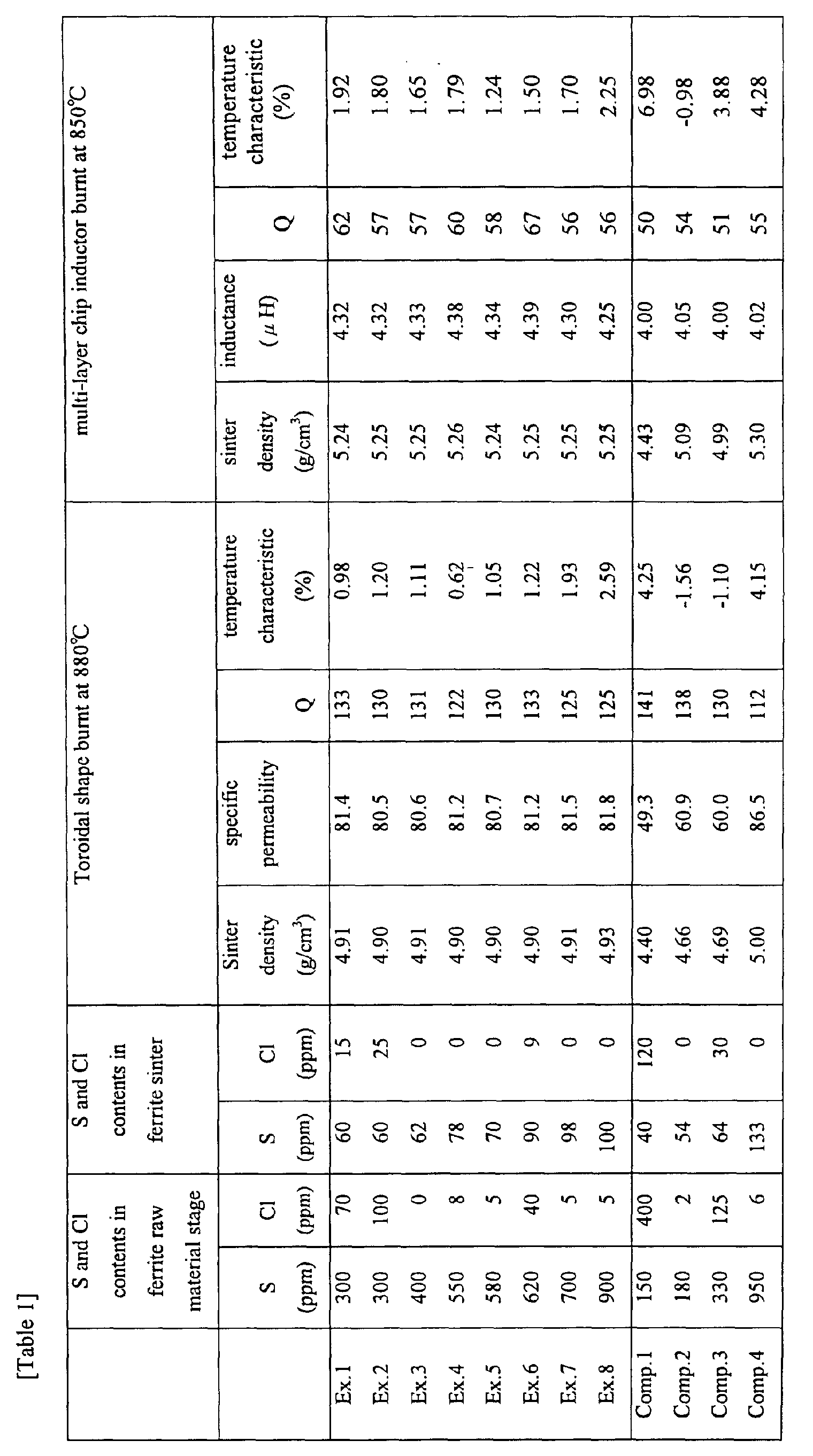
- the sinter density is low to be not higher than 4.85 g/cm 3 in the toroidal shape and not higher than 5.15 g/cm 3 in the multi-layer chip inductor. Thus, the sinter density does not reach a value to be able to guarantee resistance to moisture.
- the temperature characteristic shows a large value, to be not lower than 4%, both in the toroidal shape and in the multi-layer chip inductor.
- the sinter density is low to be not higher than 4.85 g/cm 3 in the toroidal shape and not higher than 5.15 g/cm 3 in the multi-layer chip inductor. Thus, the sinter density does not reach a value to be able to guarantee resistance to moisture.
- the temperature characteristic shows a large value to be not lower than 4% both in the toroidal shape and in the multi-layer chip inductor.
- the sinter density is low to be not higher than 4.85 g/cm 3 in the toroidal shape and not higher than 5.15 g/cm 3 in the multi-layer chip inductor. Thus, the sinter density does not reach a value to be able to guarantee resistance to moisture.
- the sinter density satisfies a value to guarantee the resistance to moisture.
- the electromagnetic property and the temperature characteristic are excellent both in the toroidal shape and in the multi-layer chip inductor.
- the sinter density is not lower than 4.85 g/cm 3 in the toroidal shape and not lower than 5.15 g/cm 3 in the multi-layer chip inductor, while the temperature characteristic is restrained to be within ⁇ 3%.
- An LC composite part 1 shown in Fig. 1 is integrally constituted by a capacitor portion 2 constituted by ceramic dielectric layers 21 and internal electrode layers 25 laminated on each other, and an inductor portion 3 constituted by ceramic magnetic substance layers 31 and internal conductors 35 laminated on each other. External electrodes 51 are formed on the surface of the LC composite part 1.
- the capacitor portion 2 and the inductor portion 3 may have a conventionally known structure. Each of the capacitor portion 2 and the inductor portion 3 is formed into a substantially rectangular shape.
- the dimensions of the LC composite part 1 are not limited particularly, but can be set suitably in accordance with applications. The dimensions of the LC composite part 1 may measure approximately 1.6 ⁇ 10.0 mm by 0.8 ⁇ 15.0 mm by 1.0 ⁇ 5.0 mm.
- the ceramic magnetic substance layers 31 constituting the inductor portion 3 are composed of a ferrite material according to the present invention. That is, a magnetic substance layer paste obtained by kneading the ferrite material according to the present invention with a binder of ethyl cellulose or the like and a solvent of terpineol, butyl carbitol, or the like, is printed and laminated alternately with an internal electrode paste. Thus, the inductor portion 3 is formed.
- the contents of the binder and the solvent in the magnetic substance layer paste are not limited.
- the content of the binder maybe set to be in a range of from 1 wt% to 5 wt%
- the content of the solvent may be set to be approximately in a range of from 10 wt% to 50 wt%.
- the inductor portion 3 may be formed by use of a ceramic magnetic substance layer sheet. That is, slurry obtained by kneading the ferrite material according to the present invention with a binder having polyvinyl butyral or acrylic resin as its principal component and a solvent of toluene, xylene, or the like, in a ball mill, is applied onto a polyester film or the like in a doctor blade method or the like, and dried to obtain a magnetic substance layer sheet.
- the content of the binder in this magnetic substance layer sheet is not limited.
- the content of the binder may be set to be approximately in a range of from 1 wt% to 5 wt%.
- the conductive material composing the internal electrodes 35 of the inductor portion 3 is not limited particularly. It is, however, preferable that the internal electrodes 35 are formed out of a conductive material mainly composed of Ag with a low electric resistivity in order to obtain practical Q for inductor. Ag, Ag alloys, Cu, Cu alloys, etc. are usually used. Each layer of the internal electrodes 35 has an oval shape. Spiral electrical conduction is ensured between adjacent layers of the internal electrodes 35. Thus, the internal electrodes 35 form a closed magnetic path coil (winding pattern). The external electrodes 51 are connected to the opposite ends of the closed magnetic path coil.
- the winding pattern that is, the closed magnetic path shape of the internal conductors 35 can be formed into various patterns.
- the number of turns thereof may be selected suitably in accordance with applications.
- the dimensions, and so on, of respective parts in the inductor portion 3 are not limited, but may be selected suitably in accordance with applications.
- the internal conductors 35 are usually designed so that the thickness is approximately in a range of from 3 ⁇ m to 50 ⁇ m, the winding pitch is approximately in a range of from 10 ⁇ m to 400 ⁇ m, and the number of turns is approximately in a range of from 1.5 to 50.5.
- the magnetic layers 31 are usually designed so that the base thickness is approximately in a range of from 100 ⁇ m to 500 ⁇ m, and the magnetic layer thickness between the internal conductors 35 and 35 is approximately in a range of from 10 ⁇ m to 100 ⁇ m.
- the material used for the ceramic dielectric layers 21 of the capacitor portion 2 is not limited particularly. Although various dielectric materials are available, it is preferable that a titanium oxide dielectric material is used because it has a low burning temperature. Alternatively, titanate composite oxides, zirconate composite oxides, or mixtures thereof may be used. In addition, the material may contain glass such as borosilicate glass in order to reduce the burning temperature.
- TiO 2 or the like containing NiO, CuO, Mn 3 O 4 , Al 2 O 3 , MgO, SiO 2 , or the like, particularly containing CuO, in accordance with necessity, may be used as the titanium oxide dielectric material; BaTiO 3 , SrTiO 3 , CaTiO 3 , MgTiO 3 , or a mixture thereof, may be used as the titanate composite oxide; and BaZrO 3 , SrZrO 3 , CaZrO 3 , MgZrO 3 , or a mixture thereof may be used as the zirconate composite oxide.
- non-magnetic Zn ferrite or the like may be used.
- a dielectric layer paste obtained by kneading the material used for the ceramic dielectric layers 21 of the capacitor portion 2 together with various binders and solvents may be printed and laminated alternately with the internal electrode paste.
- the contents of the binder and the solvent contained in the dielectric layer paste are not limited.
- the content of the binder may be set to be in a range of from 1 wt% to 5 wt%, and the content of the solvent may be set to be approximately in a range of from 10 wt% to 50 wt%.
- the capacitor portion 2 may be formed by use of a dielectric layer sheet. That is, slurry obtained by kneading a dielectric material with various binders and solvents in a ball mill is applied onto a polyester film or the like in a doctor blade method or the like, and dried to obtain a dielectric layer sheet. This dielectric layer sheet and the internal electrode paste are laminated alternately. Thus, the capacitor portion 2 can be formed.
- the content of the binder in this dielectric layer sheet is not limited.
- the content of the binder may be set to be approximately in a range of from 1 wt% to 5 wt%.
- the conductive material composing the internal electrode layers 25 of the capacitor portion 2 is not limited particularly.
- the conductive material may be selected from Ag, Pt, Pd, Au, Cu, Ni, alloys containing at least one kind of such metal, for example, an Ag-Pd alloy, and so on. Particularly, Ag, Ag alloys such as an Ag-Pd alloy, and so on, are preferred.
- the dimensions of respective parts in the capacitor portion 2 are not limited particularly, but may be selected suitably in accordance with applications or the like.
- the number of the dielectric layers 21 is in a range of from 1 to 100
- the thickness per layer of the dielectric layers is in a range of from 10 ⁇ m to 150 ⁇ m
- the thickness per layer of the internal electrode layers 25 is approximately in a range of from 3 ⁇ m to 30 ⁇ m.
- the conductive material used for the external electrodes 51 is not limited particularly.
- the conductive material may be selected from Ag, Pt, Pd, Au, Cu, Ni, alloys containing at least one kind of such metal, for example, an Ag-Pd alloy, and so on.
- the shape, dimensions, and so on, of the external electrodes 51 are not limited particularly, but may be determined suitably in accordance with purposes or applications.
- the thickness is usually approximately in a range of from 3 ⁇ m to 200 ⁇ m.
- the internal conductor paste, the internal elect rode paste and the external electrode paste are made up by kneading various conductive metals or alloys described previously; or various oxides, organic metal compounds, resinates, etc. which will be the above-mentioned conductive materials after burning; together with various binders and solvents described previously, respectively.
- the magnetic substance layer paste and the internal conductor paste are first printed and laminated onto a substrate of PET (polyethylene terephthalate) or the like, so as to form the inductor portion.
- the dielectric layer paste and the internal electrode paste are printed and laminated onto the inductor portion, so as to form the capacitor portion.
- the capacitor portion may be formed before the inductor portion is formed thereon.
- a green chip may be formed as follows. That is, a green sheet is formed by use of the magnetic substance layer paste and the dielectric layer paste. After the internal conductor paste and the internal electrode layer paste are printed on the green sheet, these pastes may be laminated to form a green chip. In this case, dielectric layers adjacent to magnetic substance layers may be printed directly.
- the external electrode paste is printed or transferred onto the green chip.
- the magnetic substance layer paste, the internal conductor paste, the dielectric layer paste, the internal electrode layer paste and the external electrode paste are burnt simultaneously.
- the green chip may be burnt before the external electrode paste is printed or transferred thereon and burnt.
- the burning temperature is set to be in a range of from 800 °C to 930 °C, particularly from 850 °C to 900 °C. If the burning temperature is lower than 800 °C, burning becomes insufficient. On the contrary, if the burning temperature exceeds 930 °C, the internal electrode material diffuses into the ferrite material so that the electromagnetic property may be conspicuously depressed.
- the burning temperature to burn the external electrodes is usually approximately in a range of from 500 °C to 700 °C, and the burning time is usually approximately in a range of from 10 minutes to 3 hours. Burning is usually carried out in the air.
- heat treatment is carried out in an atmosphere containing more excessive oxygen than that in the atmospheric air at the time of burning or after burning.
- the heat treatment is carried out at the time of final burning or after final burning.
- predetermined heat treatment is carried out preferably at the time of such burning or after such burning.
- predetermined heat treatment is carried out preferably at the time of burning the external electrodes or after the burning of the external electrodes.
- the heat treatment may be carried out at the time of burning the green chip or after the burning of the green chip according to the circumstances.
- the oxygen partial pressure in the heat treatment atmosphere is preferably in a range of from 20.8% to 100%, more preferably in a range of from 50% to 100%, most preferably 100%.
- the oxygen partial pressure is lower than 20.8% mentioned above, the capability to restrain deposition of Cu, Zn, Cu 2 O, Zn 2 O, etc. is lowered.
- Such heat treatment in the excessive oxygen atmosphere is usually carried out at the same time that the green chip is burnt or at the same time that the external electrodes are burnt. Accordingly, conditions such as the heat treatment temperature, the retention time, and so on, are similar to the conditions for burning the green chip or the conditions for burning the external electrodes.
- the heat treatment temperature is set to be in a range of from 550 °C to 900 °C, particularly from 650 °C to 800 °C
- the retention time is set to be in a range of from 0.5 hour to 2 hours, particularly from 1 hour to 1.5 hours.
- composite multi-layer parts other than the LC composite part maybe also manufactured in the above-mentioned manner.
- the external electrodes are soldered with a printed board.
- the composite multi-layer part such as an LC composite part or the like manufactured thus is mounted on the printed board, and used in various kinds of electronic apparatus or the like.
- the sulfur content in the magnetic substance layer 31 can be analyzed in the following manner. That is, the magnetic substance layer is separated, pulverized, and then subjected to oxidization-burning in the oxygen atmosphere. SO 2 converted thus is analyzed by an infrared detector.
- the chlorine content may be measured by extracting Cl from a pulverized specimen by steam distillation and measuring the absorbance of the extracted liquid.
- the composition of Fe 2 O 3 , NiO, CuO, ZnO and MgO of the magnetic substance layer can be measured by fluorescent X-ray analysis based on a glass beads method.
- the low-temperature sintered and high-performance ferrite material according to the present invention is constituted by an Fe-Ni-Cu-Zn-Mg ferrite material, wherein the sulfur content in the ferrite raw material stage is set to be in a range of from 300 ppm to 900 ppm on S basis, and the chlorine content in the ferrite raw material stage is set to be not higher than 100 ppm on Cl basis, while the sulfur content of the ferrite sinter after burning is set to be not higher than 100 ppm on S basis and the chlorine content of the ferrite sinter is set to be not higher than 25 ppm on Cl basis.
- ferrite material which provides a high density without using any additive, and which has a small temperature characteristic in spite of the high density.
- ferrite cores and multi-layer chip parts composed of this ferrite material are excellent in resistance to moisture and temperature characteristic. Further, the scattering of the sinter density or the inductance can be reduced.
- the low-temperature sintered and high-performance ferrite material according to the present invention is constituted by an Fe-Ni-Cu-Zn ferrite material, wherein the sulfur content in the ferrite raw material stage is set to be in a range of from 300 ppm to 900 ppm on S basis, and the chlorine content in the ferrite raw material stage is set to be not higher than 100 ppm on Cl basis, while the sulfur content of the ferrite sinter after burning is set to be not higher than 100 ppm on S basis and the chlorine content of the ferrite sinter is set to be smaller than 10 ppm on Cl basis.
- ferrite cores and multi-layer chip parts composed of this ferrite material are excellent in resistance to moisture and temperature characteristic.
- a ferrite material comprising a composition of Fe 2 O 3 ranging from 25 mol% to 52 mol%, ZnO of 40 mol% or lower, CuO of 20 mol% or lower, NiO of 65 mol% or lower, and MgO occupying the remainder, it is possible to provide a low-temperature burnt and high-performance ferrite material which is high in density, high in Q, high in IR, excellent in specific permeability, and excellent in temperature characteristic, without using any additive.
- a chip inductor or a chip beads part is composed of a ferrite material as mentioned above, the resistance to moisture and the temperature characteristic of such a part can be made excellent.
- a composite part having an inductor portion is composed of a ferrite material as mentioned above, it is possible to obtain a composite part in which the resistance to moisture and the temperature characteristic of the inductor portion are excellent.
- a ferrite core is composed of a ferrite material as mentioned above, it is possible to obtain a ferrite core in which the resistance to moisture and the temperature characteristic are excellent.
- the specific surface area and the S content of the nickel compound are set to be in predetermined ranges respectively.
- a ferrite material is generally obtained by mixing an iron compound and other ferrite constituent element compounds, and burning this mixture provisionally.
- this provisionally burning process it is known that the solid phase reaction rate to form spinel crystals varies in accordance with the content of S or Cl contained in the ferrite mixture powder. Due to a difference of this reaction rate, a raw material or an intermediate product is residual or out-of-phase is produced by segregation of the raw material or the intermediate product by thermal dissociation. As a result, the powder composition is made uneven to have a bad influence on the sinter density or the magnetic properties.
- the present inventors made an inspection based on such knowledge. As a result, by regulating the specific surface area and the S content in the nickel compound in the ferrite material, the present inventors found out a ferrite material providing a high density without using any additive, and having a small temperature characteristic in spite of the high density.
- ferrite constituent element compounds for example, Fe 2 O 3 , NiO, CuO, ZnO and MgO are used as starting materials, weighed to prepare an intended composition after burning, and wet-mixed with pure water by a ball mill or the like.
- the wet-mixed mixture is dried by a spray drier or the like, and then burnt provisionally.
- the provisionally burnt mixture is levigated with pure water by a ball mill or the like.
- the levigated mixture is dried by a spray drier or the like.
- ferrite powder is obtained.
- a raw material having a specific surface area in a range of from 1.0 m 2 /g to 10 m 2 /g and a sulfur content in a range of from 100 ppm to 1, 000 ppm on S basis is used as the nickel compound.
- the specific surface area of the nickel compound is smaller than 1.0 m 2 /g, the nickel compound is not in the state of solid-solution even if it is burnt provisionally. Thus, the ferrite constituent element compounds are residual so that the value of the sinter density is lower than the sinter density 4.85 g/cm 3 guaranteeing the resistance to moisture.
- the specific surface area of the nickel compound is larger than 10 m 2 /g, the powder is hard to be handled. When the powder is mixed with water, the powder is light enough to float on the surface of the water. Thus, the mixing performance deteriorates.
- the nickel compound is hard to be in the state of solid-solution after temporary burning.
- the ferrite constituent element compounds are residual so that the sinter density becomes lower than 4.85 g/cm 3 . Thus, the resistance to moisture is not guaranteed.
- the specific surface area is in a range of from 1.0 m 2 /g to 10 m 2 /g, but when the S content is lower than 100 ppm, the sinter density becomes so low that the resistance to moisture is not guaranteed. On the contrary, when the S content exceeds 1,000 ppm, the sinter density becomes high, but the diffusion of Ag or the segregation of Cu increases so that the inductance or the temperature characteristic deteriorates.
- the temperature characteristic indicates a rate of change between inductance measured at 25°C and inductance measured at 85°C with the inductance at 25°C as a reference.
- the temperature characteristic is required to be within ⁇ 3%, more preferably within ⁇ 2%. Therefore, in order to sufficiently satisfy the conditions that the temperature characteristic is within ⁇ 2% and the sinter density is 4.85 g/cm 3 , it is more preferable that the specific surface area of the nickel compound is in a range of from 2 m 2 /g to 5 m 2 /g and the sulfur content thereof is in a range of from 250 ppm to 700 ppm on S basis.
- the specific surface area may be measured in a BET method.
- the sulfur content may be analyzed as follows. That is, the nickel compound as a raw material is subjected to oxidization-burning in the oxygen atmosphere. SO 2 converted thus is analyzed by an infrared detector.
- the spinel synthesis rate indicates a value expressed by the following expression from peak intensity (Isp311) of a (311) plane of spinel ferrite, peak intensity (IFe104) of a (104) plane of ⁇ -Fe 2 O 3 , and peak intensity (ICu111) of a (111) plane of Cuo in powder X ray diffraction.
- the X ray diffraction was measured under the conditions of a source of Cu, a voltage of 40 KV, a current of 40 mA, and a scanning speed of 2° /min.
- spinel synthesis rate (Isp311)/(Isp311+IFe104+ICu111) ⁇ 100 (%)
- the spinel synthesis rate is lower than 96%, plenty of ferrite constituent element compounds are residual so that the sinter density is low. Accordingly, the spinel synthesis rate is preferably not lower than 96%, and more preferably not lower than 99% in order to determine the optimum temperature.
- the sinter density does not reach 4.85 g/cm 3 , and becomes low to cause a problem of deterioration of specific permeability, Q, insulation resistance IR, etc.
- CuO exceeds 20 mol%, Q is lowered.
- CuO or ZnO is deposited in a bonded surface with a different material such as a capacitor material or the like. Thus, IR is lowered.
- NiO exceeds 65 mol%, the ferrite material is not sintered at a temperature not higher than the melting point of Ag. If NiO is lower than 1%, the insulation resistance IR deteriorates .
- the temperature characteristic is improved while keeping the sinter density and the specific permeability.
- the content of MgO is preferably not higher than 15 mol%.
- Co and Mn do not improve the sinter density, but Co improves Q, and Mn improves the insulation resistance IR.
- Ferrite constituent element compounds were weighed to prepare a composition which would have, after burning, 49.0 mol% of Fe 2 O 3 , 25.0 mol% of NiO, 12.0 mol% of CuO, and 14.0 mol% of ZnO.
- the compounds were wet-mixed with pure water by a ball mill, and dried by a spray drier.
- nickel oxide used as a raw material had a specific surface area ranging from 1 m 2 /g to 71 m 2 /g and a sulfur content ranging from 0 ppm to 1,130 ppm on S basis.
- this mixture powder was burnt provisionally at 700 to 800 °C for 10 hours. After that, the provisionally burnt powder is levigated with pure water by a ball mill, and dried by a spray drier. Ten parts by weight of polyvinyl alcohol were added to 100 parts by weight of the pulverized powder obtained thus. Then, the powder was made into granules and press-molded into a toroidal shape.
- This molded article was burnt at 880 °C for two hours so as to obtain a sinter.
- the sinter density was calculated from the weight and dimensions of the sinter.
- specific permeability ⁇ i and Q were measured as follows. That is, a wire made of copper was wound into a toroidal shape by 20 turns. Inductance and Qwere measured by an LCR meter under the conditions of the measuring frequency 10 MHz and the measuring current 0.5 mA.
- a multi-layer chip inductor was made up.
- Four parts by weight of ethyl cellulose and 78 parts by weight of terpineol were added to 100 parts by weight of the pulverized powder, and kneaded by a three-roll mill so as to prepare a magnetic substance layer paste.
- 2.5 parts by weight of ethyl cellulose and 40 parts by weight of terpineol were added to 100 parts by weight of Ag having a mean particle size of 0.6 ⁇ m, and kneaded by a three-roll mill so as to prepare an internal electrode paste.
- the magnetic substance layer paste and the internal electrode paste obtained thus were printed alternately so as to be laminated on each other, and burnt at 850 °C for 2 hours.
- a multi-layer chip inductor was obtained.
- This 3216 type (3.2 mm long and 1.6 mm wide) multi-layer chip inductor measured 3.2 mm by 1.6 mm by 1.2 mm, and the number of turns was set to be 5.5.
- external electrodes were formed in end portions of the multi-layer chip inductor by burning at 600 °C.
- Inductance L and Q were measured by means of an LCR meter under the conditions of the measuring frequency 10 MHz and the measuring current 0.1 mA.
- Inductance at 25 °C and inductance at 85 °C were measured in the measuring frequency 1 MHz, and a rate of change with the inductance at 25 °C as a reference was adopted as the temperature characteristic of the inductance of each toroidal shape and each multi-layer chip inductor.
- the specific surface area of the nickel compound is in a range of from 1.0 m 2 /g to 10 m 2 /g and the sulfur content thereof is in a range of from 100 ppm to 1,000 ppm on S basis. If not so, as is apparent from Comparison Examples 1 to 6, the sinter density is lower than 4.85 g/cm 3 in the toroidal shape and lower than 5.15 g/cm 3 in the chip inductor, so that the resistance to moisture cannot be guaranteed.
- the ferrite materials satisfying the ranges defined in the present invention provide a sinter density not lower than 4.85 g/cm 3 in the toroidal shape and not lower than 5.15 g/cm 3 in the chip inductor, and the temperature characteristic can be restrained to be within ⁇ 3%.
- the specific surface area of the nickel compound is in a range of from 2 m 2 /g to 5 m 2 /g and the sulfur content thereof is in a range of from 250 ppm to 750 ppm on S basis, more excellent sinter density and more excellent temperature characteristic can be obtained as is apparent from Examples 3, 4, 5, 7 and 8.
- An LC composite part 1 shown in Fig. 1 is integrally constituted by a capacitor portion 2 constituted by ceramic dielectric layers 21 and internal electrode layers 22 laminated on each other, and an inductor portion 3 constituted by ceramic magnetic substance layers 31 and internal conductors 32 laminated on each other. External electrodes 41 are formed on the surface of the LC composite part 1.
- the capacitor portion 2 and the inductor portion 3 may have a conventionally known structure. Each of the capacitor portion 2 and the inductor portion 3 is usually formed into a substantially rectangular shape.
- the dimensions of the LC composite part 1 are not limited particularly, but can be set suitably in accordance with applications. The dimensions of the LC composite part 1 may measure approximately 1.6 ⁇ 10.0 mm by 0.8 ⁇ 15.0 mm by 1.0 ⁇ 5.0 mm.
- the ceramic magnetic substance layers 31 of the inductor portion 3 are composed of a ferrite material according to the present invention. That is, a magnetic substance layer paste obtained by kneading the ferrite material according to the present invention with a binder of ethyl cellulose or the like and a solvent of terpineol, butyl carbitol, or the like, is printed and laminated alternately with an internal electrode paste. Thus, the inductor portion 3 can be formed.
- the contents of the binder and the solvent in the magnetic substance layer paste are not limited.
- the content of the binder may be set to be in a range of from 1 wt% to 5 wt%
- the content of the solvent may be set to be approximately in a range of from 10 wt% to 50 wt%.
- the inductor portion 3 may be formed by use of a ceramic magnetic substance layer sheet. That is, slurry obtained by kneading the ferrite material according to the present invention with a binder having polyvinyl butyral or acrylic resin as its principal component and a solvent of toluene, xylene, or the like, in a ball mill is applied onto a polyester film or the like in a doctor blade method or the like, and dried to obtain a magnetic substance layer sheet.
- the content of the binder in this magnetic substance layer sheet is not limited.
- the content of the binder may be set to be approximately in a range of from 1 wt% to 5 wt%.
- the conductive material composing the internal electrodes 32 of the inductor portion 3 is not limited particularly. It is, however, preferable that the internal electrodes 32 are formed out of a conductive material mainly composed of Ag with a low electric resistivity in order to obtain practical Q for inductor. Ag, Ag alloys, Cu, Cu alloys, etc. are usually used. Each layer of the internal electrodes 32 has an oval shape. Spiral electrical conduction is ensured between adjacent layers of the internal electrodes 32. Thus, the internal electrodes 32 form a closed magnetic path coil (winding pattern). The external electrodes 41 are connected to the opposite ends of the closed magnetic path coil.
- the winding pattern that is, the closed magnetic path shape of the internal conductors 32 can be formed into various patterns.
- the number of turns thereof may be selected suitably in accordance with applications.
- the dimensions and so on of respective parts in the inductor portion 3 are not limited, but may be selected suitably in accordance with applications.
- the internal conductors 32 are usually designed so that the thickness is approximately in a range of from 3 ⁇ m to 50 ⁇ m, the winding pitch is approximately in a range of from 10 ⁇ m to 400 ⁇ m, and the number of turns is approximately in a range of from 1.5 to 50.5.
- the magnetic layers 31 are usually designed so that the base thickness is in a range of from 100 ⁇ m to 500 ⁇ m, and the magnetic layer thickness between the internal conductors 32 and 32 is approximately in a range of from 10 ⁇ m to 100 ⁇ m.
- the material used for the ceramic dielectric layers 21 of the capacitor portion 2 is not limited particularly. Although various dielectric materials are available, it is preferable that a titanium oxide dielectric material is used because it has a low burning temperature. Alternatively, titanate composite oxides, zirconate composite oxides, or mixtures thereof may be used. In addition, the material may contain glass such as borosilicate glass in order to reduce the burning temperature.
- TiO 2 or the like containing NiO, CuO, Mn 3 O 4 , Al 2 O 3 , MgO, SiO 2 , or the like, particularly containing CuO, in accordance with necessity, may be used as the titanium oxide dielectric material; BaTiO 3 , SrTiO 3 , CaTiO 3 , MgTiO 3 , or a mixture thereof, may be used as the titanate composite oxide; and BaZrO 3 , SrZrO 3 , CaZrO 3 , MgZrO 3 , or a mixture thereof may be used as the zirconate composite oxide.
- a mixed material for example, non-magnetic Zn ferrite or the like may be used.
- a dielectric layer paste obtained by kneading the material used for the ceramic dielectric layers 21 of the capacitor portion 2 together with various binders and solvents may be printed and laminated alternately with the internal electrode paste.
- the contents of the binder and the solvent contained in the dielectric layer paste are not limited.
- the content of the binder may be set to be in a range of from 1 wt% to 5 wt%, and the content of the solvent may be set to be approximately in a range of from 10 wt% to 50 wt%.
- the capacitor portion 2 may be formed by use of a dielectric layer sheet. That is, slurry obtained by kneading a dielectric material together with various binders and solvents in a ball mill is applied onto a polyester film or the like in a doctor blade method or the like, and dried to obtain a dielectric layer sheet. This dielectric layer sheet and the internal electrode paste are laminated alternately. Thus, the capacitor portion 2 can be formed.
- the content of the binder in this dielectric layer sheet is not limited.
- the content of the binder may be set to be approximately in a range of from 1 wt% to 5 wt%.
- the conductive material composing the internal electrode layers 22 of the capacitor portion 2 is not limited particularly.
- the conductive material may be selected from Ag, Pt, Pd, Au, Cu, Ni, alloys containing at least one kind of such metal, for example, an Ag-Pd alloy, and so on. Particularly, Ag, Ag alloys such as an Ag-Pd alloy, and so on, are preferred.
- the dimensions of respective parts in the capacitor portion 2 are not limited particularly, but may be selected suitably in accordance with applications or the like.
- the number of the dielectric layers 21 is in a range of from 1 to 100
- the thickness per layer of the dielectric layers is in a range of from 10 ⁇ m to 150 ⁇ m
- the thickness per layer of the internal electrode layers 22 is approximately in a range of from 3 ⁇ m to 30 ⁇ m.
- the conductive material used for the external electrodes 41 is not limited particularly.
- the conductive material may be selected from Ag, Pt, Pd, Au, Cu, Ni, alloys containing at least one kind of such metal, for example, an Ag-Pd alloy, and so on.
- the shape, dimensions, and so on, of the external electrodes 41 are not limited particularly, but may be determined suitably in accordance with purposes or applications.
- the thickness is usually approximately in a range of from 3 ⁇ m to 200 ⁇ m.
- the internal conductor paste, the internal electrode paste and the external electrode paste are made up by kneading various conductive metals or alloys described previously; or various oxides, organic metal compounds, resinates, etc. which will be the above-mentioned conductive materials after burning; together with various binders and solvents describedpreviously, respectively.
- the magnetic substance layer paste and the internal conductor paste are first printed and laminated onto a substrate of PET (polyethylene terephthalate) or the like, so as to form the inductor portion 3.
- the dielectric layer paste and the internal electrode paste are printed and laminated onto the inductor portion 3, so as to form the capacitor portion 2.
- the capacitor portion 2 may be formed before the inductor portion 3 is formed thereon.
- a green chip may be formed as follows. That is, a green sheet is formed by use of the magnetic substance layer paste and the dielectric layer paste. After the internal conductor paste and the internal electrode layer paste are printed on the green sheet, these pastes may be laminated to form a green chip. In this case, dielectric layers adjacent to magnetic substance layers may be printed directly.
- the external electrode paste is printed or transferred onto the green chip.
- the magnetic substance layer paste, the internal conductor paste, the dielectric layer paste, the internal electrode layer paste and the external electrode paste are burnt simultaneously.
- the green chip may be burnt before the external electrode paste is printed or transferred thereon and burnt.
- the burning temperature is set to be in a range of from 800 °C to 930 °C, particularly from 850 °C to 900°C. If the burning temperature is lower than 800°C, burning becomes insufficient. On the contrary, if the burning temperature exceeds 930 °C, the internal electrode material diffuses into the ferrite material so that the electromagnetic property may be conspicuously depressed.
- the burning temperature to burn the external electrodes is usually approximately in a range of from 500 °C to 700 °C, and the burning time is usually approximately in a range of from 10 minutes to 3 hours. Burning is usually carried out in the air.
- heat treatment is carried out in an atmosphere containing more excessive oxygen than that in the atmospheric air at the time of burning or after burning.
- the heat treatment is carried out at the time of burning or after burning.
- predetermined heat treatment is carried out preferably at the time of such burning or after such burning.
- predetermined heat treatment is carried out preferably at the time of burning the external electrodes or after the burning of the external electrodes.
- the heat treatment may be carried out at the time of burning the green chip or after the burning of the green chip according to the circumstances.
- the oxygen partial pressure in the heat treatment atmosphere is preferably in a range of from 20.8% to 100%, more preferably in a range of from 50% to 100%, most preferably 100%.
- the oxygen partial pressure is lower than 20.8% mentioned above, the capability to restrain deposition of Cu, Zn, Cu 2 O, Zn 2 O, etc. is lowered.
- Such heat treatment in the excessive oxygen atmosphere is usually carried out at the same time that the green chip is burnt or the external electrodes are burnt. Accordingly, conditions such as the heat treatment temperature, the retention time, and so on, are similar to the conditions for burning the green chip or the conditions for burning the external electrodes.
- the heat treatment temperature is set to be in a range of from 550 °C to 900 °C, particularly from 650 °C to 800 °C
- the retention time is set to be in a range of from 0.5 hour to 2 hours, particularly from 1 hour to 1.5 hours.
- Composite multi-layer parts other than the LC composite part may be also manufactured in the above-mentioned manner.
- the external electrodes are soldered with a printed board or the like.
- the composite multi-layer part such as an LC composite part or the like manufactured thus is mounted on the printed board or the like, and used in various kinds of electronic apparatus or the like.
- composition of Fe 2 O 3 , NiO, CuO, ZnO and MgO in the magnetic substance layer can be measured by fluorescent X-ray analysis based on a glass beads method.
- a ferrite material constituted by anickel ferrite material using a nickel compound as a raw material, the nickel compound having a specific surface area in a range of from 1.0 m 2 /g to 10 m 2 /g and a sulfur content in a range of from 100 ppm to 1,000 ppm on S basis, it is possible to provide a ferrite material which can be made high in density without using any additive, and which has a small temperature characteristic in spite of the high density.
- multi-layer chip parts or ferrite cores composed of the ferrite material is high in density, it is possible to provide multi-layer chip parts or ferrite cores good in moisture resistance and excellent in temperature characteristic.
- a ferrite material constituted by a nickel ferrite material using a nickel compound as a raw material, the nickel compound having a specific surface area in a range of from 1.0 m 2 /g to 10 m 2 /g and a sulfur content in a range of from 100 ppm to 1,000 ppm on S basis, wherein the ferrite material has a composition of Fe 2 O 3 ranging from 25 mol% to 52 mol%, ZnO ranging from 0 mol% to 40 mol%, CuO ranging from 0 mol% to 20 mol%, NiO ranging 1 mol% to 65 mol%, and MgO occupying the remainder, it is possible to provide a ferrite material which can be made high in density without using any additive, and which has an excellent temperature characteristic in spite of the high density.
- the ferrite material can be sintered at a temperature not higher than the melting point of Ag. Multi-layer chip parts or ferrite cores composed of the ferrite material also have similar excellent
- the ferrite magnetic layers is composed of: an Ni ferrite material using a nickel compound as a raw material, the nickel compound having a specific surface area in a range of from 1.0 m 2 /g to 10 m 2 /g and a sulfur content in a range of from 100 ppm to 1,000 ppm on S basis; or an Ni ferrite material using a nickel compound as a raw material, the nickel compound having a specific surface area in a range of from 1.0 m 2 /g to 10 m 2 /g and a sulfur content in a range of from 100 ppm to 1,000 ppm on S basis, the Ni ferrite material having a composition of Fe 2 O 3 ranging from 25 mol% to 52 mol%, ZnO ranging from 0 mol% to 40 mol%, CuO ranging from 0 mol% to 20 mol%
- a composite multi-layer part constituted by at least an inductor portion configured by laminating ferrite magnetic layers and internal conductors; wherein the ferrite magnetic layers is composed of: an Ni ferrite material using a nickel compound as a raw material, the nickel compound having a specific surface area in a range of from 1.0 m 2 /g to 10 m 2 /g and a sulfur content in a range of from 100 ppm to 1,000 ppm on S basis; or an Ni ferrite material using a nickel compound as a raw material, the nickel compound having a specific surface area in a range of from 1.0 m 2 /g to 10 m 2 /g and a sulfur content in a range of from 100 ppm to 1, 000 ppm on S basis, the Ni ferrite material having a composition of Fe 2 O 3 ranging from 25 mol% to 52 mol%, ZnO ranging from 0 mol% to 40 mol%, CuO ranging from 0 mol% to 20 mol%,
- a ferrite core constituted by: an Ni ferrite material using a nickel compound as a raw material, the nickel compound having a specific surface area in a range of from 1.0 m 2 /g to 10 m 2 /g and a sulfur content in a range of from 100 ppm to 1, 000 ppm on S basis; or an Ni ferrite material using a nickel compound as a raw material, the nickel compound having a specific surface area in a range of from 1.0 m 2 /g to 10 m 2 /g and a sulfur content in a range of from 100 ppm to 1,000 ppm on S basis, the Ni ferrite material having a composition of Fe 2 O 3 ranging from 25 mol% to 52 mol%, ZnO ranging from_0 mol% to 40 mol%, CuO ranging from 0 mol% to 20 mol%, NiO ranging 1 mol% to 65 mol%, and MgO occupying the remainder, it is possible to provide a ferrite core constituted
Landscapes
- Engineering & Computer Science (AREA)
- Power Engineering (AREA)
- Chemical & Material Sciences (AREA)
- Manufacturing & Machinery (AREA)
- Ceramic Engineering (AREA)
- Microelectronics & Electronic Packaging (AREA)
- Materials Engineering (AREA)
- Structural Engineering (AREA)
- Organic Chemistry (AREA)
- Dispersion Chemistry (AREA)
- Magnetic Ceramics (AREA)
- Soft Magnetic Materials (AREA)
Abstract
Description


Claims (14)
- A nickel-basis ferrite material comprising:wherein a sulfur content of ferrite powder in a raw material stage is contained in a range of from 300 ppm to 900 ppm on S basis, andiron (Fe) component, nickel (Ni) component, copper (Cu) component, zinc (Zn) component and magnesium (Mg) component,
a chlorine content of said ferrite powder is contained not higher than 100 ppm on Cl basis,
while a sulfur content of a ferrite sinter after burning is contained not higher than 100 ppm on S basis, and
a chlorine content of said ferrite sinter is contained not higher than 25 ppm on Cl basis. - A nickel-basis ferrite material as claimed in claim 1, wherein said chlorine content of said ferrite sinter after burning is lower than 10 ppm on Cl basis.
- A nickel-basis ferrite material as claimed in claim 1, wherein said ferrite material has a composition of Fe2O3 ranging from 25 mol% to 52 mol%, ZnO of 40 mol% or lower, CuO of 20 mol% or lower, NiO ranging 1 mol% to 65 mol%, and MgO occupying a remainder.
- A layered chip part comprising:wherein said ferrite magnetic layers are composed of a nickel-basis ferrite material comprising:a plurality of ferrite magnetic layers and internal conductors,wherein a sulfur content of ferrite powder in a raw material stage is contained in a range of from 300 ppm to 900 ppm on S basis, andiron (Fe) component, nickel (Ni) component, copper (Cu) component and zinc (Zn) component,
a chlorine content of said ferrite powder is contained not higher than 100 ppm on Cl basis,
while a sulfur content of a ferrite sinter after burning is contained not higher than 100 ppm on S basis, and
a chlorine content of said ferrite sinter is contained not higher than 25 ppm on Cl basis. - A composite multi-layer part comprising:wherein said ferrite magnetic layers are composed of a nickel-basis ferrite material comprising:at least an inductor portion configured by laminating ferrite magnetic layers and internal conductors,wherein a sulfur content of ferrite powder in a rawmaterial stage is contained in a range of from 300 ppm to 900 ppm on S basis, andiron (Fe) component, nickel (Ni) component, copper (Cu) component and zinc (Zn) component,
a chlorine content of said ferrite powder is contained not higher than 100 ppm on Cl basis,
while a sulfur content of a ferrite sinter after burning is contained not higher than 100 ppm on S basis, and
a chlorine content of said ferrite sinter is contained not higher than 25 ppm on Cl basis. - A ferrite core comprising a nickel-basis ferrite material including:wherein a sulfur content of ferrite powder in a raw material stage is contained in a range of from 300 ppm to 900 ppm on S basis, andiron (Fe) component, nickel (Ni) component, copper (Cu) component and zinc (Zn) component,
a chlorine content of said ferrite powder is contained not higher than 100 ppm on Cl basis,
while a sulfur content of a ferrite sinter after burning is contained not higher than 100 ppm on S basis, and
a chlorine content of said ferrite sinter is contained not higher than 25 ppm on Cl basis. - A nickel-basis ferrite material comprising:a ferrite material using anickel compound as a raw material, said nickel compound having a specific surface area in a range of from 1.0 m2/g to 10 m2/g and a sulfur content in a range of from 100 ppm to 1,000 ppm on S basis.
- A ferrite material according to Claim 1, wherein said Ni ferrite material has a composition of Fe2O3 ranging from 25 mol% to 52 mol%, ZnO ranging from 0 mol% to 40 mol%, CuO ranging from 0 mol% to 20 mol%, NiO ranging 1 mol% to 65 mol%, and MgO occupying a remainder.
- A layered chip part comprising a chip inductor or a chip beads part configured by laminating ferrite magnetic layers and internal conductors;
wherein said ferrite magnetic layers is composed of:an Ni ferrite material using a nickel compound as a raw material, said nickel compound having a specific surface area in a range of from 1.0 m2/g to 10 m2/g and a sulfur content in a range of from 100 ppm to 1,000 ppm on S basis. - A layered chip part as claimed in claim 9, wherein said Ni ferrite material having a composition of Fe2O3 ranging from 25 mol% to 52 mol%, ZnO ranging from 0 mol% to 40 mol%, CuO ranging from 0 mol% to 20 mol%, NiO ranging 1 mol% to 65 mol%, and MgO occupying a remainder.
- A composite multi-layer part comprising at least an inductor portion configured by laminating ferrite magnetic layers and internal conductors;
wherein said ferrite magnetic layers is composed of:an Ni ferrite material using a nickel compound as a raw material, said nickel compound having a specific surface area in a range of from 1.0 m2/g to 10 m2/g and a sulfur content in a range of from 100 ppm to 1,000 ppm on S basis. - A composite multi-layer part as claimed in claim 11, wherein said Ni ferrite material having a composition of Fe2O3 ranging from 25 mol% to 52 mol%, ZnO ranging from 0 mol% to 40 mol%, CuO ranging from 0 mol% to 20 mol%, NiO ranging 1 mol% to 65 mol%, and MgO occupying a remainder.
- A ferrite core comprising:an Ni ferrite material using a nickel compound as a raw material, said nickel compound having a specific surface area in a range of from 1.0 m2/g to 10 m2/g and a sulfur content in a range of from 100 ppm to 1,000 ppm on S basis.
- A ferrite core as claimed in claim 13, wherein said Ni ferrite material having a composition of Fe2O3 ranging from 25 mol% to 52 mol%, ZnO ranging from 0 mol% to 40 mol%, CuO ranging from 0 mol% to 20 mol%, NiO ranging 1 mol% to 65 mol%, and MgO occupying a remainder.
Priority Applications (1)
| Application Number | Priority Date | Filing Date | Title |
|---|---|---|---|
| EP10008291A EP2248783B1 (en) | 2000-12-25 | 2001-12-13 | Low temperature sintered ferrite material and ferrite parts using the same |
Applications Claiming Priority (4)
| Application Number | Priority Date | Filing Date | Title |
|---|---|---|---|
| JP2000392139 | 2000-12-25 | ||
| JP2000392139A JP2002198213A (en) | 2000-12-25 | 2000-12-25 | Low-temperature baked high-performance ferrite material and ferrite part |
| JP2001038805A JP3421656B2 (en) | 2001-02-15 | 2001-02-15 | Ferrite materials and components for ceramic inductors |
| JP2001038805 | 2001-02-15 |
Related Child Applications (1)
| Application Number | Title | Priority Date | Filing Date |
|---|---|---|---|
| EP10008291A Division-Into EP2248783B1 (en) | 2000-12-25 | 2001-12-13 | Low temperature sintered ferrite material and ferrite parts using the same |
Publications (3)
| Publication Number | Publication Date |
|---|---|
| EP1219577A2 true EP1219577A2 (en) | 2002-07-03 |
| EP1219577A3 EP1219577A3 (en) | 2004-04-14 |
| EP1219577B1 EP1219577B1 (en) | 2016-05-25 |
Family
ID=26606484
Family Applications (2)
| Application Number | Title | Priority Date | Filing Date |
|---|---|---|---|
| EP10008291A Expired - Lifetime EP2248783B1 (en) | 2000-12-25 | 2001-12-13 | Low temperature sintered ferrite material and ferrite parts using the same |
| EP01129759.5A Expired - Lifetime EP1219577B1 (en) | 2000-12-25 | 2001-12-13 | Low temperature sintered ferrite material and ferrite parts using the same |
Family Applications Before (1)
| Application Number | Title | Priority Date | Filing Date |
|---|---|---|---|
| EP10008291A Expired - Lifetime EP2248783B1 (en) | 2000-12-25 | 2001-12-13 | Low temperature sintered ferrite material and ferrite parts using the same |
Country Status (5)
| Country | Link |
|---|---|
| US (1) | US6741154B2 (en) |
| EP (2) | EP2248783B1 (en) |
| KR (1) | KR100598235B1 (en) |
| CN (1) | CN1258495C (en) |
| TW (1) | TW527612B (en) |
Cited By (4)
| Publication number | Priority date | Publication date | Assignee | Title |
|---|---|---|---|---|
| EP2194029A1 (en) * | 2008-10-29 | 2010-06-09 | NGK Insulators, Ltd. | Ferrite powder and its production method |
| EP2368865A1 (en) * | 2010-03-18 | 2011-09-28 | NGK Insulators, Ltd. | Powders used for producing Ni-Cu-Zn system ferrite ceramics sintered body and method for manufacturing the same |
| EP2500920A1 (en) * | 2011-03-18 | 2012-09-19 | NGK Insulators, Ltd. | Composite electronic component |
| EP3064481A4 (en) * | 2013-10-31 | 2017-07-05 | Toda Kogyo Corporation | Ferrite sintered body, ferrite sintered plate, and ferrite sintered sheet |
Families Citing this family (13)
| Publication number | Priority date | Publication date | Assignee | Title |
|---|---|---|---|---|
| US6835463B2 (en) * | 2002-04-18 | 2004-12-28 | Oakland University | Magnetoelectric multilayer composites for field conversion |
| JP2006160584A (en) * | 2004-12-10 | 2006-06-22 | Sumida Corporation | Ni-Zn based ferrite composition and antenna coil |
| TWI272623B (en) * | 2005-12-29 | 2007-02-01 | Ind Tech Res Inst | Power inductor with heat dissipating structure |
| JP4636180B2 (en) * | 2006-06-23 | 2011-02-23 | 株式会社村田製作所 | Multilayer ceramic electronic components |
| KR101039038B1 (en) * | 2010-06-11 | 2011-06-07 | 주식회사 지오 | Multilayer chip inductor and manufacturing method thereof |
| KR101218998B1 (en) * | 2010-11-26 | 2013-01-04 | 삼성전기주식회사 | Magnetic material composition for ceramic electronic element, manufacturing method of the same, and an electronic element using the same |
| KR101570110B1 (en) | 2014-07-30 | 2015-11-18 | 한국전력공사 | Inductive Coupler |
| WO2017057972A1 (en) * | 2015-09-30 | 2017-04-06 | 주식회사 아모센스 | Magnetic shielding unit for magnetic security transmission, module comprising same, and portable device comprising same |
| JP6583631B2 (en) | 2016-01-15 | 2019-10-02 | Tdk株式会社 | Ferrite sintered magnet |
| WO2018048394A1 (en) | 2016-09-07 | 2018-03-15 | South Dakota Board Of Regents | Thermally stabilized redox materials and applications thereof |
| KR102463333B1 (en) * | 2017-10-24 | 2022-11-04 | 삼성전기주식회사 | Coil Electronic Component |
| EP3932870A4 (en) * | 2019-02-25 | 2023-03-15 | Powdertech Co., Ltd. | Ferrite particles, electrophotographic developer carrier core material, electrophotographic developer carrier, and electrophotographic developer |
| CN116825516A (en) * | 2022-03-21 | 2023-09-29 | 斯特华(佛山)磁材有限公司 | Multilayer inductor structure |
Family Cites Families (10)
| Publication number | Priority date | Publication date | Assignee | Title |
|---|---|---|---|---|
| JP3580145B2 (en) * | 1998-10-01 | 2004-10-20 | 株式会社村田製作所 | Method for producing Ni-Cu-Zn ferrite material |
| JP3123605B2 (en) | 1988-01-07 | 2001-01-15 | ティーディーケイ株式会社 | Magnetic core for inductor |
| JPH0724242B2 (en) | 1988-08-26 | 1995-03-15 | ティーディーケイ株式会社 | Inductor device |
| JP2867196B2 (en) | 1992-03-10 | 1999-03-08 | ティーディーケイ株式会社 | Ceramic inductor parts and composite laminated parts |
| JPH0724242A (en) | 1993-07-02 | 1995-01-27 | Fujita Corp | Contaminated air purification equipment |
| JPH0891919A (en) * | 1994-09-27 | 1996-04-09 | Tdk Corp | Magnetic oxide material composition, its production and inductor, laminated chip inductor and composite laminated part |
| US5906768A (en) * | 1996-04-03 | 1999-05-25 | Tdk Corporation | Ferrite magnetic material, and ferrite core |
| KR100222756B1 (en) * | 1996-11-30 | 1999-10-01 | 이형도 | Low frequency firing high frequency soft magnetic material and manufacturing method of inductor using same |
| JPH11144934A (en) | 1997-11-07 | 1999-05-28 | Tdk Corp | Manufacture of ferrite powder |
| JP4449091B2 (en) * | 1998-11-30 | 2010-04-14 | Tdk株式会社 | Magnetic ferrite materials, multilayer chip ferrite components, composite multilayer components and magnetic cores |
-
2001
- 2001-12-11 TW TW090130652A patent/TW527612B/en not_active IP Right Cessation
- 2001-12-12 US US10/012,321 patent/US6741154B2/en not_active Expired - Lifetime
- 2001-12-13 EP EP10008291A patent/EP2248783B1/en not_active Expired - Lifetime
- 2001-12-13 EP EP01129759.5A patent/EP1219577B1/en not_active Expired - Lifetime
- 2001-12-21 KR KR1020010082236A patent/KR100598235B1/en not_active Expired - Lifetime
- 2001-12-21 CN CNB011433841A patent/CN1258495C/en not_active Expired - Lifetime
Cited By (8)
| Publication number | Priority date | Publication date | Assignee | Title |
|---|---|---|---|---|
| EP2194029A1 (en) * | 2008-10-29 | 2010-06-09 | NGK Insulators, Ltd. | Ferrite powder and its production method |
| US8343375B2 (en) | 2008-10-29 | 2013-01-01 | Ngk Insulators, Ltd. | Ferrite powder and its production method |
| EP2368865A1 (en) * | 2010-03-18 | 2011-09-28 | NGK Insulators, Ltd. | Powders used for producing Ni-Cu-Zn system ferrite ceramics sintered body and method for manufacturing the same |
| US8617414B2 (en) | 2010-03-18 | 2013-12-31 | Ngk Insulators, Ltd. | Powders used for producing Ni-Cu-Zn system ferrite ceramics sintered body and method for manufacturing the same |
| EP2500920A1 (en) * | 2011-03-18 | 2012-09-19 | NGK Insulators, Ltd. | Composite electronic component |
| US9767961B2 (en) | 2011-03-18 | 2017-09-19 | Ngk Insulators, Ltd. | Composite electronic component |
| EP3064481A4 (en) * | 2013-10-31 | 2017-07-05 | Toda Kogyo Corporation | Ferrite sintered body, ferrite sintered plate, and ferrite sintered sheet |
| US10128029B2 (en) | 2013-10-31 | 2018-11-13 | Toda Kogyo Corp. | Ferrite ceramics, ferrite sintered plate and ferrite sintered sheet |
Also Published As
| Publication number | Publication date |
|---|---|
| EP2248783B1 (en) | 2012-06-06 |
| EP2248783A2 (en) | 2010-11-10 |
| US20020114962A1 (en) | 2002-08-22 |
| US6741154B2 (en) | 2004-05-25 |
| KR100598235B1 (en) | 2006-07-07 |
| CN1361082A (en) | 2002-07-31 |
| EP1219577A3 (en) | 2004-04-14 |
| EP1219577B1 (en) | 2016-05-25 |
| TW527612B (en) | 2003-04-11 |
| CN1258495C (en) | 2006-06-07 |
| EP2248783A3 (en) | 2011-05-18 |
| KR20020052947A (en) | 2002-07-04 |
Similar Documents
| Publication | Publication Date | Title |
|---|---|---|
| US6741154B2 (en) | Low-temperature burnt ferrite material and ferrite parts using the same | |
| EP2040272A1 (en) | Laminated component | |
| KR102232105B1 (en) | Ferrite composition and multilayer electronic component | |
| JP2010018482A (en) | Ferrite, and manufacturing method thereof | |
| EP1193723A1 (en) | Magnetic ferrite powder, magnetic ferrite sinter, layered ferrite part, and process for producing layered ferrite part | |
| KR20200094081A (en) | Ferrite composition and multilayer electronic component | |
| WO1997002221A1 (en) | Dielectric porcelain, process for production thereof, and electronic parts produced therefrom | |
| JP2010235324A (en) | Ferrite composition, ferrite sintered body, composite lamination type electronic component, and method for manufacturing ferrite sintered body | |
| CN113053620A (en) | Laminated coil component | |
| JP2002198213A (en) | Low-temperature baked high-performance ferrite material and ferrite part | |
| JP2002015913A (en) | Magnetic ferrite powder, magnetic ferrite sintered body, laminated ferrite part and its manufacturing method | |
| JP2003124049A (en) | Laminated ceramic capacitor | |
| JP3975051B2 (en) | Method for manufacturing magnetic ferrite, method for manufacturing multilayer chip ferrite component, and method for manufacturing LC composite multilayer component | |
| JP2001010820A (en) | Ferrite composition, ferrite sintered compact laminate- type electronic part and production thereof | |
| JPH0891919A (en) | Magnetic oxide material composition, its production and inductor, laminated chip inductor and composite laminated part | |
| JP3381939B2 (en) | Ferrite sintered body, chip inductor parts, composite laminated parts and magnetic core | |
| CN115124335B (en) | Ferrite composition and electronic component | |
| JP3174398B2 (en) | Ferrite sintered body, chip inductor parts, composite laminated parts and magnetic core | |
| JP2867196B2 (en) | Ceramic inductor parts and composite laminated parts | |
| CN111484323B (en) | Ferrite composition and laminated electronic component | |
| JPH04284611A (en) | Composite laminated component | |
| JP3921348B2 (en) | Multilayer ferrite parts | |
| JP3421656B2 (en) | Ferrite materials and components for ceramic inductors | |
| JPH04284610A (en) | Composite laminated component | |
| JP4449091B2 (en) | Magnetic ferrite materials, multilayer chip ferrite components, composite multilayer components and magnetic cores |
Legal Events
| Date | Code | Title | Description |
|---|---|---|---|
| PUAI | Public reference made under article 153(3) epc to a published international application that has entered the european phase |
Free format text: ORIGINAL CODE: 0009012 |
|
| AK | Designated contracting states |
Kind code of ref document: A2 Designated state(s): AT BE CH CY DE DK ES FI FR GB GR IE IT LI LU MC NL PT SE TR |
|
| AX | Request for extension of the european patent |
Free format text: AL;LT;LV;MK;RO;SI |
|
| PUAL | Search report despatched |
Free format text: ORIGINAL CODE: 0009013 |
|
| RIC1 | Information provided on ipc code assigned before grant |
Ipc: 7C 04B 35/30 A |
|
| AK | Designated contracting states |
Kind code of ref document: A3 Designated state(s): AT BE CH CY DE DK ES FI FR GB GR IE IT LI LU MC NL PT SE TR |
|
| AX | Request for extension of the european patent |
Extension state: AL LT LV MK RO SI |
|
| 17P | Request for examination filed |
Effective date: 20040521 |
|
| 17Q | First examination report despatched |
Effective date: 20040728 |
|
| AKX | Designation fees paid |
Designated state(s): DE FR GB NL |
|
| RAP1 | Party data changed (applicant data changed or rights of an application transferred) |
Owner name: TDK CORPORATION |
|
| RAP1 | Party data changed (applicant data changed or rights of an application transferred) |
Owner name: TDK CORPORATION |
|
| REG | Reference to a national code |
Ref country code: DE Ref legal event code: R079 Ref document number: 60149957 Country of ref document: DE Free format text: PREVIOUS MAIN CLASS: C04B0035300000 Ipc: C04B0035260000 |
|
| GRAP | Despatch of communication of intention to grant a patent |
Free format text: ORIGINAL CODE: EPIDOSNIGR1 |
|
| INTG | Intention to grant announced |
Effective date: 20151223 |
|
| RIC1 | Information provided on ipc code assigned before grant |
Ipc: C04B 35/26 20060101AFI20151214BHEP |
|
| GRAS | Grant fee paid |
Free format text: ORIGINAL CODE: EPIDOSNIGR3 |
|
| GRAA | (expected) grant |
Free format text: ORIGINAL CODE: 0009210 |
|
| AK | Designated contracting states |
Kind code of ref document: B1 Designated state(s): DE FR GB NL |
|
| REG | Reference to a national code |
Ref country code: GB Ref legal event code: FG4D |
|
| REG | Reference to a national code |
Ref country code: DE Ref legal event code: R096 Ref document number: 60149957 Country of ref document: DE |
|
| REG | Reference to a national code |
Ref country code: NL Ref legal event code: MP Effective date: 20160525 |
|
| PG25 | Lapsed in a contracting state [announced via postgrant information from national office to epo] |
Ref country code: NL Free format text: LAPSE BECAUSE OF FAILURE TO SUBMIT A TRANSLATION OF THE DESCRIPTION OR TO PAY THE FEE WITHIN THE PRESCRIBED TIME-LIMIT Effective date: 20160525 |
|
| REG | Reference to a national code |
Ref country code: DE Ref legal event code: R097 Ref document number: 60149957 Country of ref document: DE |
|
| PLBE | No opposition filed within time limit |
Free format text: ORIGINAL CODE: 0009261 |
|
| STAA | Information on the status of an ep patent application or granted ep patent |
Free format text: STATUS: NO OPPOSITION FILED WITHIN TIME LIMIT |
|
| 26N | No opposition filed |
Effective date: 20170228 |
|
| GBPC | Gb: european patent ceased through non-payment of renewal fee |
Effective date: 20161213 |
|
| REG | Reference to a national code |
Ref country code: FR Ref legal event code: ST Effective date: 20170831 |
|
| PG25 | Lapsed in a contracting state [announced via postgrant information from national office to epo] |
Ref country code: FR Free format text: LAPSE BECAUSE OF NON-PAYMENT OF DUE FEES Effective date: 20170102 |
|
| PG25 | Lapsed in a contracting state [announced via postgrant information from national office to epo] |
Ref country code: GB Free format text: LAPSE BECAUSE OF NON-PAYMENT OF DUE FEES Effective date: 20161213 |
|
| PGFP | Annual fee paid to national office [announced via postgrant information from national office to epo] |
Ref country code: DE Payment date: 20201201 Year of fee payment: 20 |
|
| REG | Reference to a national code |
Ref country code: DE Ref legal event code: R071 Ref document number: 60149957 Country of ref document: DE |