EP1217662A1 - Blocs élémentaires d'ultra-faible puissance et leurs utilisations - Google Patents
Blocs élémentaires d'ultra-faible puissance et leurs utilisations Download PDFInfo
- Publication number
- EP1217662A1 EP1217662A1 EP00870313A EP00870313A EP1217662A1 EP 1217662 A1 EP1217662 A1 EP 1217662A1 EP 00870313 A EP00870313 A EP 00870313A EP 00870313 A EP00870313 A EP 00870313A EP 1217662 A1 EP1217662 A1 EP 1217662A1
- Authority
- EP
- European Patent Office
- Prior art keywords
- mos transistor
- ultra
- low power
- mos
- voltage
- Prior art date
- Legal status (The legal status is an assumption and is not a legal conclusion. Google has not performed a legal analysis and makes no representation as to the accuracy of the status listed.)
- Withdrawn
Links
- 230000015654 memory Effects 0.000 claims description 28
- 238000009792 diffusion process Methods 0.000 claims description 20
- 230000002441 reversible effect Effects 0.000 claims description 18
- 230000006870 function Effects 0.000 claims description 11
- 229920006395 saturated elastomer Polymers 0.000 claims description 9
- 108091006146 Channels Proteins 0.000 description 41
- 239000000758 substrate Substances 0.000 description 22
- 230000000694 effects Effects 0.000 description 19
- 238000000034 method Methods 0.000 description 17
- 101100269850 Caenorhabditis elegans mask-1 gene Proteins 0.000 description 12
- 230000008569 process Effects 0.000 description 11
- 230000003068 static effect Effects 0.000 description 11
- XUIMIQQOPSSXEZ-UHFFFAOYSA-N Silicon Chemical compound [Si] XUIMIQQOPSSXEZ-UHFFFAOYSA-N 0.000 description 10
- 229910052710 silicon Inorganic materials 0.000 description 10
- 239000010703 silicon Substances 0.000 description 10
- 238000005468 ion implantation Methods 0.000 description 9
- 238000002513 implantation Methods 0.000 description 8
- ZOXJGFHDIHLPTG-UHFFFAOYSA-N Boron Chemical compound [B] ZOXJGFHDIHLPTG-UHFFFAOYSA-N 0.000 description 7
- 229910052796 boron Inorganic materials 0.000 description 7
- 230000007423 decrease Effects 0.000 description 7
- 230000008901 benefit Effects 0.000 description 6
- 230000008929 regeneration Effects 0.000 description 6
- 238000011069 regeneration method Methods 0.000 description 6
- 230000001052 transient effect Effects 0.000 description 6
- 230000000875 corresponding effect Effects 0.000 description 5
- 230000001419 dependent effect Effects 0.000 description 5
- 238000004088 simulation Methods 0.000 description 5
- XGSWAPNRKGOSKD-UHFFFAOYSA-N 2-[2-(2-phenylethyl)phenyl]isoindole-1,3-dione Chemical compound O=C1C2=CC=CC=C2C(=O)N1C1=CC=CC=C1CCC1=CC=CC=C1 XGSWAPNRKGOSKD-UHFFFAOYSA-N 0.000 description 4
- 230000008859 change Effects 0.000 description 4
- 238000005516 engineering process Methods 0.000 description 4
- 238000012546 transfer Methods 0.000 description 4
- 230000000295 complement effect Effects 0.000 description 3
- 230000005611 electricity Effects 0.000 description 3
- 239000000463 material Substances 0.000 description 3
- 238000009825 accumulation Methods 0.000 description 2
- 238000013459 approach Methods 0.000 description 2
- 230000001934 delay Effects 0.000 description 2
- 238000005421 electrostatic potential Methods 0.000 description 2
- 238000007667 floating Methods 0.000 description 2
- 230000036039 immunity Effects 0.000 description 2
- 239000007943 implant Substances 0.000 description 2
- 238000004519 manufacturing process Methods 0.000 description 2
- 238000012545 processing Methods 0.000 description 2
- 239000004065 semiconductor Substances 0.000 description 2
- 238000004513 sizing Methods 0.000 description 2
- 102000004129 N-Type Calcium Channels Human genes 0.000 description 1
- 108090000699 N-Type Calcium Channels Proteins 0.000 description 1
- 230000003190 augmentative effect Effects 0.000 description 1
- 230000033228 biological regulation Effects 0.000 description 1
- 239000003990 capacitor Substances 0.000 description 1
- 230000001413 cellular effect Effects 0.000 description 1
- 230000002596 correlated effect Effects 0.000 description 1
- 230000008878 coupling Effects 0.000 description 1
- 238000010168 coupling process Methods 0.000 description 1
- 238000005859 coupling reaction Methods 0.000 description 1
- 230000003247 decreasing effect Effects 0.000 description 1
- 230000005686 electrostatic field Effects 0.000 description 1
- 238000013213 extrapolation Methods 0.000 description 1
- 238000009408 flooring Methods 0.000 description 1
- 230000001976 improved effect Effects 0.000 description 1
- 230000001939 inductive effect Effects 0.000 description 1
- 230000000670 limiting effect Effects 0.000 description 1
- 238000005259 measurement Methods 0.000 description 1
- 239000002184 metal Substances 0.000 description 1
- 229910044991 metal oxide Inorganic materials 0.000 description 1
- 150000004706 metal oxides Chemical class 0.000 description 1
- 238000012986 modification Methods 0.000 description 1
- 230000004048 modification Effects 0.000 description 1
- 230000003071 parasitic effect Effects 0.000 description 1
- 230000009467 reduction Effects 0.000 description 1
- 230000002829 reductive effect Effects 0.000 description 1
- 230000000630 rising effect Effects 0.000 description 1
- 230000035945 sensitivity Effects 0.000 description 1
- 230000009897 systematic effect Effects 0.000 description 1
- 230000007704 transition Effects 0.000 description 1
- 235000012431 wafers Nutrition 0.000 description 1
Images


Classifications
-
- H—ELECTRICITY
- H01—ELECTRIC ELEMENTS
- H01L—SEMICONDUCTOR DEVICES NOT COVERED BY CLASS H10
- H01L27/00—Devices consisting of a plurality of semiconductor or other solid-state components formed in or on a common substrate
- H01L27/02—Devices consisting of a plurality of semiconductor or other solid-state components formed in or on a common substrate including semiconductor components specially adapted for rectifying, oscillating, amplifying or switching and having at least one potential-jump barrier or surface barrier; including integrated passive circuit elements with at least one potential-jump barrier or surface barrier
- H01L27/04—Devices consisting of a plurality of semiconductor or other solid-state components formed in or on a common substrate including semiconductor components specially adapted for rectifying, oscillating, amplifying or switching and having at least one potential-jump barrier or surface barrier; including integrated passive circuit elements with at least one potential-jump barrier or surface barrier the substrate being a semiconductor body
- H01L27/08—Devices consisting of a plurality of semiconductor or other solid-state components formed in or on a common substrate including semiconductor components specially adapted for rectifying, oscillating, amplifying or switching and having at least one potential-jump barrier or surface barrier; including integrated passive circuit elements with at least one potential-jump barrier or surface barrier the substrate being a semiconductor body including only semiconductor components of a single kind
- H01L27/085—Devices consisting of a plurality of semiconductor or other solid-state components formed in or on a common substrate including semiconductor components specially adapted for rectifying, oscillating, amplifying or switching and having at least one potential-jump barrier or surface barrier; including integrated passive circuit elements with at least one potential-jump barrier or surface barrier the substrate being a semiconductor body including only semiconductor components of a single kind including field-effect components only
- H01L27/088—Devices consisting of a plurality of semiconductor or other solid-state components formed in or on a common substrate including semiconductor components specially adapted for rectifying, oscillating, amplifying or switching and having at least one potential-jump barrier or surface barrier; including integrated passive circuit elements with at least one potential-jump barrier or surface barrier the substrate being a semiconductor body including only semiconductor components of a single kind including field-effect components only the components being field-effect transistors with insulated gate
- H01L27/092—Devices consisting of a plurality of semiconductor or other solid-state components formed in or on a common substrate including semiconductor components specially adapted for rectifying, oscillating, amplifying or switching and having at least one potential-jump barrier or surface barrier; including integrated passive circuit elements with at least one potential-jump barrier or surface barrier the substrate being a semiconductor body including only semiconductor components of a single kind including field-effect components only the components being field-effect transistors with insulated gate complementary MIS field-effect transistors
-
- H—ELECTRICITY
- H01—ELECTRIC ELEMENTS
- H01L—SEMICONDUCTOR DEVICES NOT COVERED BY CLASS H10
- H01L21/00—Processes or apparatus adapted for the manufacture or treatment of semiconductor or solid state devices or of parts thereof
- H01L21/70—Manufacture or treatment of devices consisting of a plurality of solid state components formed in or on a common substrate or of parts thereof; Manufacture of integrated circuit devices or of parts thereof
- H01L21/77—Manufacture or treatment of devices consisting of a plurality of solid state components or integrated circuits formed in, or on, a common substrate
- H01L21/78—Manufacture or treatment of devices consisting of a plurality of solid state components or integrated circuits formed in, or on, a common substrate with subsequent division of the substrate into plural individual devices
- H01L21/82—Manufacture or treatment of devices consisting of a plurality of solid state components or integrated circuits formed in, or on, a common substrate with subsequent division of the substrate into plural individual devices to produce devices, e.g. integrated circuits, each consisting of a plurality of components
- H01L21/84—Manufacture or treatment of devices consisting of a plurality of solid state components or integrated circuits formed in, or on, a common substrate with subsequent division of the substrate into plural individual devices to produce devices, e.g. integrated circuits, each consisting of a plurality of components the substrate being other than a semiconductor body, e.g. being an insulating body
-
- H—ELECTRICITY
- H01—ELECTRIC ELEMENTS
- H01L—SEMICONDUCTOR DEVICES NOT COVERED BY CLASS H10
- H01L27/00—Devices consisting of a plurality of semiconductor or other solid-state components formed in or on a common substrate
- H01L27/02—Devices consisting of a plurality of semiconductor or other solid-state components formed in or on a common substrate including semiconductor components specially adapted for rectifying, oscillating, amplifying or switching and having at least one potential-jump barrier or surface barrier; including integrated passive circuit elements with at least one potential-jump barrier or surface barrier
- H01L27/12—Devices consisting of a plurality of semiconductor or other solid-state components formed in or on a common substrate including semiconductor components specially adapted for rectifying, oscillating, amplifying or switching and having at least one potential-jump barrier or surface barrier; including integrated passive circuit elements with at least one potential-jump barrier or surface barrier the substrate being other than a semiconductor body, e.g. an insulating body
- H01L27/1203—Devices consisting of a plurality of semiconductor or other solid-state components formed in or on a common substrate including semiconductor components specially adapted for rectifying, oscillating, amplifying or switching and having at least one potential-jump barrier or surface barrier; including integrated passive circuit elements with at least one potential-jump barrier or surface barrier the substrate being other than a semiconductor body, e.g. an insulating body the substrate comprising an insulating body on a semiconductor body, e.g. SOI
-
- H—ELECTRICITY
- H01—ELECTRIC ELEMENTS
- H01L—SEMICONDUCTOR DEVICES NOT COVERED BY CLASS H10
- H01L2924/00—Indexing scheme for arrangements or methods for connecting or disconnecting semiconductor or solid-state bodies as covered by H01L24/00
- H01L2924/0001—Technical content checked by a classifier
- H01L2924/0002—Not covered by any one of groups H01L24/00, H01L24/00 and H01L2224/00
Definitions
- the present invention relates to electronic circuits, more specifically ultra-low power electronic circuits.
- the present invention relates particularly to analog circuits.
- Today's electronic devices are built by connecting together electrical components, ranging from a few electrical components for more simple circuits to millions of them for more complex circuits.
- Low power has become one of the main issues in electronics industry for many product areas such as cellular telephones, biomedical implants, digital watches, calculators, tape players, portable computers, in short all kinds of portable and battery powered electronic devices.
- n-MOS and p-MOS transistor threshold voltages are chosen as symmetrical as possible for digital circuit considerations, in order to minimise the static circuit consumption, i.e. minimisation of the off-state current. Analog performance can be improved if transistors with different threshold voltages are available, mainly for dynamic voltage range purposes. Even n-MOS transistors with a negative threshold voltage or p-MOS transistors with a positive threshold voltage can be very useful. But even then, if such n-MOS and p-MOS transistors are used, they have symmetrical threshold voltages.
- CMOS Complementary Metal Oxide Semiconductor
- US-5,506,527 describes a low power diode having a comparator for comparing the voltage present at the anode and the cathode of the diode.
- a comparator determines that the voltage present at the anode of the low power diode equals or exceeds the voltage present at the cathode of the low power diode by a predetermined forward voltage
- a signal is generated. This signal turns on a transistor acting as a switch, which in turn electronically connects the anode and the cathode of the low power diode together.
- the described low power diode has a very small forward voltage of approximately 0.25 Volts (depending on the drain to source resistance of the switch when on and on the offset of the comparator). This diode thus has a low threshold voltage and at the same time a small leakage current.
- US-4,860,257 describes a level-shift circuit with large sized p-MOS transistors and small sized n-MOS transistors. Low power dissipation in this case results from the fact that the current conducting circuit is connected through very small transistors when the clock is active, and that the current-conducting circuit disappears when the clock is not active.
- ULP ultra-low power
- an ultra-low power device comprising a series connection of an n-MOS transistor and a p-MOS transistor each having a source and a drain, whereby the source of the n-MOS transistor is coupled with the source of the p-MOS transistor.
- the device may be an analog device. Both transistors are such that the absolute values of their threshold voltages are different, and that the absolute value of the relative difference of both threshold voltages is between 0.9 and 1.3 Volts.
- An ultra-low power device according to the present invention preferably does not dissipate more than 10 ⁇ W, preferably not more than 1 ⁇ W.
- Such an ultra-low power device may be used as a differential transconductance element able to push and/or pull current, depending on the access node observed.
- the n-MOS and the p-MOS transistor are connected with their gates together, thus forming a common gate.
- This common gate may preferably be coupled to ground or to a positive power supply.
- Such an ultra-low power device with common gate may be used as a level shifter. According to a further embodiment of the present invention, it may be used as a voltage reference.
- Ultra-low power devices may be horizontally cascaded.
- Such a cascade is an ultra-low power circuit wherein a first and a second ultra-low power device with common gate are connected together.
- the sources of the n-MOS and p-MOS transistors of the first ultra-low power device are then connected to the common gate of the second ultra-low power device.
- the drain of the p-MOS transistor of the first ultra-low power device may be connected with the drain of the p-MOS transistor of the second ultra-low power device to a same potential. In use, preferably all transistors in this ultra-low power circuit should be saturated.
- Ultra-low power devices according to the present invention may also be vertically cascaded.
- Such a cascade is an ultra-low power circuit wherein a first and a second ultra-low power device with common gate are connected together.
- the drain of the p-MOS transistor of the second ultra-low power device and the drain of the n-MOS transistor of the first ultra-low power device are connected together, and the sources of the n-MOS and the p-MOS transistors of the first ultra-low power device are connected to the common gate of the second ultra-low power device.
- a first ultra-low power device with common gate coupled to a positive power supply may be connected to an ultra-low power device with separate gates for the n-MOS and the p-MOS transistors, whereby the drain of the p-MOS transistor of the first ultra-low power device and the drain of the n-MOS transistor of the second ultra-low power device are coupled together.
- This ultra-low power circuit may be used as an operational transconductance amplifier.
- the present invention provides a diode having a first and a second terminal.
- the diode comprises an n-MOS transistor having a channel, a first N+ doped diffusion region at one extremity of the channel and a second N+ diffusion region at the other extremity of the channel, and a p-MOS transistor having a channel and a first P+ doped diffusion region at one extremity of the channel and a second P+ diffusion region at the other extremity of the channel.
- the first N+ diffusion region of the n-MOS transistor is coupled to the first P+ diffusion region of the p-MOS transistor.
- the gate of the n-MOS transistor is coupled to the second P+ diffusion region of the p-MOS transistor, and the gate of the p-MOS transistor is coupled to the second N+ diffusion region of the n-MOS transistor.
- the second P+ diffusion region of the p-MOS transistor is coupled to the first terminal of the diode and the second N+ diffusion region of the n-MOS transistor is coupled to the second terminal of the diode.
- the absolute values of the threshold voltages of the n-MOS and the p-MOS transistors of the diode are different, and the absolute value of the relative difference of both threshold voltages is between 0.9 and 1.3 Volts.
- the present invention also provides a voltage doubler which comprises two diodes according to the present invention which are coupled in series between a supply voltage node and an output node.
- the anode of the first diode is coupled to the supply voltage node
- the cathode of the second diode is coupled to the output node.
- a clock signal switching between a first and a second voltage level is applied to the node between the cathode of the first diode and the anode of the second diode, and a load capacitance is connected to the output node.
- the present invention also provides a memory cell comprising two ultra-low power diodes according to the present invention which are coupled in series reversed biased between a first low voltage level and a second high voltage level.
- the voltage level of the memory cell being present at the node between the two ultra-low power diodes.
- the present invention also provides an electrostatic discharge protection circuit which comprises a first reverse biased diode between a node to be protected and a first power supply and a second reverse biased diode between the node to be protected and a second power supply.
- the diodes in this electrostatic discharge protection circuit are diodes according to the present invention.
- the present invention furthermore provides a temperature independent voltage reference circuit for generating a reference voltage. It comprises a series connection of an n-MOS and a p-MOS transistor coupled with their sources together. The gates of both transistors are coupled together. The size ratio between both transistors is substantially unity. An output reference voltage of the voltage reference circuit is taken at the sources of the transistors.
- the n-MOS and the p-MOS transistor have the same channel doping levels.
- the present invention also provides an operational transconductance amplifier with a first input node, a second input node and an output node. It comprises a series connection of a first series connection of a first n-MOS and a first p-MOS transistor and a second series connection of the second. n-MOS and a second p-MOS transistor.
- the first n-MOS transistor and the first p-MOS transistor are coupled with their sources together and are coupled with their gates together, thus forming a common gate which is coupled to a positive power supply.
- the drain of the first n-MOS transistor is also coupled to the positive power supply.
- the second n-MOS transistor and the second p-MOS transistor are coupled with their sources together.
- the drain of the second p-MOS transistor is coupled to the negative power supply.
- the gate of the second n-MOS transistor is coupled to the first input node and the gate of the second p-MOS transistor is coupled to the second input node.
- the drain of the first p-MOS transistor is connected to the drain of the second n-MOS transistor and to the output node.
- the first n-MOS transistor and the first p-MOS transistor each have a channel doping level such that the interconnection of the current characteristic in function of the gate to source voltage of both transistors happens at a positive voltage.
- Standard n-MOS devices are defined by NP2N, "N” standing for source and drain having heavy doping, and "P2" standing for the standard n-MOS channel doping, which may for example be approximately 6 x 10 16 atoms/cm 3 .
- the channel doping is an ion implantation in the channel region used to adjust the threshold voltage of the MOSFET.
- standard p-MOS devices will be noted by PP1P, with “P” being the source and drain having heavy doping, and “P1” being the standard p-MOS channel doping, which may for example be approximately 1.5 x 10 16 atoms/cm 3 .
- the channel doping is such that the threshold voltage (the gate-source voltage at which a transistor starts to conduct) at room temperature is about 0.7 Volts, in order not to have too much leakage current.
- the standard doping levels given hereinabove are only an indication of what is possible. Doping levels strongly depend on the used technology for making the transistors. For deep-sub-micron processes, doping levels are up to 10 times higher than the ones given above.
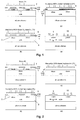
- the first non-standard devices are NP1N and PP2P MOS transistors. They may be obtained by means of a mask arrangement as shown in fig. 1. Two masks are used, a p-channel-exposure mask 1 and an n-channel-exposure mask 2.
- the p-channel-exposure mask when opaque, protects the active silicon area 3 against the ion implantation 5 relative to standard inversion mode n-MOS transistor channel doping.
- the n-channel-exposure mask 2 does the same with the active silicon area for the ion implantation 6 relative to standard accumulation mode p-MOS transistors.
- All n-MOS devices have to be treated against edge effects which create leak currents. Two strategies are possible to avoid such edge effect.
- the first one is based on edgeless transistors.
- a second strategy consists in changing the doping near the transistor edges. This solution is more difficult to implement than the first one, but it has to be used if the transistor geometry is such that the gate length is similar or higher than the gate width. This kind of sizing is conventional for very low-power analog circuits where weak inversion is usually required.
- edgeless transistors are by large boron implantation in n-MOS oxide edges. For p-MOS it is the opposite. None of them can receive boron implantation near their silicon edges, otherwise a resistive lateral path would be open between source and drain, leading to a large leakage current.
- a boron dose 7 is implanted along the oxide 8 surrounding the n-MOS transistor active area 3.
- the p-channel-exposure mask 1 is thereby used to define areas where boron 7 will not be implanted along the field oxide 8 (fig. 1(a)).
- the p-channel-exposure mask 1 is thereafter used for carrying out the standard n-MOS channel implementation P2 (fig. 1 (b)).
- This p-channel-exposure mask 1 in order to obtain the non-standard devices NP1N and PP2P, shields what will be the p-MOS transistor, and allows the n-MOS channel implantation at what will be the n-MOS transistor. N-MOS transistor edges receive a first P2 doping level.
- the n-channel-exposure mask 2 is used for carrying out the standard p-MOS channel implantation P1 (fig. 1(c)).
- This n-channel-exposure mask 2 in order to obtain the non-standard devices NP1N and PP2P, shields what will be the n-MOS transistor, and allows the p-MOS channel implantation at what will be the p-MOS transistor.
- the resulting CMOS devices are shown in fig. 1 (d), with the resulting n-MOS transistor 9 at the left of fig. 1(d) and the resulting p-MOS transistor 10 at the right of fig. 1(d).
- the p-channel-exposure mask 1 and the n-channel-exposure mask 2 are geometrically complementary.
- the p-channel-exposure mask 1 and the n-channel-exposure mask 2 are not complementary anymore.
- the new n-MOS transistor 9 of type NP1N takes advantage of the standard p-MOS device doping level, while the new p-MOS transistor 10 of type PP2P takes advantage of the standard n-MOS device doping level.
- n-MOS doping level
- P1 and P2 doping level
- P12 doping level
- Devices such as NP12N and PP12P can therefore be implemented.
- Fig. 2 presents simplified process steps relative to NP12N and PP12P devices.
- the n-MOS device is processed in order to avoid edge effect. Therefore, a boron dose 7 is implanted along the oxide 8 surrounding the n-MOS transistor active area 11 by using a p-channel-exposure mask 1, as can be seen in fig. 2 (a).
- the p-channel-exposure mask 1 is thereafter used again for carrying out the ion implantation 5 relative to standard inversion mode n-MOS transistors channel doping (P2) (fig. 2 (b)).
- P2 standard inversion mode n-MOS transistors channel doping
- the whole n-MOS transistor and the channel area of the p-MOS transistor receive this ion implantation 5.
- No mask is used when carrying out the ion implantation 6 relative to standard inversion mode p-MOS transistor channel doping (P1), so that the whole n-MOS transistor as well as the whole p-MOS transistor get this implantation (fig. 2 (c)).
- the resulting CMOS devices are shown in fig. 2 (d), with the resulting n-MOS transistor 9 at the left of fig. 2 (d) and the resulting p-MOS transistor 10 at the right of fig. 2 (d).
- CMOS devices without any channel doping implantation can be implemented (fig. 3).
- NIN and PIP with "I" standing for an intrinsic region even if in practice, SOI wafers provided by industry are not intrinsic but are usually slightly p-type doped).
- the acceptor doping concentration may be approximately 1x 10 15 atoms/cm 3 .
- a p-channel-exposure mask 1 is used to define areas where boron will not be implanted along the field oxide 8, so that boron is only implanted along the oxide 8 surrounding the n-MOS transistor active area 11 (fig. 3 (a)).
- the same p-channel-exposure mask 1 is used in a second step for carrying out an ion implantation 5 relative to standard n-MOS channel doping implementation P2 (fig. 3 (b)).
- This p-channel-exposure mask 1 only allows the implantation to be carried out at the edge regions of the n-MOS transistor.
- An n-channel-exposure mask 2 blocks every ion implantation 6 relative to standard p-MOS transistor channel doping (P2) (fig. 3(c)).
- the resulting CMOS devices are shown in fig. 3 (d), with the resulting n-MOS transistor 9 at the left of fig. 3 (d) and the resulting p-MOS transistor 10 at the right of fig. 3 (d).
- the doping profile of the n-MOS transistor 9 is not uniform over the transistor width as it requires edge effect lateral implementation.
- an additional mask may be used to implant an n-type channel ion implantation (doping level called N).
- N n-type channel ion implantation
- CMOS devices such a mask allows to implement two new transistors, called NNN and PNP.
- NNN and PNP devices are implemented at first exactly like NIN and PIP devices respectively. Selected intrinsic devices are then implanted on an additional process step with the "N" doping level mask.
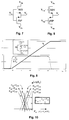
- the threshold voltage for a fully depleted n-MOSFET working in inversion mode is given by: whereby
- any other combination of n-MOS and p-MOS transistors whereby the absolute values of the threshold voltages of both transistors are different and whereby the absolute value of the relative difference of the threshold voltages of the two transistors is between 0.9 and 1.3 Volts, can be used for the basic cell according to the present invention.
- Threshold voltages for intrinsic n- and p-MOSFET are about -0.3V and -0.8V respectively.
- the intersection of these curves is characterised by a gate to source voltage close to -0.55 V and a current about 10 pA at room temperature for the given transistor aspect ratio.
- sub-threshold slopes are modified as well as both n and p-MOS threshold voltages. Supposing that both temperature coefficients for V th-n and V th-p are identical (absolute value) and that both sub-threshold slopes evolve similarly, then the intersection locus of the curves of fig. 5 will go to higher current with increasing temperature, but the crossover gate to source voltage (V G0 ) will remain close to -0.55V.
- V G0 constant voltage
- an n-MOS transistor and a p-MOS transistor are connected with both their gates and sources together, as can be seen in fig. 7. Generally, both gates need not be connected together as will be described in a more general basic block below.
- This first architecture integrates two basic functions, i.e. a basic level shifter (between V G and V S ) and an ultra-low current source able to push and/or pull current (double current source) depending on the considered access node (V Dn or V Dp ).
- the voltage shift is not very sensitive to temperature, while the current source value is strongly (exponentially) dependent on the temperature, as shown in fig. 6.
- the current source property comes from the fact that both drain voltages have virtually no influence on the source voltage as long as devices are saturated. Therefore V GS is independent of drain voltages, which means that current flowing towards both devices is constant at a fixed temperature. If the temperature increases the current increase has an exponential dependence as the device works in weak inversion and is polarised at constant V GS .
- This basic cell of this embodiment can be considered as a "floating" one (independent of V Dn and V Dp ) if previous conditions are respected.
- the source voltage V S follows the applied gate voltage V G .
- the substrate effect also called back gate effect
- the substrate effect will only depend on the (common) source voltage.
- Id-Vg curves are shifted, as transistor threshold voltages are correlated to V BS with the substrate effect factor ⁇ .
- ⁇ may be close to 0.08 for both n-MOS and p-MOS transistors. This means that if V S increases, then V BS decreases and both curves of fig. 5 are shifted to the right by ⁇ .V BS . Therefore, the intersection of the curves is also shifted to the right by ⁇ .V BS . Due to this effect, the source voltage V S will not exactly follow the gate voltage V G with a constant offset.
- Fig. 8 shows the simulation result of the basic architecture with the back gate tied to the ground.
- source voltage V S "follows" gate voltage V G with a coefficient 1/(1+ ⁇ ) as long as both transistors are saturated.
- U T I Dp I Sp ( T ).
- U T is the thermal voltage defined as kT/q.
- V S V B ( ⁇ -1)+ V G - V G 0 ⁇
- the basic architecture of fig. 7 can also be used as a voltage reference. Based on fig. 4 and equation eq. 2, one can fix a V S value for a given V G value.
- V G For N, I and P1 channel doping levels, if V G is tied to ground, the obtained reference voltages are respectively 1.04, 0.49 and 0.3 V. For P2 and P12 doping levels, V G has to be connected to a positive voltage to ensure saturation mode. If V G is tied to the supply voltage V DD , then the output voltages are V DD 1.08 -(0.21;0.41) Volts respectively. As mentioned previously, all these voltages are few sensitive to temperature.
- n- and p-MOS devices have the same size.
- a reference voltage with some temperature dependence.
- Such a voltage could, for example, compensate, at first order, the gate to source voltage variation at constant drain current of a MOS transistor in weak inversion in order to get a low level current source less sensitive to temperature.
- Fig. 12 represents the simulated reference voltage dependence over temperature for various size ratios ⁇ .
- the lower curve corresponds to an n-MOS device being 1000 times wider than the p-MOS device
- the upper curve corresponds to an p-MOS device being 1000 times wider than the n-MOS device. It is to be noted that, if the size ratio is too high, it is difficult to keep both devices in weak inversion.
- the new configuration may be interpreted as exhibited in fig. 10.
- V Gp and V Gn respectively decrease and increase while the common mode stays constant (dashed lines), then the intersection still occurs at a same voltage level while the current value exponentially increases. If the common mode voltage is not constant, then the crossing point of n- and p-MOS Id-Vg curves is shifted due to the substrate effect as explained before.
- the functionality of this generalised basic block is therefore similar to a floating differential transconductance amplifier, where the output current is also precisely defined by the differential input voltage.
- fig. 11 compares the new proposed generalised block (a) with a usual differential transconductance architecture (b). The difference between both is that in the new proposed transconductance of fig. 11 a current source is not necessary.
- the output current is not limited, it depends exponentially on the input voltage; where in the usual differential transconductance of fig. 11b, the output current is limited by the bias current source I 0 .
- All basic cells can be horizontally cascaded as depicted in fig. 13. This allows some more intermediate values of reference voltages to be obtained.
- two common gate basic cells are horizontally cascaded, whereby the output node V S1 of the first basic cell is connected to the input node V G of the second basic cell.
- V S1 a voltage of 0.49V with transistors of the FD-SOI CMOS process previously mentioned. This voltage is the gate voltage for the next stage.
- V S2 would be lower than V S1 (as V G0 is larger in that case, as can be seen in fig. 4). In all cases of basic cells with different doping levels being cascaded, it has to be verified that all the transistors remain saturated.
- Such cascade of basic cells also allows addition of a temperature dependence of each basic cell in order to increase the sensitivity of the output voltage versus a temperature variation by using basic cells with different size ratios.
- the drain of the n-MOS transistor of the first basic cell is connected to the drain of the p-MOS transistor of the second basic cell.
- the output node V S1 of the first basic cell is connected to the common gate of the second basic cell.
- Diode like characteristics are required in some typical applications, such as charge pump voltage multipliers or rectifiers.
- Fig. 15 shows different implementations of diodes.
- the first diode mentioned is a conventional pn-junction diode.
- the second diode mentioned is a prior art MOS diode architecture, which is a MOSFET with its gate connected to its drain. I S is the saturation current for the standard MOS diode (n or p-MOS).
- the third diode mentioned is a diode according to an embodiment of the present invention.
- diode current curve is set out on a linear scale, a plot as in fig. 16b is obtained.
- a negative diode impedance is obtained on some voltage range of the reversed biased diode. This negative impedance means that, for slightly reverse currents, there are two different possible stable voltages.
- the basic architecture of a charge pump voltage doubler is given in fig. 17. It comprises two diodes, D 1 and D 2 , coupled in series between a voltage source V DD and a load capacitance C L (usually a MOSFET gate). At the node between both diodes D 1 and D 2 , a capacitance C 1 is connected, which is connected with its other node to a clock CK, which is a step function switching between V DD and 0 V. V out is the voltage over the load capacitance C L .
- both diodes D 1 and D 2 are standard n-MOS diodes, then after a transient period, the output voltage on the load capacitance C L is expected to be 2.V DD . However, due to losses, V out is lower than 2.V DD and presents ripples, as can be seen on fig. 18.
- voltage V 1 is basically the input clock signal clamped to V DD . This means that the diode D 1 is polarised either with a voltage close to 0 or to a negative voltage (-V DD ). When D 1 is reverse biased, capacitor C 1 slightly discharges due to the diode reverse leakage current. Similar conclusions can be found for the output diode D 2 .
- diodes are no longer strongly biased. This means that forward currents are very small. In fact, these MOS diodes work only in weak inversion for such current level. It is to be noted that all previous considerations are valid only for a capacitive load at the output voltage (a resistive load would lead to higher forward current peaks in diodes). The usual concept of "diode threshold" has no significance anymore in the present case. Considering the following MOS diode current-voltage relation in weak inversion, the critical parameter is I S , the saturation current which depends on the channel doping level and on the MOS diode size. During the steady state, at each moment, either diode D 1 or D 2 is reverse biased by approximately V DD .
- the corresponding reverse current corresponds to energy loss on each clock cycle.
- the output capacitance is charged through diode D 2 in order to compensate previous mentioned loss.
- the charge transfer from C 1 to C L half the energy is lost by the corresponding loop impedance, whatever the impedance value. The impedance will only affect the charge transfer speed.
- Another energy loss source is related to the parasitic capacitance (C P ) to ground at the common node between both diodes.
- C P parasitic capacitance
- the internal node only increases by (V DD .C 1 )/(C 1 +C P ).
- the theoretical maximum output voltage is therefore This means that the MOS diodes should be as small as possible in order to minimise C P . It can be concluded that, for prior art CMOS diodes, the output voltage value is close to optimum with a short settling time if the saturation current I S is high and if the diode capacitance to ground is small. This however is achieved at the cost of a large ripple on the output voltage.
- static memory used for example in random access memories (RAM).
- RAM random access memories
- the simplest way to implement such static memory is to use two cross-coupled inverters with the input of one being the output of the other one.
- Two pass transistors, Word_line 1 and Word_line 2 are used to symmetrically impose the static memory steady state (i.e. write 1 or 0). This is represented in fig. 19.
- the static consumption of such basic cell is due to the off-state current of each inverter, i.e. drain to source current when the gate to source voltage is zero. This value depends on MOSFET threshold voltages.
- This last power loss is due to the current flowing through both inverters when they change their states.
- a second loss during the write transient is due to the fact that in order to change the state of the memory, the driver which has to change the state of the memory has to be "stronger” than both inverters of the memory cell whereas during the "read” operation, the inverters must be strong enough to drive the bus lines.
- Fig. 20 (a) represents the basic ULP memory cell architecture according to the present invention.
- Fig. 20 (b) represents the current difference between the upper and the lower ULP diodes (D 1 and D 2 ) respectively versus the voltage level (V ram ) of the memory cell.
- the plotted current difference is based on the weak inversion (wi) relation only.
- V ram is below V DD /2
- the current difference I D1 -I D2 is negative. This means that the node capacitance C will be discharged down to a value close to zero volt. If V ram is above V DD /2, the node will be charged up to a value close to V DD (because I D1 -I D2 is positive).
- Such an architecture is therefore auto-regenerative for both logical levels "0" and "1".
- the main advantage is the absence of a feedback loop, as for the standard architecture of fig. 19. Furthermore, the static current consumption of the architecture according to the present invention is lower than the usual one, because the reverse biased ULP diodes have less leakage current than prior art diodes.
- the regeneration current level of the memory cell architecture depends on saturation currents (I S ), i.e. on the threshold voltage of both n- and p-MOSFETs.
- I S saturation currents
- n-MOSFETs with threshold voltages close to zero or even negative
- k is a numeric representation of the disymmetry between n-MOSFET and p-MOSFETs threshold voltage of fig. 4).
- the memory cell architecture according to this embodiment of the present invention is not suited for high voltage supply. Indeed, in such cases the regeneration current becomes very small when V ram is close to V DD /2 as can be seen on fig. 21, where the regeneration current is given in function of the voltage level of the memory cell in case the supply voltage V DD equals 2 Volts.
- the lower supply voltage limit has to be higher than two times the diode voltage corresponding to the higher reverse current.
- this ULP memory cell can work down to 0.5 V of supply voltage. It is to be noted that decreasing the supply voltage means increasing the ULP memory cell consumption, as ULP diodes are not strongly reverse biased.
- the new memory cell architecture presents significant advantages (consumption and speed) compared to standard architectures for low voltage and/or high temperature RAM.
- This basic memory cell associated with pass gates, can also be used for other digital circuits, such as D and master-slave flip-flops.
- Electrostatic Discharge (ESD) protection is a key element for industrial processes.
- An electrostatic discharge is a transfer of electrostatic charge between two bodies at different electrostatic potentials caused by direct contact or induced by an electrostatic field.
- a charge static electricity
- the static electricity can damage or degrade electronic components, therefore integrated circuits have to resist electrostatic stress in harsh industrial environments or on human hand contact.
- One discharge in the wrong place can destroy expensive circuits and cause errors, "down time” and production delays.
- the proposed ULP ESD solution of the present invention is to use the ULP diode of the present invention with a high saturation current in order to implement diodes D 1 and D 2 . This allows a large forward current while keeping a low leakage current in normal regime.
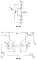
- a ULP operational transconductance amplifier (OTA) is implemented, the basic architecture of which is depicted in fig. 23. It comprises 4 transistors M1, M2, M3, M4. Transistors M1 and M2 act like an ULP differential transconductance while MOSFETs M3 and M4 are used as a ULP current source.
- OTA operational transconductance amplifier
- V0 gm diff I .
- the ULP OTA offset is the input differential voltage that should be applied in order to equalize the current of the upper current source with the current of the differential pair.
- the offset would be zero if substrate effects and matching were neglected. If all devices work in weak inversion (which is the case in the example given), a current difference between the upper and the lower part of fig.
- fig. 4 shows that the intersection of n- and p-MOSFETs IdVg curves for the same channel doping does not occur exactly at a same current level for each doping dose. For a well characterised process, it is possible to compensate this current difference by an adequate sizing of each of the devices in order to reduce the OTA systematic offset.
- the input common mode upper limit also depends on the upper current source of fig. 23.
- the current source in fig. 23 only P2 and P12 channel doping can be used in order to ensure saturation of transistor M4.
- transistors M1 and M2 channels were doped at a level P12 of P2 and if transistor M3 and M4 are still P2 doped, then the minimum and the maximum common mode voltage would be both about 200 mV higher (based on the values previously calculated).
- the input common mode can reach V DD .
- the table hereinafter summarises the common mode range of the OTA of fig. 23 as a function of the differential transconductance doping level (I, P1, P2 or P12) with an upper current source doped at a P2 level.
- Fig. 25 represents a rail to rail (input and output) ULP OTA architecture.
- the input rail to rail is achieved thanks to two differently doped differential transconductances in parallel (P12 and I type in the example given).
- P12 and I type in the example given For an input common mode voltage range far from V DD and V SS , both input transconductances work in parallel.
- I doping level in the example given For an input common mode voltage close to V SS , only the weakly P type doped transconductance will be active (I doping level in the example given), the other being strongly desaturated. In the other case of high input common mode voltage, only the strongly P type doped transconductance will be active (P12 doping level in the example given).
- the gain is only weakly dependent on the input common mode value.
- the overall amplifier current consumption at room temperature is about 5pA.
- the leakage current level has to be much lower than the amplifier current consumption. This will be the case if the n- and p-MOSFET intersection (for the same channel doping) of fig. 4 happens at a sufficiently higher current level than the devices leakage current level.
- CMRR common mode rejection ratio
- the ULP architecture does not limit the output current versus the differential input voltage (this is based on fig. 11(a) - current dependent on voltage).
- a dynamic threshold MOS (DTMOS) transistor comprises a MOS transistor of which the substrate is connected to the gate of the transistor. Given the fact that the threshold voltage of a MOS transistor decreases more as the substrate is positively polarised, the DTMOS transistor has a threshold voltage which decreases by increasing the gate to source voltage of the transistor. This results in a quicker transition from the non-conducting to the conducting mode of the transistor.
- a disadvantage of this type of transistors is that as from a gate to source tension in the order of 0.5 - 0.6 V, the substrate current is not negligible anymore, as the diode formed between substrate and source becomes current conducting. This current strongly deteriorates the input impedance of the transistor.
- a diode according to the present invention is introduced between the gate and the substrate contact, as shown in fig. 26.
- the current characteristic in function of the voltage over the diode, as shown in fig. 16b shows that, with relation to the new DTMOS device with ULP diode, the input current will be limited as from a certain input voltage. Indeed, if at first V GS is zero and is augmented, the substrate will first be current conducting (which current is negligible - in the order of ⁇ A) which allows a good polarisation of the substrate (diode slightly reversed biased). Thereafter, as the gate to source voltage V GS increases, less and less current will pass through the diode, and will quickly limit the substrate current.
- An optimisation of the doping levels used in the diode allows the regulation of the maximum bulk current of the transistor.
- n- and p-MOS transistors are used, also n- and p-MOS transistors with other channel doping levels may be used.
- SOI MOS process is used for obtaining specific transistors; if other processes are used, other values may be found for each of the variables calculated hereinabove.
Priority Applications (5)
| Application Number | Priority Date | Filing Date | Title |
|---|---|---|---|
| EP00870313A EP1217662A1 (fr) | 2000-12-21 | 2000-12-21 | Blocs élémentaires d'ultra-faible puissance et leurs utilisations |
| AU2002233277A AU2002233277A1 (en) | 2000-12-21 | 2001-12-17 | Ultra-low power basic blocks and their uses |
| PCT/EP2001/015023 WO2002050911A1 (fr) | 2000-12-21 | 2001-12-17 | Blocs-cylindres a tres faible consommation d'energie et leurs utilisations |
| EP01984867A EP1344253A1 (fr) | 2000-12-21 | 2001-12-17 | Blocs-cylindres a tres faible consommation d'energie et leurs utilisations |
| US10/602,016 US6870229B2 (en) | 2000-12-21 | 2003-06-23 | Ultra-low power basic blocks and their uses |
Applications Claiming Priority (1)
| Application Number | Priority Date | Filing Date | Title |
|---|---|---|---|
| EP00870313A EP1217662A1 (fr) | 2000-12-21 | 2000-12-21 | Blocs élémentaires d'ultra-faible puissance et leurs utilisations |
Publications (1)
| Publication Number | Publication Date |
|---|---|
| EP1217662A1 true EP1217662A1 (fr) | 2002-06-26 |
Family
ID=8175884
Family Applications (2)
| Application Number | Title | Priority Date | Filing Date |
|---|---|---|---|
| EP00870313A Withdrawn EP1217662A1 (fr) | 2000-12-21 | 2000-12-21 | Blocs élémentaires d'ultra-faible puissance et leurs utilisations |
| EP01984867A Withdrawn EP1344253A1 (fr) | 2000-12-21 | 2001-12-17 | Blocs-cylindres a tres faible consommation d'energie et leurs utilisations |
Family Applications After (1)
| Application Number | Title | Priority Date | Filing Date |
|---|---|---|---|
| EP01984867A Withdrawn EP1344253A1 (fr) | 2000-12-21 | 2001-12-17 | Blocs-cylindres a tres faible consommation d'energie et leurs utilisations |
Country Status (4)
| Country | Link |
|---|---|
| US (1) | US6870229B2 (fr) |
| EP (2) | EP1217662A1 (fr) |
| AU (1) | AU2002233277A1 (fr) |
| WO (1) | WO2002050911A1 (fr) |
Cited By (1)
| Publication number | Priority date | Publication date | Assignee | Title |
|---|---|---|---|---|
| EP1398836A3 (fr) * | 2002-09-10 | 2006-09-27 | Nec Corporation | Dispositif semiconducteur à couche mince et son procédé de fabrication |
Families Citing this family (20)
| Publication number | Priority date | Publication date | Assignee | Title |
|---|---|---|---|---|
| SG104264A1 (en) * | 2000-02-10 | 2004-06-21 | Matsushita Electric Ind Co Ltd | Lens, manufacturing method thereof, and optical device using the same lens |
| US6724655B2 (en) * | 2000-06-22 | 2004-04-20 | Progressant Technologies, Inc. | Memory cell using negative differential resistance field effect transistors |
| US20110026323A1 (en) | 2009-07-30 | 2011-02-03 | International Business Machines Corporation | Gated Diode Memory Cells |
| US8445946B2 (en) * | 2003-12-11 | 2013-05-21 | International Business Machines Corporation | Gated diode memory cells |
| JP4114751B2 (ja) * | 2004-03-31 | 2008-07-09 | シャープ株式会社 | 半導体装置 |
| TWI242404B (en) * | 2004-07-22 | 2005-10-21 | Hannstar Display Corp | A display device and protection circuits thereof |
| US7957110B2 (en) * | 2005-01-25 | 2011-06-07 | Hannstar Display Corporation | Display apparatus current discharging method |
| EP1917715A2 (fr) * | 2005-07-22 | 2008-05-07 | Nanopower Technologies, Inc. | Circuits integres d'etiquette rfid a sensibilite elevee |
| DE102005055224A1 (de) * | 2005-11-19 | 2007-05-24 | Lübcke, Armin | Abfalleimer mit Vakuumerzeugung |
| US20090122451A1 (en) * | 2007-11-08 | 2009-05-14 | Meng-Yong Lin | Esd protection circuit device |
| JP2010011158A (ja) * | 2008-06-27 | 2010-01-14 | Fujifilm Corp | 検出素子 |
| US8441307B2 (en) * | 2009-09-01 | 2013-05-14 | Aptus Power Semiconductor | Methods and circuits for a low input voltage charge pump |
| US8957732B2 (en) | 2010-05-25 | 2015-02-17 | Agency For Science, Technology And Research | Amplifier and transceiver including the amplifier |
| US8837188B1 (en) | 2011-06-23 | 2014-09-16 | Netlogic Microsystems, Inc. | Content addressable memory row having virtual ground and charge sharing |
| US8773880B2 (en) | 2011-06-23 | 2014-07-08 | Netlogic Microsystems, Inc. | Content addressable memory array having virtual ground nodes |
| US9337840B2 (en) * | 2013-05-17 | 2016-05-10 | Samsung Electronics Co., Ltd. | Voltage level shifter and systems implementing the same |
| US9608437B2 (en) * | 2013-09-12 | 2017-03-28 | Qualcomm Incorporated | Electro-static discharge protection for integrated circuits |
| FR3057104A1 (fr) * | 2016-10-04 | 2018-04-06 | Commissariat A L'energie Atomique Et Aux Energies Alternatives | Transistors a effet de champ de type fdsoi |
| US10236768B2 (en) | 2017-05-19 | 2019-03-19 | Globalfoundaries Inc. | Switched-capacitor charge pump with reduced diode threshold voltage and on state resistance |
| US10855170B2 (en) | 2017-06-22 | 2020-12-01 | E-Peas S.A. | Power management integrated circuit with programmable cold start |
Citations (8)
| Publication number | Priority date | Publication date | Assignee | Title |
|---|---|---|---|---|
| JPS60246418A (ja) * | 1984-05-22 | 1985-12-06 | Nec Corp | 基準電位発生回路 |
| US4860257A (en) * | 1986-11-30 | 1989-08-22 | Samsung Semiconductor And Telecommunications Co., Ltd. | Level shifter for an input/output bus in a CMOS dynamic ram |
| US4990847A (en) * | 1988-12-19 | 1991-02-05 | Mitsubishi Denki Kabushiki Kaisha | Microcomputer |
| EP0653843A2 (fr) * | 1993-11-17 | 1995-05-17 | Hewlett-Packard Company | Circuits CMOS à seuil de tension adaptatif |
| JPH07240470A (ja) * | 1994-02-25 | 1995-09-12 | Toshiba Corp | 半導体装置 |
| US5463348A (en) * | 1994-07-27 | 1995-10-31 | California Institute Of Technology | CMOS low-power, wide-linear-range, well-input differential and transconductance amplifiers |
| US5506527A (en) * | 1994-04-15 | 1996-04-09 | Hewlett-Packard Compnay | Low power diode |
| US6031403A (en) * | 1996-11-13 | 2000-02-29 | International Business Machines Corporation | Pull-up and pull-down circuits |
Family Cites Families (4)
| Publication number | Priority date | Publication date | Assignee | Title |
|---|---|---|---|---|
| KR100242997B1 (ko) * | 1996-12-30 | 2000-02-01 | 김영환 | 저전력 소비 입력 버퍼 |
| JP4253052B2 (ja) * | 1997-04-08 | 2009-04-08 | 株式会社東芝 | 半導体装置 |
| JP2959528B2 (ja) * | 1997-06-09 | 1999-10-06 | 日本電気株式会社 | 保護回路 |
| US6069782A (en) * | 1998-08-26 | 2000-05-30 | Integrated Device Technology, Inc. | ESD damage protection using a clamp circuit |
-
2000
- 2000-12-21 EP EP00870313A patent/EP1217662A1/fr not_active Withdrawn
-
2001
- 2001-12-17 EP EP01984867A patent/EP1344253A1/fr not_active Withdrawn
- 2001-12-17 WO PCT/EP2001/015023 patent/WO2002050911A1/fr not_active Application Discontinuation
- 2001-12-17 AU AU2002233277A patent/AU2002233277A1/en not_active Abandoned
-
2003
- 2003-06-23 US US10/602,016 patent/US6870229B2/en not_active Expired - Lifetime
Patent Citations (8)
| Publication number | Priority date | Publication date | Assignee | Title |
|---|---|---|---|---|
| JPS60246418A (ja) * | 1984-05-22 | 1985-12-06 | Nec Corp | 基準電位発生回路 |
| US4860257A (en) * | 1986-11-30 | 1989-08-22 | Samsung Semiconductor And Telecommunications Co., Ltd. | Level shifter for an input/output bus in a CMOS dynamic ram |
| US4990847A (en) * | 1988-12-19 | 1991-02-05 | Mitsubishi Denki Kabushiki Kaisha | Microcomputer |
| EP0653843A2 (fr) * | 1993-11-17 | 1995-05-17 | Hewlett-Packard Company | Circuits CMOS à seuil de tension adaptatif |
| JPH07240470A (ja) * | 1994-02-25 | 1995-09-12 | Toshiba Corp | 半導体装置 |
| US5506527A (en) * | 1994-04-15 | 1996-04-09 | Hewlett-Packard Compnay | Low power diode |
| US5463348A (en) * | 1994-07-27 | 1995-10-31 | California Institute Of Technology | CMOS low-power, wide-linear-range, well-input differential and transconductance amplifiers |
| US6031403A (en) * | 1996-11-13 | 2000-02-29 | International Business Machines Corporation | Pull-up and pull-down circuits |
Non-Patent Citations (2)
| Title |
|---|
| PATENT ABSTRACTS OF JAPAN vol. 010, no. 116 (P - 452) 30 April 1986 (1986-04-30) * |
| PATENT ABSTRACTS OF JAPAN vol. 1996, no. 01 31 January 1996 (1996-01-31) * |
Cited By (5)
| Publication number | Priority date | Publication date | Assignee | Title |
|---|---|---|---|---|
| EP1398836A3 (fr) * | 2002-09-10 | 2006-09-27 | Nec Corporation | Dispositif semiconducteur à couche mince et son procédé de fabrication |
| US7224224B2 (en) | 2002-09-10 | 2007-05-29 | Nec Corporation | Thin film semiconductor device and manufacturing method |
| EP1873786A2 (fr) * | 2002-09-10 | 2008-01-02 | NEC Corporation | Dispositif d'imagerie à infrarouge de type thermique et son procédé de fonctionnement |
| US7595533B2 (en) | 2002-09-10 | 2009-09-29 | Nec Corporation | Thin film semiconductor device and manufacturing method |
| EP1873786A3 (fr) * | 2002-09-10 | 2015-01-14 | Gold Charm Limited | Dispositif d'imagerie à infrarouge de type thermique et son procédé de fonctionnement |
Also Published As
| Publication number | Publication date |
|---|---|
| US6870229B2 (en) | 2005-03-22 |
| EP1344253A1 (fr) | 2003-09-17 |
| WO2002050911A1 (fr) | 2002-06-27 |
| AU2002233277A1 (en) | 2002-07-01 |
| US20040026760A1 (en) | 2004-02-12 |
Similar Documents
| Publication | Publication Date | Title |
|---|---|---|
| EP1217662A1 (fr) | Blocs élémentaires d'ultra-faible puissance et leurs utilisations | |
| KR100288818B1 (ko) | 반도체 집적회로 | |
| US5557231A (en) | Semiconductor device with improved substrate bias voltage generating circuit | |
| JP3633061B2 (ja) | 半導体集積回路装置 | |
| US8120386B2 (en) | Amplifiers using gated diodes | |
| US5838189A (en) | Substrate voltage generating circuit of semiconductor memory device | |
| US6677803B1 (en) | Semiconductor integrated circuit device | |
| US20110057705A1 (en) | Semiconductor apparatus and breakdown voltage control method of the same | |
| US9837439B1 (en) | Compensation of temperature effects in semiconductor device structures | |
| US6628161B2 (en) | Reference voltage circuit | |
| US20040090820A1 (en) | Low standby power SRAM | |
| US7906800B2 (en) | Semiconductor integrated circuit | |
| KR980012291A (ko) | 반도체 장치 | |
| US7728386B2 (en) | Semiconductor integrated circuit device | |
| KR0137857B1 (ko) | 반도체 장치 | |
| US6636073B2 (en) | Semiconductor integrated circuit | |
| US7078953B2 (en) | Level down converter | |
| US11616506B2 (en) | High speed buffer circuit | |
| WO1999026334A1 (fr) | Montage amplificateur oscillant et basse tension, et dispositif electronique portatif incorporant ce montage | |
| US6891419B2 (en) | Methods and apparatus for employing feedback body control in cross-coupled inverters | |
| Aggarwal et al. | Low-voltage cascode current mirror based on bulk-driven MOSFET and FGMOS techniques | |
| US6271706B1 (en) | Divided voltage de-coupling structure | |
| US20070267702A1 (en) | Dynamic threshold P-channel MOSFET for ultra-low voltage ultra-low power applications | |
| US20190302823A1 (en) | Constant current circuit, semiconductor device, electronic apparatus, and method of manufacturing semiconductor device | |
| US5936290A (en) | Semiconductor device having an insulated gate field effect transistor and a well spaced from the channel region of the insulated gate field effect transistor |
Legal Events
| Date | Code | Title | Description |
|---|---|---|---|
| PUAI | Public reference made under article 153(3) epc to a published international application that has entered the european phase |
Free format text: ORIGINAL CODE: 0009012 |
|
| AK | Designated contracting states |
Kind code of ref document: A1 Designated state(s): AT BE CH CY DE DK ES FI FR GB GR IE IT LI LU MC NL PT SE TR |
|
| AX | Request for extension of the european patent |
Free format text: AL;LT;LV;MK;RO;SI |
|
| AKX | Designation fees paid |
Designated state(s): BE |
|
| REG | Reference to a national code |
Ref country code: DE Ref legal event code: 8566 |
|
| STAA | Information on the status of an ep patent application or granted ep patent |
Free format text: STATUS: THE APPLICATION IS DEEMED TO BE WITHDRAWN |
|
| 18D | Application deemed to be withdrawn |
Effective date: 20021228 |