EP1217522A2 - Watchdog timer and method for detecting abnormal operation of computer, and computer including the timer - Google Patents
Watchdog timer and method for detecting abnormal operation of computer, and computer including the timer Download PDFInfo
- Publication number
- EP1217522A2 EP1217522A2 EP01130680A EP01130680A EP1217522A2 EP 1217522 A2 EP1217522 A2 EP 1217522A2 EP 01130680 A EP01130680 A EP 01130680A EP 01130680 A EP01130680 A EP 01130680A EP 1217522 A2 EP1217522 A2 EP 1217522A2
- Authority
- EP
- European Patent Office
- Prior art keywords
- signal
- timer
- mode
- circuit
- reset
- Prior art date
- Legal status (The legal status is an assumption and is not a legal conclusion. Google has not performed a legal analysis and makes no representation as to the accuracy of the status listed.)
- Withdrawn
Links
Images




Classifications
-
- G—PHYSICS
- G06—COMPUTING OR CALCULATING; COUNTING
- G06F—ELECTRIC DIGITAL DATA PROCESSING
- G06F11/00—Error detection; Error correction; Monitoring
- G06F11/30—Monitoring
-
- G—PHYSICS
- G06—COMPUTING OR CALCULATING; COUNTING
- G06F—ELECTRIC DIGITAL DATA PROCESSING
- G06F11/00—Error detection; Error correction; Monitoring
- G06F11/07—Responding to the occurrence of a fault, e.g. fault tolerance
- G06F11/0703—Error or fault processing not based on redundancy, i.e. by taking additional measures to deal with the error or fault not making use of redundancy in operation, in hardware, or in data representation
- G06F11/0751—Error or fault detection not based on redundancy
- G06F11/0754—Error or fault detection not based on redundancy by exceeding limits
- G06F11/0757—Error or fault detection not based on redundancy by exceeding limits by exceeding a time limit, i.e. time-out, e.g. watchdogs
Definitions
- the present invention relates to a watchdog timer and method for detecting abnormal operations of a computer.
- the present invention relates also to a computer including the watchdog timer for detecting abnormal operations of the computer.
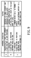
- Computers may operate out of control or stop operating as a result of any of various factors, as described in FIG. 9.
- Disclosed in Unexamined Japanese Patent Application KOKAI Publication No. S61-62947 is a method, employing a timer, for detecting such abnormal operations of computers and setting the computers back into a normal state.
- the timer begins operating in accordance with commands of a software program for controlling a computer.
- the watchdog timer counts pulses of a clock, and the counted value is cleared at predetermined intervals under the control of the software program.
- the counted value exceeds a predetermined limit value instead of being cleared.
- the watchdog timer controls the computer to execute a reset process.
- the watchdog timer begins operating by the commands of the software program. Hence, the abnormal operation occurring during the activation of the software program can not satisfactorily be detected.
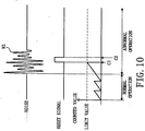
- the computer is operated out of control, and the counted value reaches the limit value (C1). Hence, the computer is reset by the watchdog timer, and begins the reset process (C2). However, the noise N1 still remains at the time of beginning the reset process, the computer is again operated out of control. Thus, the software program is not activated, and the watchdog timer does not operate, either.
- the conventional watchdog timer can not detect the abnormal operations occurring in the computer during the activation of the software program.
- the computer can not be employed for any apparatuses which do not need the functions of the watchdog timer. In other words, any of those computers each including the watchdog timer can not be used for various purposes.
- the present invention has been made in consideration of the above. It is accordingly an object of the present invention to provide a watchdog timer which can be used for various purposes.
- Another object thereof is to provide a watchdog timer and method for reliably detecting abnormal operations of computers.
- Still another object thereof is to provide a computer including the watchdog timer reliably detecting the abnormal operations of the computers.
- a computer comprising:
- the timer (10, 30) may have a plurality of operational modes.
- the controller (1) may output a mode specification signal (103, 104) for specifying an operational mode of the timer (10, 30), to the timer (10, 30); and the timer (10,30) may set an operational mode thereof, in accordance with the mode specification signal (103, 104).
- the timer (10, 30) may include a circuit, which sets the mode specification signal (104) sent from the controller (1) ineffective in response to setting of the operational mode of the timer (10, 30).
- the timer (30) may further include a restriction circuit (34, 35, 36, 37) which restricts an allowable period of time the mode specification signal (104) provided from the controller (1) can be accepted.
- a watchdog timer comprising:
- the watchdog timer may have a plurality of operational modes.
- the watchdog timer may further include
- the watchdog timer may further include
- the watchdog timer may further include
- an abnormal operation detection method comprising:
- a watchdog timer (WDT) according to the first embodiment of the present invention will now be explained with reference to the accompanying drawings.
- the WDT according to the first embodiment is incorporated in a microcomputer.
- the WDT has a plurality of operational modes. Specifically, the WDT has a reset mode, a Non-Maskable Interrupt (NMI) mode and a stop mode.
- NMI Non-Maskable Interrupt
- the WDT In each of the reset mode and the NMI mode, the WDT detects any abnormal operations (operates out of control and stops operations, etc.). In the stop mode, the WDT does not operate.
- the operational modes of the WDT are set in accordance with functions of the microcomputer. Specifically, the operational modes of the WDT are determined by a software program for controlling the microcomputer.
- the WDT is set in a stop mode. Because of the plurality of operational modes, the WDT can be incorporated into various microcomputers. In other words, the WDT of this embodiment and the microcomputer including this WDT can be used for various purposes.
- FIG. 1 is a diagram showing the structure of the microcomputer including the WDT of this embodiment.
- the microcomputer comprises a CPU (Central Processing Unit) 1, a memory 2, an oscillation circuit 3 and a WDT 10.
- CPU Central Processing Unit
- the CPU 1 operates in accordance with a software program stored in the memory 2 and a clock provided from the oscillation circuit 3.
- the CPU 1 sets the operational mode of the WDT 10 in accordance with the setting of the software program.
- the WDT 10 does not operate in its stop mode.
- the WDT 10 In the reset mode and NMI mode, the WDT 10 counts pulses of the clock provided from the oscillation circuit 3. Before the counted value exceeds a predetermined limit value, the CPU 1 controls the WDT 10 to clear the counted value. In the case where the microcomputer (CPU 1) does not normally operate, the counted value is not cleared and exceeds the limit value.
- the WDT 10 causes the microcomputer (CPU 1) to execute the same initial process as that processed when the power is applied thereto, if the WDT 10 is in the reset mode. Further, if the WDT 10 is in the NMI mode, it causes the microcomputer to execute a predetermined NMI process. Then, the microcomputer gets back into a normal operation state.
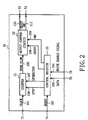
- FIG. 2 is a diagram showing the structure of the WDT 10.
- the WDT 10 comprises a counter 11, an output control circuit 12 and a control register 13.
- the WDT 10 has a plurality of terminals T1 to T6, and is connected to the CPU 1 and the oscillation circuit 3.
- the counter 11 is connected to the oscillation circuit 3 via the terminal T1, and receives a clock 101 supplied from the oscillation circuit 3.
- the counter 11 counts pulses (clock pulses) of the clock 101, in accordance with a stop control signal 106 and operation control signal 107 supplied from the control register 13.
- the counter 11 clears the counted value and counts the pulses of the clock 101. In the case where the counted value exceeds the limit value, the counter 11 outputs an over-flow signal 105 representing that the counted value has exceeded the limit value to the output control circuit 12. In response to the stop control signal 106, the counter 11 stops counting the pulses of the clock 101.
- the output control circuit 12 is connected to the CPU 1 via the terminals T2 and T3. In response to the over-flow signal 105 output from the counter 11, the output control circuit 12 outputs a reset signal 110 or NMI signal 111 to the CPU 1.
- the determination as to whether the reset signal 110 or the NMI signal 111 is output is made in accordance with a reset enable signal 108 and NMI enable signal 109 output from the control register 13 to the output control circuit 12. For example, in the case where the reset enable signal 108 is at a low level and the NMI enable signal 109 is at a high level, the reset signal 110 is output from the output control circuit 12. On the contrary, in the case where the reset enable signal 108 is at a high level and the NMI enable signal 109 is at a low level, the NMI signal 111 is output from the output control circuit 12.
- the CPU 1 In response to the reset signal 110 output from the output control circuit 12, the CPU 1 carries out the same initial process as that performed at the time the power source is applied thereto. In response to the NMI signal 111 sent from the output control circuit 12, the CPU 1 carries out a predetermined NMI process. Having performed the above, the microcomputer is restored to its normal state.
- the control register 13 is connected to the CPU 1 via the terminals T4, T5 and T6, and receives a reset signal 102, data 103 and a write enable signal 104 provided from the CPU 1.
- the control register 13 is initialized upon reception of the reset signal 102 from the CPU 1. Specifically, in response to the reset signal 102 from the CPU 1, the control register 13 outputs the operation control signal 107 to the counter 11, and sets the WDT 10 into a reset mode.
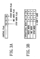
- the control register 13 has a control flag shown in FIG. 3A, and sets each of flags (bit value) included in the control flag, in accordance with the data 103 and write enable signal 104.
- the control register 13 sets the WDT 10 into an operational mode, in accordance with the control flag.
- FIG. 3B is a diagram showing the relationship between the flags included in the control flag and the operational modes of the WDT 10.
- the operational modes of the WDT 10 are represented by three bits B0, B1 and B2.
- the control register 13 In the case where the bit B0 is "0", the control register 13 outputs the operation control signal 107 to the counter 11 and sets the levels of the respective reset enable signal 108 and NMI enable signal 109, such that the output control circuit 12 outputs the reset signal 110. As a result of this, the WDT 10 is set into the reset mode. In this case, the counter 11 counts the pulses of the clock 101. Further, the output control circuit 12 outputs the reset signal 110, in the case where the counted value exceeds the limit value.
- the control register 13 outputs the operation control signal 107 to the counter 11 and sets the levels of the reset enable signal 10& and NMI enable signal 109, such that the output control circuit 12 outputs the NMI signal 111.
- the WDT 10 is set into the NMI mode.
- the counter 11 counts the pulses of the clock 101.
- the output control circuit 12 outputs the NMI signal 111, in the case where the counted value exceeds the limit value.
- control register 13 In the case where the bit B0 and bit B1 are both "1" and the bit B2 is "0", the control register 13 outputs the stop control signal 106 to the counter 11. Then, the WDT 10 is set into the stop mode. In this case, the counter 11 stops to operate.
- the reset signal 102 can be supplied to the control register 13 from circuits other than the CPU 1.
- the reset signal 110 output from the output control circuit 12 is supplied to the control register 13 as a reset signal 102.
- This reset signal 102 can be supplied also from a reset-signal output circuit (not illustrated) included in a device having the microcomputer. In response to user-pressing of a reset button set in the main body of the device, the reset-signal output circuit outputs the reset signal 102 to the CPU 1 and the control register 13.
- the CPU 1 In response also to the reset signal 102 sent from the reset-signal output circuit, the CPU 1 carries out the same initial process as that performed just when the power source is applied thereto.
- the control register 13 can be initialized in response to the reset signals 102 sent from the output control circuit 12 and reset-signal output circuit.
- the initial process which is carried out in response to the reset signal 110 output by the output control circuit 12 will hereinafter referred to as internal resetting, while the initial process which is carried out in response to the reset signal 102 output by the reset-signal output circuit will referred to as external resetting.
- a user of the device including the microcomputer presses a "reset" button set in the main body of the device.
- the reset signal 102 is supplied from the reset-signal output circuit to the CPU 1 and the control register 13.
- the CPU 1 carries out the external resetting in response to the reset signal 102 from the reset-signal output circuit, while the control register 13 is initialized in response to the reset signal 102 (Step S1).
- the CPU 1 reactivates the software program stored in the memory 2, in the external resetting (the initial process).
- the initialized control register 13 outputs the operation control signal 107 to the counter 11, and sets the WDT 10 into the reset mode.
- the counter 11 clears the counted value and counts the pulses of the clock 101 provided from the oscillation circuit 3 (Step S2).
- the CPU 1 outputs the reset signal 102 for clearing the counted value to the control register 13, in accordance with commends of the activated software program.
- the CPU 1 outputs the data 103 and write enable signal 104 for setting the operational mode of the WDT 10 to the control register 13, in accordance with the setting of the activated software program.
- Step S3 the CPU 1 carries out the above procedures. Hence, the counted value does not exceed the limit value (Step S3; NO).
- Step S3 In the case where an abnormal operation occurs in the microcomputer during the activation of the software program, the CPU 1 does not carry out the above procedures. Hence, the counted value exceeds the limit value (Step S3; YES).
- the counter 11 In the case where the counted value exceeds the limit value, the counter 11 outputs the over-flow signal 105 to the output control circuit 12. In response to the over-flow signal 105, the output control circuit 12 outputs the reset signal 110 to the CPU 1 and the control register 13.
- the CPU 1 In response to the reset signal 110 from the output control circuit 12, the CPU 1 carries out the internal resetting.
- the control register 13 is initialized in response to the reset signal 110 (the reset signal 102) (Step S4). Upon this, the above-described procedure of the step S2 is executed.
- the CPU 1 reactivates the software program stored in the memory 2.
- the initialized control register 13 outputs the operation control signal 107 to the counter 11 to set the WDT 10 into the reset mode, as described above.
- the CPU 1 In the case where the microcomputer normally operates, the CPU 1 outputs, as described above, the reset signal 102, the data 103 and the write enable signal 104, to the control register 13.
- the control register 13 sets the operational mode of the WDT 10, in accordance with the reset signal 102, the data 103 and the write enable signal 104 (Step S5).
- Step S5 the operational mode of the WDT 10 is the stop mode
- the counter 11 stops counting the pulses of the clock 101, in response to the stop control signal 106 supplied from the control register 13 (Step S6).
- the counter 11 clears the counted value in response to the operation control signal 107 supplied from the control register 13, and counts the pulses of the clock 101 supplied from the oscillation circuit 3 (Step S7).
- the CPU 1 outputs the reset signal 102 for clearing the counted value to the control register 13, in accordance with the commands of the software program.
- the control register 13 is initialized in response to the reset signal 102.
- the CPU 1 outputs the data 103 and the write enable signal 104 for maintaining the operational mode of the WDT 10 together with the reset signal 102, to the control register 13.
- Step S8; NO While the microcomputer normally operates, the CPU 1 repeats the above procedures, so that the counted value does not exceed the limit value
- the counter 11 In the case where the counted value exceeds the limit value, the counter 11 outputs the over-flow signal 105 to the output control circuit 12. In response to the over-flow signal 105, the output control circuit 12 outputs the reset signal 110 to the CPU 1 and control register 13. As a result of this, the above-described procedure of the step S4 is executed.
- control register 13 outputs the operation control signal 107 to the counter, in response to the reset signal 102 supplied from the CPU 1. Then, the counter 11 clears the counted value (Step S9), and the flow returns to the procedure of the step S7.
- the counter 11 clears the counted value, in response to the operation control signal 107 supplied from the control register 13, and counts the pulses of the clock 101 supplied from the oscillation circuit 3 (Step S10).
- the CPU 1 outputs the reset signal 102 for clearing the counted value, and the data 103 and write enable signal 104 for maintaining the operational mode of the WDT 10 to the control register 13, in accordance with the software program.
- Step S11; NO While the microcomputer normally operates, the CPU 1 repeats the above procedures, so that the counted value does not exceed the limit value
- Step S11 In the case where there is an abnormal operation occurring in the microcomputer, the CPU 1 does not execute the above procedures. Hence, the counted value exceeds the limit value (Step S11; YES).
- the counter 11 In the case where the counted value exceeds the limit value, the counter 11 outputs the over-flow signal 105 to the output control circuit 12, likewise the above. In response to the over-flow signal 105, the output control circuit 12 outputs the NMI signal 111 to the CPU 1. Upon this, the CPU 1 carries out a predetermined NMI process (Step S12).
- control register 13 outputs the operation control signal 107 to the counter 11, in response to the reset signal 102 supplied from the CPU 1. Upon this, the counter 11 clears the counted value (Step S13), and the flow returns to the procedure of the step S10.
- the WDT 10 operates in response to, not only the reset signal 102 output by the CPU 1, but the reset signals 102 and 110 for resetting the microcomputer (the CPU 1).
- the WDT 10 begins operating in synchronization with that the microcomputer (the CPU 1) begins the initial process (reset process).
- the WDT 10 can set the operations of the microcomputer back into a normal state, even if there is an abnormal operation occurring in the microcomputer during the activation of the software program.
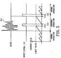
- a noise N11 in a power source causes an abnormal operation of the microcomputer,
- the CPU 1 does not output the reset signal 102, so the counted value reaches the limit value (C12).
- the output control circuit 12 outputs the reset signal 110 to the CPU 1 and the control register 13, as described above. Upon this, the CPU 1 begins the internal resetting, and the counter 11 clears the counted value (C13) and continues counting the pulses of the clock 101.
- the internal resetting begins, and the counted value is cleared (C15). At this time, if the noise N11 is removed therefrom, the microcomputer normally operates, and hence completing the internal resetting. In addition, the counted value is cleared before reaching the limit value.
- the WDT 10 functions immediately after the beginning of the internal resetting (or the external resetting). Hence, the WDT 10 can detect the abnormal operation which occurs in the microcomputer immediately after the beginning of the internal resetting (or the external resetting). As a result, operations of the microcomputer can be set back into the normal state.
- error data 103 and error write enable signal 104 may be provided from the CPU 1 to the control register 13.
- the operational mode of the WDT 10 is set in accordance with the data 103 and write enable signal 104. Hence, in the case where the abnormal operation occurs in the microcomputer, the operational mode of the WDT 10 may unintentionally be switched into another operational mode.
- the microcomputer can not get back into a normal operation state.
- control register 13 may include a circuit for setting the write enable signal 104 inactive after having set the operational mode of the WDT 10.
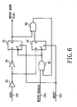
- the flag setting circuit comprises, as shown in FIG. 6, the first flop-flop (F/F) 21, the second F/F 22, the first inverter 23, the second inverter 24, the first AND gate 25 and the second AND gate 26.
- the reset signal 102 is input to reset terminals of the respective first and second F/F 21 and 22.
- the data 103 is reversed by the first inverter 23, further reversed by the second inverter 24, and then input to a data input-terminal of the first F/F 21.
- the data 103 having being reversed by the first inverter 23 is input to a data input-terminal of the. second F/F 22.
- the write enable signal 104 is input to the first AND gate 25.
- the first AND gate 25 outputs a logical product of the write enable signal 104 and a reverse signal of the signal output from the second AND gate 26, to clock terminals of the respective first F/F 21 and second F/F 22. Note, in this case, that the clock terminal of the first F/F 21 receives the signal which has been reversed and output from the first AND gate 25, and that the clock terminal of the first F/F 22 receives the signal as is from the first AND gate 25.
- the output signals of the first F/F 21 and 22 are input to the second AND gate 26.
- the output signal of the first F/F 21 is reversed and then input to the second AND gate 26, whereas the output signal of the second F/F 22 is input to the second AND gate 26 as is.
- the reset-mode flag (the value of the bit B0) is set based on the output signal of the first F/F 21.
- the first F/F 21 and second F/F 22 are reset in accordance with the reset signal 102. If the first F/F 21 and second F/F 2 are reset, the outputs of the first F/F 21. and second F/F 22 will be "0". In this case, the output of the second AND gate 26 is "0", and the write enable signal 104 is effective.
- the level of the signal output from the first F/F 21 is set to the level of the data 103, in synchronization with the input timing of this rising edge.
- the output of the F/F 21 is set to "0". In this case, the output of the second F/F 22 will be "1", and the output of the second AND gate 26 will be "1". Then, the write enable signal 104 will be ineffective.
- control register 13 includes the above-described circuit which sets the write enable signal 104 ineffective after setting the operational mode of the WDT 10, i.e. setting the control flag, it can be preventable that the operational mode of the WDT 10 is switched to another mode as a result of an abnormal operation of the microcomputer.
- the WDT according to the second embodiment is incorporated into a microcomputer, and has a plurality of operational modes.
- the microcomputer comprises the CPU 1, the memory 2, the oscillation circuit 3 and a WDT 30 according to the second embodiment.
- the WDT 30 comprises a counter 31, an output control circuit 32, a control register 33, a comparison register 34, a comparison circuit 35, a holding circuit 36 and an AND gate 37.
- the WDT 30 has terminals T7 to T12, and is connected to the CPU 1 and oscillation circuit 3.
- the counter 31, the output control circuit 32 and the control register 33 are substantially the same as the counter 11, the output control circuit 12 and the control register 13 included in the WDT 10 of the first embodiment. Note, however, that the counter 31 outputs the counted value to the comparison circuit 35.
- the comparison register 34 stores a threshold value which is smaller than a predetermined limit value, and outputs a signal representing the threshold value to the comparison circuit 35.
- the comparison circuit 35 compares the counted value sent from the counter 31 and the threshold value sent from the comparison register 34.
- the comparison circuit 35 outputs a result of the comparison to the holding circuit 36. Specifically, the comparison circuit 35 outputs "0" in the case where the counted value is smaller than the threshold value, and outputs "1" in the case where the counted value is equal to or larger than the threshold value.
- the holding circuit 36 holds the output of the comparison circuit 35, and outputs the held output to the AND gate 37. At this time, the output of the holding circuit 35 is reversed and then input to the AND gate 37.
- the AND gate 37 outputs a logical product of the write enable signal 104 provided from the CPU 1 and a reverse signal of the signal provided from the holding circuit 36, to the control register 33.
- the write enable signal 104 provided from the CPU 1 will be ineffective.
- the write enable signal 104 will not be provided to the control register 33.
- Steps S21 to S24 Those procedures (Steps S21 to S24) to be executed during the activation of the software program stored in the memory 2 are substantially the same as those explained in the first embodiment. Note, however, that if the predetermined allowable period elapses, the write enable signal 104 provided from the CPU 1 will be ineffective, as explained above.
- the CPU 1 sets the operational mode of the WDT 30 in accordance with the setting of the activated software program.
- the write enable signal 104 After the elapse of the predetermined allowable period, the write enable signal 104 is being ineffective. Thus, the CPU 1 outputs the reset signal 102 to the control register 33 to set the write enable signal 104 effective, and hence clearing the counted value (Step S25).
- the comparison circuit 35 If the counted value is cleared, i.e. the counted value is smaller than the threshold value, the comparison circuit 35 outputs "0" to the holding circuit 36. As a result of this, the write enable signal 104 will be effective.
- the CPU 1 outputs the data 103 and write enable signal 104 for setting the operational mode of the WDT 30 to the control register 33, in accordance with the activated software program.
- the control register 33 sets the operational mode of the WDT 30, in accordance with the data 103 and write enable signal 104, likewise the case of the first embodiment (Step S26).
- Steps S27 to S34 Those procedures (Steps S27 to S34) after the operational mode of the WDT 30 is set are substantially the same as those of the first embodiment. Note, however, that if the predetermined allowable period elapses, the write enable signal 104 provided from the CPU 1 will be ineffective, as described above.
- the operational mode of the WDT 30 is switched to another mode as a result of an abnormal operation of the microcomputer, by setting a period of time the write enable signal 104 is effective, i.e. by setting a period of 'time the operational mode of the WDT 30 can be set.
- the WDT 30 can operate in accordance with not only the reset signal 102 output by the CPU 1, but also the reset signals 102 and 110 for resetting the microcomputer (the CPU 1). Thus, even if an abnormal operation occurs in the microcomputer during the activation of the software program, the WDT 30 can set the operations of the microcomputer back into a normal state.
- the control register 33 included in the WDT 30 may include a flag setting circuit described in the first embodiment.
- the apparatus of the present invention can be realized by a general computer, without the need for a dedicated system.
- a program and data for controlling a computer to execute the above-described procedures may be recorded on a medium (a floppy disk, CD-ROM, DVD or the like) and distributed, and the program may be installed into the computer and run on an OS (Operating System) to execute the above-described processes, thereby achieving the apparatus of the present invention.
- the above program and data may be stored in a disk device or the like in the server device on the Internet, and embedded in a carrier wave.
- the program and data embedded in the carrier wave may be downloaded into the computer so as to realize the apparatus of the present invention.
Landscapes
- Engineering & Computer Science (AREA)
- Theoretical Computer Science (AREA)
- Quality & Reliability (AREA)
- Physics & Mathematics (AREA)
- General Engineering & Computer Science (AREA)
- General Physics & Mathematics (AREA)
- Debugging And Monitoring (AREA)
- Microcomputers (AREA)
Abstract
Description
the timer (10,30) may set an operational mode thereof, in accordance with the mode specification signal (103, 104).
Claims (18)
- A computer characterized by comprising:characterized in that said controller (1) controls said timer (10, 30), and clears the counted value before the counted value exceeds the limit value, anda controller (1) which executes a reset process, in response to a reset signal (102, 110);an oscillator (3) oscillates a clock (101); anda timer (10, 30) which counts pulses of the clock (101), and outputs the reset signal (110) to said controller, in a case where a counted value obtained by counting the pulses of the clock (101) exceeds a predetermined limit value; and
said timer (10, 30) begins counting the pulses of the clock (101) in synchronization with that said controller (1) begins the reset process, thereby detecting an abnormal operation occurring in the computer during execution of the reset process. - The computer according to claim 1, characterized in that
said timer (10, 30) has a plurality of operational modes. - The computer according to claim 2, characterized in that:said controller (1) outputs a mode specification signal (103, 104) for specifying an operational mode of said timer (10, 30), to said timer (10, 30); andsaid timer (10, 30) sets an operational mode thereof, in accordance with the mode specification signal (103, 104).
- The computer according to claim 3, characterized in that
said timer (10, 30) includes a circuit, which sets the mode specification signal (104) sent from said controller (1) ineffective in response to setting of the operational mode of said timer (10, 30). - The computer according to claim 3, characterized in that
said timer (30) further includes a restriction circuit (34, 35, 36, 37) which restricts an allowable period of time the mode specification signal (104) provided from said controller (1) can be accepted. - The computer according to claim 4, characterized in that
said timer (30) further includes a restriction circuit (34, 35, 36, 37) which restricts an allowable period of time the mode specification signal (104) provided from said controller (1) can be accepted. - A watchdog timer characterized by comprising:characterized in that said counter (11, 13, 31, 33) clears the counted value and begins counting the pulses of the clock (101) in response to the reset signal (110) output from said output circuit (12, 32), thereby detecting an abnormal operation occurring in said external circuit (1) during execution of the reset process.a counter (11, 13, 31, 33) which counts pulses of a clock (101) generated by an oscillator (3), and clears a counted value of the pulses, in response to a clear signal (102) for designating to clear the counted value and being supplied from an external circuit (1); andan output circuit (12, 32) which outputs a reset signal (110) for designating to execute a reset process to said external circuit (1), in a case where the counted value exceeds a predetermined limit value, and
- The watchdog timer according to claim 7, characterized in that
said watchdog timer has a plurality of operational modes. - The watchdog timer according to claim 8, characterized by further includinga mode setting circuit (13, 33) which sets an operational mode of said watchdog timer, in accordance with a mode specification signal (103, 104) which specifies the operational mode and is provided from said external circuit (1).
- The watchdog timer according to claim 9, characterized by further includinga circuit which sets the mode specification signal (104) sent from said external circuit (1) ineffective, in response to setting of the operational mode of said watchdog timer.
- The watchdog timer according to claim 9, characterized by further includinga restriction circuit (34, 35, 36, 37) which restricts an allowable period of time the mode specification signal (104) provided from said external circuit (1) can be accepted.
- The watchdog timer according to claim 10, characterized by further includinga restriction circuit (34, 35, 36, 37) which restricts an allowable period of time the mode specification signal (104) provided from said external circuit (1) can be accepted.
- An abnormal operation detection method characterized by comprising:characterized in that said counting includes detecting an abnormal operation occurring in said external circuit (1) during execution of the reset process, by counting the pulses of the clock (101) in synchronization with that said external circuit begins the reset process.counting pulses of a clock (101) generated by an oscillator (3);clearing a counted value of the pulses, in response to a clear signal (102) which is provided from an external circuit (1) and designates to clear the counted value; andcontrolling said external circuit (1) to execute a reset process, in a case where the counted value exceeds a predetermined limit value, and
- The detection method according to claim 13, characterized in that
said detection methods includes a plurality of modes. - The detection method according to claim 14, characterized by further includingsetting a mode of the detection method, in accordance with a mode specification signal (103, 104) which is provided from said external circuit (1) and specifies the mode.
- The detection method according to claim 15, characterized by further includingsetting the mode specification signal (104) which is provided from said external circuit (1) ineffective, in response to setting of the mode.
- The detection method according to claim 15, characterized by further includingrestricting an allowable period of time the mode specification signal (104) provided from said external circuit (1) can be accepted.
- The detection method according to claim 16, characterized by further includingrestricting an allowable period of time the mode specification signal (104) provided from said external circuit (1) can be accepted.
Applications Claiming Priority (2)
| Application Number | Priority Date | Filing Date | Title |
|---|---|---|---|
| JP2000390716 | 2000-12-22 | ||
| JP2000390716A JP2002189614A (en) | 2000-12-22 | 2000-12-22 | Watchdog timer, microcomputer with the same built therein, and control method for preventing runaway of microcomputer |
Publications (2)
| Publication Number | Publication Date |
|---|---|
| EP1217522A2 true EP1217522A2 (en) | 2002-06-26 |
| EP1217522A3 EP1217522A3 (en) | 2003-04-02 |
Family
ID=18857027
Family Applications (1)
| Application Number | Title | Priority Date | Filing Date |
|---|---|---|---|
| EP01130680A Withdrawn EP1217522A3 (en) | 2000-12-22 | 2001-12-21 | Watchdog timer and method for detecting abnormal operation of computer, and computer including the timer |
Country Status (4)
| Country | Link |
|---|---|
| US (1) | US6948103B2 (en) |
| EP (1) | EP1217522A3 (en) |
| JP (1) | JP2002189614A (en) |
| KR (1) | KR20020051882A (en) |
Cited By (4)
| Publication number | Priority date | Publication date | Assignee | Title |
|---|---|---|---|---|
| WO2005119739A3 (en) * | 2004-06-04 | 2006-04-13 | Conti Temic Microelectronic | Electronic component for preventing undesired switching between monitoring modes |
| CN101895440A (en) * | 2010-07-22 | 2010-11-24 | 北京天融信科技有限公司 | Security gateway and failure detection method thereof |
| CN101685651B (en) * | 2008-09-24 | 2013-02-13 | 上海国宽信息科技有限公司 | Watchdog reset circuit for vehicle-mounted displayer |
| CN113342572A (en) * | 2021-06-08 | 2021-09-03 | 深圳市航顺芯片技术研发有限公司 | Automatic watchdog overloading system, method, equipment and storage medium |
Families Citing this family (14)
| Publication number | Priority date | Publication date | Assignee | Title |
|---|---|---|---|---|
| JP3636031B2 (en) * | 2000-04-28 | 2005-04-06 | 株式会社デンソー | Microcomputer monitoring method in electronic control unit |
| US6892332B1 (en) * | 2001-11-01 | 2005-05-10 | Advanced Micro Devices, Inc. | Hardware interlock mechanism using a watchdog timer |
| JP2003150408A (en) * | 2001-11-15 | 2003-05-23 | Sumitomo Denko Brake Systems Kk | Monitoring method for microcomputer for on-vehicle controller and circuit thereof |
| DE10203807C1 (en) * | 2002-01-31 | 2003-07-31 | Siemens Ag | Method and circuit arrangement for monitoring the function of a processor |
| US7689875B2 (en) * | 2002-04-25 | 2010-03-30 | Microsoft Corporation | Watchdog timer using a high precision event timer |
| US20040250178A1 (en) * | 2003-05-23 | 2004-12-09 | Munguia Peter R. | Secure watchdog timer |
| JP2007228765A (en) * | 2006-02-24 | 2007-09-06 | Fuji Electric Fa Components & Systems Co Ltd | Inverter device with time counting function |
| KR100824792B1 (en) * | 2006-07-11 | 2008-04-24 | 삼성전자주식회사 | Command processing device and method and system comprising same |
| US20080016385A1 (en) * | 2006-07-13 | 2008-01-17 | Hollingsworth Robert E | Plain Language Announcement of Diagnostic and Troubleshooting Information for Users |
| KR101172387B1 (en) | 2006-09-12 | 2012-08-08 | 주식회사 만도 | Calculation Error Testing Device For Micro Control Unit Using Serial Peripheral Interface |
| US7783872B2 (en) * | 2007-03-30 | 2010-08-24 | Dell Products, Lp | System and method to enable an event timer in a multiple event timer operating environment |
| US8832505B2 (en) | 2012-06-29 | 2014-09-09 | Intel Corporation | Methods and apparatus to provide failure detection |
| CN103530197B (en) * | 2013-10-29 | 2017-06-13 | 浙江宇视科技有限公司 | A kind of method for detecting and solving Linux system deadlock |
| JP7304731B2 (en) * | 2019-04-16 | 2023-07-07 | ローム株式会社 | watchdog timer |
Family Cites Families (9)
| Publication number | Priority date | Publication date | Assignee | Title |
|---|---|---|---|---|
| DE3207120A1 (en) | 1982-02-27 | 1983-09-08 | Felten & Guilleaume Fernmeldeanlagen GmbH, 8500 Nürnberg | Monitoring circuit for a microcomputer |
| JPS6162947A (en) | 1984-09-04 | 1986-03-31 | Kubota Ltd | How to prevent a computer from running out of control |
| JPS61296443A (en) | 1985-06-24 | 1986-12-27 | Mitsubishi Electric Corp | Watchdog timer |
| JPS6341951A (en) | 1986-08-07 | 1988-02-23 | Sanyo Electric Co Ltd | Microcomputer |
| US4866713A (en) * | 1987-11-02 | 1989-09-12 | Motorola, Inc. | Operational function checking method and device for microprocessors |
| US5541943A (en) * | 1994-12-02 | 1996-07-30 | At&T Corp. | Watchdog timer lock-up prevention circuit |
| US5864663A (en) * | 1996-09-12 | 1999-01-26 | United Technologies Corporation | Selectively enabled watchdog timer circuit |
| US6260162B1 (en) * | 1998-10-31 | 2001-07-10 | Advanced Micro Devices, Inc. | Test mode programmable reset for a watchdog timer |
| US6560726B1 (en) * | 1999-08-19 | 2003-05-06 | Dell Usa, L.P. | Method and system for automated technical support for computers |
-
2000
- 2000-12-22 JP JP2000390716A patent/JP2002189614A/en active Pending
-
2001
- 2001-12-20 US US10/028,111 patent/US6948103B2/en not_active Expired - Fee Related
- 2001-12-21 KR KR1020010082818A patent/KR20020051882A/en not_active Ceased
- 2001-12-21 EP EP01130680A patent/EP1217522A3/en not_active Withdrawn
Cited By (6)
| Publication number | Priority date | Publication date | Assignee | Title |
|---|---|---|---|---|
| WO2005119739A3 (en) * | 2004-06-04 | 2006-04-13 | Conti Temic Microelectronic | Electronic component for preventing undesired switching between monitoring modes |
| CN101685651B (en) * | 2008-09-24 | 2013-02-13 | 上海国宽信息科技有限公司 | Watchdog reset circuit for vehicle-mounted displayer |
| CN101895440A (en) * | 2010-07-22 | 2010-11-24 | 北京天融信科技有限公司 | Security gateway and failure detection method thereof |
| CN101895440B (en) * | 2010-07-22 | 2012-07-04 | 北京天融信科技有限公司 | Security gateway and failure detection method thereof |
| CN113342572A (en) * | 2021-06-08 | 2021-09-03 | 深圳市航顺芯片技术研发有限公司 | Automatic watchdog overloading system, method, equipment and storage medium |
| CN113342572B (en) * | 2021-06-08 | 2022-11-29 | 深圳市航顺芯片技术研发有限公司 | Automatic watchdog overloading system, method, equipment and storage medium |
Also Published As
| Publication number | Publication date |
|---|---|
| US20020083375A1 (en) | 2002-06-27 |
| US6948103B2 (en) | 2005-09-20 |
| KR20020051882A (en) | 2002-06-29 |
| EP1217522A3 (en) | 2003-04-02 |
| JP2002189614A (en) | 2002-07-05 |
Similar Documents
| Publication | Publication Date | Title |
|---|---|---|
| EP1217522A2 (en) | Watchdog timer and method for detecting abnormal operation of computer, and computer including the timer | |
| US6038671A (en) | Power management of a computer system using a power button | |
| JPH0528063A (en) | Microcomputer | |
| CN101796489A (en) | Clock supervision unit | |
| JP2006171952A (en) | Semiconductor integrated circuit device | |
| US6463492B1 (en) | Technique to automatically notify an operating system level application of a system management event | |
| US6321289B1 (en) | Apparatus for automatically notifying operating system level applications of the occurrence of system management events | |
| JP2007534049A (en) | Watchdog system and method for monitoring processor functionality | |
| JP5241450B2 (en) | Semiconductor device and abnormality detection method thereof | |
| WO2004003714A2 (en) | Circuit for detection of internal microprocessor watchdog device execution and method for resetting microprocessor system | |
| US12093118B2 (en) | Watchdog timer device | |
| CN119597129B (en) | Reset circuit | |
| JP3088395B2 (en) | Switch interrupt processing circuit and switch interrupt processing method | |
| JP2000035903A (en) | Runaway monitoring device for microcomputer | |
| JP2003044324A (en) | Method, device and program for confirming abnormality detection | |
| JP3406418B2 (en) | Power failure interrupt signal detection circuit | |
| US7080281B2 (en) | Method and circuit arrangement for monitoring the operation of a processor | |
| TWM626658U (en) | Computer system | |
| TW202530980A (en) | Computer system control method, control device, computer system, computer equipment and computer readable storage medium | |
| JP3219438B2 (en) | I/O control unit status storage method | |
| CN118259717A (en) | Switching control method, system, chip, electronic device and storage medium of system clock | |
| JPH0744399A (en) | Interruption control circuit | |
| JPH11327959A (en) | Method and device for monitoring abnormality of processor | |
| JPH03204739A (en) | Microcomputer | |
| JPH03105514A (en) | Power-off detection/recovery circuit |
Legal Events
| Date | Code | Title | Description |
|---|---|---|---|
| PUAI | Public reference made under article 153(3) epc to a published international application that has entered the european phase |
Free format text: ORIGINAL CODE: 0009012 |
|
| AK | Designated contracting states |
Kind code of ref document: A2 Designated state(s): AT BE CH CY DE DK ES FI FR GB GR IE IT LI LU MC NL PT SE TR |
|
| AX | Request for extension of the european patent |
Free format text: AL;LT;LV;MK;RO;SI |
|
| PUAL | Search report despatched |
Free format text: ORIGINAL CODE: 0009013 |
|
| AK | Designated contracting states |
Kind code of ref document: A3 Designated state(s): AT BE CH CY DE DK ES FI FR GB GR IE IT LI LU MC NL PT SE TR Designated state(s): AT BE CH CY DE DK ES FI FR GB GR IE IT LI LU MC NL PT SE TR |
|
| AX | Request for extension of the european patent |
Extension state: AL LT LV MK RO SI |
|
| 17P | Request for examination filed |
Effective date: 20030218 |
|
| RAP1 | Party data changed (applicant data changed or rights of an application transferred) |
Owner name: NEC ELECTRONICS CORPORATION |
|
| 17Q | First examination report despatched |
Effective date: 20030530 |
|
| AKX | Designation fees paid |
Designated state(s): DE FR IT |
|
| STAA | Information on the status of an ep patent application or granted ep patent |
Free format text: STATUS: THE APPLICATION HAS BEEN WITHDRAWN |
|
| 18W | Application withdrawn |
Effective date: 20040413 |