EP1209810B1 - Pulse width modulator responsive to external signals - Google Patents
Pulse width modulator responsive to external signals Download PDFInfo
- Publication number
- EP1209810B1 EP1209810B1 EP01309477A EP01309477A EP1209810B1 EP 1209810 B1 EP1209810 B1 EP 1209810B1 EP 01309477 A EP01309477 A EP 01309477A EP 01309477 A EP01309477 A EP 01309477A EP 1209810 B1 EP1209810 B1 EP 1209810B1
- Authority
- EP
- European Patent Office
- Prior art keywords
- register
- data
- signal
- cpu
- bus
- Prior art date
- Legal status (The legal status is an assumption and is not a legal conclusion. Google has not performed a legal analysis and makes no representation as to the accuracy of the status listed.)
- Expired - Lifetime
Links
- 230000004044 response Effects 0.000 claims description 23
- 101100446506 Mus musculus Fgf3 gene Proteins 0.000 claims description 10
- 230000007274 generation of a signal involved in cell-cell signaling Effects 0.000 claims description 2
- 238000010586 diagram Methods 0.000 description 8
- 230000000630 rising effect Effects 0.000 description 6
- 101000767160 Saccharomyces cerevisiae (strain ATCC 204508 / S288c) Intracellular protein transport protein USO1 Proteins 0.000 description 4
- 238000003708 edge detection Methods 0.000 description 3
- 238000000034 method Methods 0.000 description 2
- 230000003111 delayed effect Effects 0.000 description 1
- 230000004048 modification Effects 0.000 description 1
- 238000012986 modification Methods 0.000 description 1
- 230000000737 periodic effect Effects 0.000 description 1
Images


Classifications
-
- G—PHYSICS
- G06—COMPUTING; CALCULATING OR COUNTING
- G06F—ELECTRIC DIGITAL DATA PROCESSING
- G06F1/00—Details not covered by groups G06F3/00 - G06F13/00 and G06F21/00
- G06F1/02—Digital function generators
- G06F1/025—Digital function generators for functions having two-valued amplitude, e.g. Walsh functions
-
- H—ELECTRICITY
- H03—ELECTRONIC CIRCUITRY
- H03K—PULSE TECHNIQUE
- H03K7/00—Modulating pulses with a continuously-variable modulating signal
- H03K7/08—Duration or width modulation ; Duty cycle modulation
Definitions
- the present invention generally relates to PWM (pulse width modulation) apparatuses that output a pulse signal based on pulse width modulation, and particularly relates to a PWM apparatus that modifies a pulse waveform at a predetermined timing.
- PWM pulse width modulation
- a PWM (pulse width modulation) apparatus outputs a pulse signal having a specified cycle and a specified duty ratio.
- the pulse signal output from the PWM apparatus may be used to control motor revolution for the purpose of attending to auto-focus control of a camera apparatus or the like.
- a CPU accesses the PWM apparatus to change the cycle and duty ratio, thereby controlling the waveform of the output pulse signal.
- EP-A-0657988 discloses such a devices, corresponding to the preamble portion of Claim 1.
- the timer When there is a need to modify the waveform of a pulse signal in response to an external event such as a trigger from a timer, the timer generates an interruption to the CPU.
- the CPU executes an interruption routine, and updates data of the PWM waveform stored in the PWM apparatus by using a bus as an access route.
- the waveform of a pulse signal output from the PWM apparatus changes accordingly.
- a device for generating a pulse signal comprising: at least one first register which stores waveform data therein; and a pulse signal generation unit which generates a pulse signal in accordance with the waveform data of said first register; characterized by: a control unit which is connected to a bus, and is controlled by control signals supplied from the bus, and a signal line which is separate from and independent of the bus, and is connected to said control unit, wherein said control unit fetches update data for the said first register from said bus based on the said control signal and updates the waveform data of said first register with the update data in response to a signal that is externally supplied through said signal line, said update data including data indicative of a period of the pulse signal and data indicative of a duty ratio of the pulse signal.
- the external signal is supplied to the control unit through the signal line that is directly connected to the control unit independently from the bus.
- the control unit updates the waveform data such as duty data and cycle data stored in the registers, thereby effecting a change in the PWM waveform of the output pulse signal. In this manner, it is possible to modify the PWM waveform at a desired timing indicated by an external event.
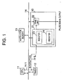
- Fig.1 is a block diagram of a PWM system according to the present invention.
- the system of Fig.1 includes a PWM apparatus 10, a CPU 11, a timer 12, an instruction memory 13, and a CPU bus 14.
- the PWM apparatus 10, the CPU 11, the timer 12, and the instruction memory 13 are connected together via the CPU bus 14.
- the CPU 11 operates based on programs that are a series of instructions stored in the instruction memory 13.
- the timer 12 is controlled by the CPU 11, for example, via the CPU bus 14, and marks time by counting clock pulses or the like.
- the timer 12 When detecting an arrival of a preset time such as at an end of a predetermined time interval, the timer 12 generates an interruption signal.
- the interruption signal is supplied to the CPU 11 via an interruption signal line int1 and to the PWM apparatus 10 via an interruption signal line int2.
- the PWM apparatus 10 is connected to the CPU bus 14, and is controlled by the CPU 11. Further, the PWM apparatus 10 receives the interruption signal from the timer 12 via the interruption signal line int2.
- the PWM apparatus 10 includes a PWM unit 22 and a control unit 21 where the PWM unit 22 has substantially the same configuration as a conventional PWM unit, and the control unit 21 includes registers 23 and 24.
- the control unit 21 receives the interruption signal from the timer 12 via the interruption signal line int2, and, in response, supplies a duty setting and a cycle setting stored in the respective registers 23 and 24 to the PWM unit 22.
- the PWM unit 22 stores the received duty setting and cycle setting in internal registers, and outputs a pulse signal in accordance with the renewed settings. With this, the output pulse signal is changed from an old PWM waveform to a new PWM waveform.
- the CPU 11 Upon receiving an interruption signal from the timer 12 through the interruption signal line int1, the CPU 11 obtains a duty ratio and a cycle for a next PWM waveform, for example, based on computation or data stored in a memory.
- the CPU 11 supplies the duty ratio and the cycle to the PWM apparatus 10 through the CPU bus 14.
- the transferred duty ratio and cycle are stored in the respective registers 23 and 24 of the control unit 21 as a duty ratio and a cycle for a next PWM waveform, for example.
- the duty ratio and cycle that are stored in the respective registers 23 and 24 in response to the interruption from the timer 12 to the CPU 11 are provided as preparation for an immediately following interruption, for example.
- the registers 23 and 24 may be implemented by using FIFOs or sets of registers.
- the CPU 11 responds to the interruption sent from the timer 12 via the interruption signal line int1 by supplying a duty ratio and a cycle that are to be used for a second next interruption, a third next interruption, etc., in stead of a next and immediately following interruption.
- the registers 23 and 24 may not be registers each for storing a single piece of data therein, but may serve as register queues for storing a series of data pieces such as next data, second next data, third next data, and so on.
- the CPU 11 can generate next data reliably prior to a next event of interruption and can supply the data to the PWM apparatus 10, there is not necessarily a need to await an interruption signal supplied from the timer 12 via the interruption signal line int1 before supplying data. Further, if register queues are employed, and if it is possible for the CPU 11 to compute data for future needs beforehand, the CPU 11 may compute data for next ten interruptions, for example, and may supply the data through the CPU bus 14 to the PWM apparatus 10, thereby storing the data for the next ten interruptions in the register queues at once.
- the interruption signal from the timer 12 is directly supplied to the PWM apparatus 10.
- the PWM apparatus 10 supplies settings such as the duty setting and the cycle setting stored in the registers to the PWM unit 22, which is used to actually generate a pulse signal. This achieves a change in the PWM waveform of the output pulse signal. In this manner, it is possible to modify the PWM waveform at a desired timing indicated by an external event such as a trigger from the timer 12.
- the settings such as the duty setting and the cycle setting stored in the registers of the PWM apparatus 10 are supplied from the CPU 11 to the PWM apparatus 10 via the CPU bus 14 in response to an interruption signal issued by the timer 12, for example.
- the settings of data may be made successively for the immediately following interruption, or may be made at once with respect to data for a plurality of future interruptions.
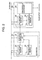
- Fig.2 is a block diagram of a first embodiment of the PWM apparatus 10 according to the present invention.
- the same elements as those of Fig.1 are referred to by the same numerals, and a description thereof will be omitted.
- the control unit 21 includes the duty setting register 23 and the cycle setting register 24. Further, the control unit 21 includes a selector-&-controller unit 31.
- the duty setting register 23 and the cycle setting register 24 are directly connected to the CPU bus 14, and receive duty data and cycle data, respectively, from the CPU 11 through the CPU bus 14.
- the CPU bus 14 includes an address bus, a data bus, and a control signal bus for conveying a chip selecting signal, a read/write signal, and the like.
- the selector-&-controller unit 31 receives control signals from the control signal bus, and controls data write/read operations in respect of the duty setting register 23 and the cycle setting register 24 in accordance with the received control signals. Further, the selector-&-controller unit 31 receives an interruption signal from the timer 12, and controls data transfer operations for transferring data from the duty setting register 23 and the cycle setting register 24 to the PWM unit 22 in accordance with the received interruption signal.
- the PWM unit 22 includes a duty setting register 32, a cycle setting register 33, and a PWM-control-&-counter unit 34.
- the duty setting register 32 and the cycle setting register 33 are directly connected to the CPU bus 14.
- the PWM-control-&-counter unit 34 operates as a unit that generates a pulse signal, and generates a pulse signal in accordance with the data stored in the duty setting register 32 and the cycle setting register 33, thereby outputting the pulse signal to the exterior of the device.
- the PWM unit 22 has substantially the same configuration as a conventional PWM apparatus, and is capable of modifying the PWM waveform of the pulse signal output under the control of the CPU in accordance with the data stored in the duty setting register 32 and the cycle setting register 33 in the same manner as in the conventional art.
- the PWM unit 22 is additionally configured such that the duty setting register 32 allows data thereof to be written by the selector-&-controller unit 31.
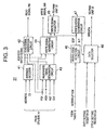
- Fig.3 is a block diagram showing a example configuration of the selector-&-controller unit 31.
- the selector-&-controller unit 31 includes an address decoder 41, a read-signal generation circuit 42, a read/write-timing generation circuit 43, a write-signal generation circuit 44, a write-signal selector 45, a rising-edge detection circuit 46, a write-state generation circuit 47, and a data selector 48.
- Fig.4 is a timing chart for explaining operations of the selector-&-controller unit 31 of Fig.3 when data is written in and read from the duty setting register 23 and the cycle setting register 24. In the following, data read/write operations with respect to the register queues will be described with reference to Fig.2, Fig.3, and Fig.4.
- control signals are supplied from the CPU 11 to the selector-&-controller unit 31 of the control unit 21 through the CPU bus 14.
- These control signals include a chip selecting signal CS, a read signal RDX, a write signal WRX, a reset signal RST, and a clock signal CLK.
- the chip selecting signal CS is supplied to the address decoder 41.
- the read signal RDX, the write signal WRX, the reset signal RST, and the clock signal CLK are supplied to the read/write-timing generation circuit 43.
- Address signals are conveyed through the address bus of the CPU bus 14 in synchronization with the chip selecting signal CS, and are supplied to the address decoder 41.
- (a) through (f) show timing relations between these signals.
- the address decoder 41 receives the address signals in addition to the chip selecting signal CS, and decodes the received address.
- the address decoder 41 generates an address match signal as shown in (f) of Fig.4 when the chip selecting signal CS selects this chip among other chips while the received address matches an address of the register of the PWM apparatus 10.
- the address match signal is supplied to the read-signal generation circuit 42 and the write-signal generation circuit 44.
- the read/write-timing generation circuit 43 Based on the clock signal CLK, the read/write-timing generation circuit 43 generates a read timing signal indicative of a timing of a read operation, and generates a write timing signal indicative of a timing of a write operation.
- the read timing signal is supplied to the read-signal generation circuit 42, and the write timing signal is supplied to the write-signal generation circuit 44.
- the read-signal generation circuit 42 generates a read signal RD (as shown in Fig.4, (i)) at a timing specified by the read timing signal when the read signal RDX indicates a read operation while the address match signal is activated.
- the write-signal generation circuit 44 generates a write signal WR (as shown in Fig.4, (j)) at a timing specified by the write timing signal when the write signal WRX indicates a write operation whilst the address match signal is activated.
- These read signal RD and write signal WR are supplied to the duty setting register 23 and the cycle setting register 24, thereby ordering a read operation and a write operation in respect of these registers.
- the read signal RD orders a read operation
- data is read from the register of an indicated address, and is output to the data bus of the CPU bus 14.
- the write signal WR orders a write operation
- data conveyed through the data bus of the CPU bus 14 is written in the register queue at an indicated address.
- the data signal of the data bus is shown in Fig.4, (g).
- the CPU 11 carries out a data write operation and a data read operation in respect of the duty setting register 23 and the cycle setting register 24 of the control unit 21.
- the CPU 11 may perform a data write operation and a data read operation with respect to the duty setting register 32 and the cycle setting register 33 of the PWM unit 22.
- Fig.5 is a timing chart for explaining operations performed by the selector-&-controller unit 31 when the timer 12 generates an interruption signal. Operations of modifying the waveform of a pulse signal will be described with reference to Fig.2, Fig.3, and Fig.5.
- the interruption signal generated by the timer 12 arrives at the selector-&-controller unit 31 of the control unit 21.
- the interruption signal arriving at the selector-&-controller unit 31 is supplied to the rising-edge detection circuit 46.
- the rising-edge detection circuit 46 detects a rising edge of the interruption signal to generate a rising edge pulse EGP.
- the rising edge pulse EGP is supplied to the write-signal selector 45 and the write-state generation circuit 47.
- the write-signal selector 45 In response to the rising edge pulse EGP, the write-signal selector 45 generates write signals PWMWR respectively for the cycle setting purpose and for the duty setting purpose, and these generated signals are supplied to the PWM unit 22.
- the write-state generation circuit 47 responsive to the rising edge pulse EGP, changes an internal state thereof, and generates a selection signal SLT accordingly.
- the selection signal SLT is supplied to the data selector 48.
- the interruption signal, the rising edge pulse EGP, the internal state of the write-state generation circuit 47, the write signal PWMWR for the cycle setting, the write signal PWMWR for the duty setting, and the selection signal SLT described above are shown in Fig.5, (a) through (f), respectively.
- the data selector 48 selects data of a register indicated by the selection signal SLT.
- the selection signal SLT is HIGH, for example, data of the cycle setting register 24 is selected.
- the selection signal is LOW, on the other hand, data of the duty setting register 23 is selected.
- the selection signal SLT is HIGH when the data of the cycle setting register 24 is to be selected, and is LOW when the data of the duty setting register 23 is to be selected.
- the write data WRDATA (Fig.5, (i)) supplied to the PWM unit 22 turns into data CYCLE#00 that is the first data of the cycle setting register 24.
- the write data WRDATA (Fig.5, (i)) supplied to the PWM unit 22 turns into data DUTY#00 that is the first data of the duty setting register 23.
- the data CYCLE#00 of the write data WRDATA that is the first data of the cycle setting register 24 is stored in the cycle setting register 33 in response to the write signal PWMWR for the cycle setting (Fig.5, (d)).
- the data DUTY#00 of the write data WRDATA that is the first data of the duty setting register 23 is stored in the duty setting register 32 in response to the write signal PWMWR for the duty setting (Fig.5, (e)).
- the configuration of Fig.2 is designed such that data for cycle setting is temporarily stored in the duty setting register 32 first, and, then, is transferred from the duty setting register 32 to the cycle setting register 33.
- the data of the cycle setting register 24 is updated to the second data (#01) after the first data (#00) is read therefrom.
- writing of data in the cycle setting register 24 is carried out in the manner as described with reference to the Fig.4.
- the data of the duty setting register 23 is updated to the second data (#01) after the first data (#00) is read therefrom. Writing of data in the duty setting register 23 in this regard is carried out in the manner as described with reference to the Fig.4.
- an interruption signal from the timer 12 is directly supplied to the PWM apparatus 10.
- the PWM apparatus 10 supplies settings such as the duty setting and the cycle setting stored in the registers to the PWM unit 22, which is used to actually generate a pulse signal. This achieves a change in the PWM waveform of the output pulse signal.
- the settings such as the duty setting and the cycle setting stored in the registers of the PWM apparatus 10 are supplied from the CPU 11 to the PWM apparatus 10 via the CPU bus 14 in response to an interruption signal issued by the timer 12, for example.
- the setting of data is made successively for the immediately following interruption.
- Fig. 6 is a block diagram of a second embodiment of the PWM apparatus 10 according to the present invention.
- the same elements as those of Fig.2 are referred to by the same numerals, and a description thereof will be omitted.
- setting of data by the CPU is directed to data for the next and immediately following interruption.
- the second embodiment is configured such that data for a plurality of future interruptions are stored at once or successively in advance.
- the second embodiment of Fig.6 has a duty setting register queue 23A and a cycle setting register queue 24A, which replace the duty setting register 23 and the cycle setting register 24, respectively.
- the duty setting register queue 23A and the cycle setting register queue 24A may each be comprised of a FIFO (first-in first-out) or the like from which data is successively read in the same order as the data is successively stored. In this case, not only data for the next interruption but also data for the second next interruption, data for the third next interruption, etc., may be computed while there is no other load on the CPU 11, for example, and are stored in the duty setting register queue 23A and the cycle setting register queue 24A at once or successively in advance.
- FIFO first-in first-out
- the duty setting register queue 23A and the cycle setting register queue 24A may each be comprised of a set of registers having respective addresses assigned thereto.
- data for the next interruption but also data for the second next interruption, data for the third next interruption, etc. may be computed while there is no other load on the CPU 11, for example, and are stored in the duty setting register queue 23A and the cycle setting register queue 24A at once or successively in advance.
- data can be written by indicating a writing address. Because of this, after writing data for ten future interruptions, the data for the sixth through tenth future interruptions can be changed, for example, by specifying respective addresses if data changes become necessary upon situational changes.
- data that is supplied from the duty setting register queue 23A and the cycle setting register queue 24A to the PWM unit 22 by the selector-&-controller unit 31 is the data that is successively output from the FIFOs.
- means to indicate an address of next data may be provided by a counter or the like, and data of the register indicated by this address indicating means may be supplied successively from the duty setting register queue 23A and the cycle setting register queue 24A to the PWM unit 22.
- an external event for triggering modification of the pulse signal waveform is an event of a timer.
- the external event is not limited to an even of a timer, but may include a signal that is supplied from an exterior of the system when a predetermined status or an interruption signal from an input/output interface is detected. Also, the external event may not be a periodic event, but may be a trigger that takes place at any timing.
Landscapes
- Engineering & Computer Science (AREA)
- Theoretical Computer Science (AREA)
- Physics & Mathematics (AREA)
- General Engineering & Computer Science (AREA)
- General Physics & Mathematics (AREA)
- Inverter Devices (AREA)
- Analogue/Digital Conversion (AREA)
- Control Or Security For Electrophotography (AREA)
- Control Of Stepping Motors (AREA)
Description
- The present invention generally relates to PWM (pulse width modulation) apparatuses that output a pulse signal based on pulse width modulation, and particularly relates to a PWM apparatus that modifies a pulse waveform at a predetermined timing.
- A PWM (pulse width modulation) apparatus outputs a pulse signal having a specified cycle and a specified duty ratio. The pulse signal output from the PWM apparatus may be used to control motor revolution for the purpose of attending to auto-focus control of a camera apparatus or the like. In general, a CPU accesses the PWM apparatus to change the cycle and duty ratio, thereby controlling the waveform of the output pulse signal. EP-A-0657988 discloses such a devices, corresponding to the preamble portion of
Claim 1. - When there is a need to modify the waveform of a pulse signal in response to an external event such as a trigger from a timer, the timer generates an interruption to the CPU. In response, the CPU executes an interruption routine, and updates data of the PWM waveform stored in the PWM apparatus by using a bus as an access route. When the data of PWM waveform is updated via the bus, the waveform of a pulse signal output from the PWM apparatus changes accordingly.
- When the CPU is attending to other processes having higher priority or other interruption processes, response to the interruption from the timer or the like is delayed, resulting in undesirable fluctuation in the timing at which the data of PWM waveform is updated.
- Accordingly, there is a need for a PWM apparatus which can change the PWM waveform at a desired timing.
- It is therefore desirable to provide a PWM apparatus that substantially obviates one or more of the problems caused by the limitations and disadvantages of the related art, and more particularly to provide a PWM apparatus which can change the PWM waveform at a desired timing.
- According to the present invention there is provided a device for generating a pulse signal, comprising: at least one first register which stores waveform data therein; and a pulse signal generation unit which generates a pulse signal in accordance with the waveform data of said first register;
characterized by: a control unit which is connected to a bus, and is controlled by control signals supplied from the bus, and a signal line which is separate from and independent of the bus, and is connected to said control unit, wherein said control unit fetches update data for the said first register from said bus based on the said control signal and updates the waveform data of said first register with the update data in response to a signal that is externally supplied through said signal line, said update data including data indicative of a period of the pulse signal and data indicative of a duty ratio of the pulse signal. - In the device for generating a pulse signal as described above, when there is a need to modify the pulse signal waveform in response to an external event, the external signal is supplied to the control unit through the signal line that is directly connected to the control unit independently from the bus. In response, the control unit updates the waveform data such as duty data and cycle data stored in the registers, thereby effecting a change in the PWM waveform of the output pulse signal. In this manner, it is possible to modify the PWM waveform at a desired timing indicated by an external event.
- Other objects and further features of the present invention will be apparent from the following detailed description when read in conjunction with the accompanying drawings.
-
- Fig.1 is a block diagram of a PWM system according to the present invention;
- Fig.2 is a block diagram of a first embodiment of a PWM apparatus according to the present invention;
- Fig.3 is a block diagram showing an example configuration of a selector-&-controller unit;
- Fig.4 is a timing chart for explaining operations of the selector-&-controller unit of Fig.3 when data is written in and read from a duty setting register and a cycle setting register;
- Fig.5 is a timing chart for explaining operations performed by the selector-&-controller unit when a timer generates an interruption signal; and
- Fig.6 is a block diagram of a second embodiment of the PWM apparatus according to the present invention.
- In the following, embodiments of the present invention will be described with reference to the accompanying drawings.
- Fig.1 is a block diagram of a PWM system according to the present invention.
- The system of Fig.1 includes a
PWM apparatus 10, aCPU 11, atimer 12, aninstruction memory 13, and aCPU bus 14. ThePWM apparatus 10, theCPU 11, thetimer 12, and theinstruction memory 13 are connected together via theCPU bus 14. - The
CPU 11 operates based on programs that are a series of instructions stored in theinstruction memory 13. Thetimer 12 is controlled by theCPU 11, for example, via theCPU bus 14, and marks time by counting clock pulses or the like. When detecting an arrival of a preset time such as at an end of a predetermined time interval, thetimer 12 generates an interruption signal. The interruption signal is supplied to theCPU 11 via an interruption signal line int1 and to thePWM apparatus 10 via an interruption signal line int2. - The
PWM apparatus 10 is connected to theCPU bus 14, and is controlled by theCPU 11. Further, thePWM apparatus 10 receives the interruption signal from thetimer 12 via the interruption signal line int2. ThePWM apparatus 10 includes aPWM unit 22 and acontrol unit 21 where thePWM unit 22 has substantially the same configuration as a conventional PWM unit, and thecontrol unit 21 includesregisters control unit 21 receives the interruption signal from thetimer 12 via the interruption signal line int2, and, in response, supplies a duty setting and a cycle setting stored in therespective registers PWM unit 22. ThePWM unit 22 stores the received duty setting and cycle setting in internal registers, and outputs a pulse signal in accordance with the renewed settings. With this, the output pulse signal is changed from an old PWM waveform to a new PWM waveform. - Upon receiving an interruption signal from the
timer 12 through the interruption signal line int1, theCPU 11 obtains a duty ratio and a cycle for a next PWM waveform, for example, based on computation or data stored in a memory. TheCPU 11 supplies the duty ratio and the cycle to thePWM apparatus 10 through theCPU bus 14. The transferred duty ratio and cycle are stored in therespective registers control unit 21 as a duty ratio and a cycle for a next PWM waveform, for example. The duty ratio and cycle that are stored in therespective registers timer 12 to theCPU 11 are provided as preparation for an immediately following interruption, for example. Namely, after the duty setting and the cycle setting are supplied from theregisters PWM unit 22 in response to the current interruption that is supplied from thetimer 12 to thePWM apparatus 10, data to be used for the next interruption is stored in theregisters timer 12 to theCPU 11. - The
registers CPU 11 responds to the interruption sent from thetimer 12 via the interruption signal line int1 by supplying a duty ratio and a cycle that are to be used for a second next interruption, a third next interruption, etc., in stead of a next and immediately following interruption. Namely, theregisters - If the
CPU 11 can generate next data reliably prior to a next event of interruption and can supply the data to thePWM apparatus 10, there is not necessarily a need to await an interruption signal supplied from thetimer 12 via the interruption signal line int1 before supplying data. Further, if register queues are employed, and if it is possible for theCPU 11 to compute data for future needs beforehand, theCPU 11 may compute data for next ten interruptions, for example, and may supply the data through theCPU bus 14 to thePWM apparatus 10, thereby storing the data for the next ten interruptions in the register queues at once. - In the present invention as described above, when there is a need to modify the pulse signal waveform in response to an external event such as a trigger from the
timer 12, the interruption signal from thetimer 12 is directly supplied to thePWM apparatus 10. In response, thePWM apparatus 10 supplies settings such as the duty setting and the cycle setting stored in the registers to thePWM unit 22, which is used to actually generate a pulse signal. This achieves a change in the PWM waveform of the output pulse signal. In this manner, it is possible to modify the PWM waveform at a desired timing indicated by an external event such as a trigger from thetimer 12. The settings such as the duty setting and the cycle setting stored in the registers of thePWM apparatus 10 are supplied from theCPU 11 to thePWM apparatus 10 via theCPU bus 14 in response to an interruption signal issued by thetimer 12, for example. The settings of data may be made successively for the immediately following interruption, or may be made at once with respect to data for a plurality of future interruptions. - Fig.2 is a block diagram of a first embodiment of the
PWM apparatus 10 according to the present invention. In Fig.2, the same elements as those of Fig.1 are referred to by the same numerals, and a description thereof will be omitted. - As shown in Fig.2, the
control unit 21 includes theduty setting register 23 and thecycle setting register 24. Further, thecontrol unit 21 includes a selector-&-controller unit 31. Theduty setting register 23 and thecycle setting register 24 are directly connected to theCPU bus 14, and receive duty data and cycle data, respectively, from theCPU 11 through theCPU bus 14. TheCPU bus 14 includes an address bus, a data bus, and a control signal bus for conveying a chip selecting signal, a read/write signal, and the like. - The selector-&-
controller unit 31 receives control signals from the control signal bus, and controls data write/read operations in respect of theduty setting register 23 and thecycle setting register 24 in accordance with the received control signals. Further, the selector-&-controller unit 31 receives an interruption signal from thetimer 12, and controls data transfer operations for transferring data from theduty setting register 23 and thecycle setting register 24 to thePWM unit 22 in accordance with the received interruption signal. - The
PWM unit 22 includes aduty setting register 32, acycle setting register 33, and a PWM-control-&-counter unit 34. Theduty setting register 32 and thecycle setting register 33 are directly connected to theCPU bus 14. The PWM-control-&-counter unit 34 operates as a unit that generates a pulse signal, and generates a pulse signal in accordance with the data stored in theduty setting register 32 and thecycle setting register 33, thereby outputting the pulse signal to the exterior of the device. ThePWM unit 22 has substantially the same configuration as a conventional PWM apparatus, and is capable of modifying the PWM waveform of the pulse signal output under the control of the CPU in accordance with the data stored in theduty setting register 32 and thecycle setting register 33 in the same manner as in the conventional art. Specific to the present invention, thePWM unit 22 is additionally configured such that theduty setting register 32 allows data thereof to be written by the selector-&-controller unit 31. - Fig.3 is a block diagram showing a example configuration of the selector-&-
controller unit 31. - The selector-&-
controller unit 31 includes anaddress decoder 41, a read-signal generation circuit 42, a read/write-timing generation circuit 43, a write-signal generation circuit 44, a write-signal selector 45, a rising-edge detection circuit 46, a write-state generation circuit 47, and adata selector 48. - Fig.4 is a timing chart for explaining operations of the selector-&-
controller unit 31 of Fig.3 when data is written in and read from theduty setting register 23 and thecycle setting register 24. In the following, data read/write operations with respect to the register queues will be described with reference to Fig.2, Fig.3, and Fig.4. - Various types of control signals are supplied from the
CPU 11 to the selector-&-controller unit 31 of thecontrol unit 21 through theCPU bus 14. These control signals include a chip selecting signal CS, a read signal RDX, a write signal WRX, a reset signal RST, and a clock signal CLK. The chip selecting signal CS is supplied to theaddress decoder 41. The read signal RDX, the write signal WRX, the reset signal RST, and the clock signal CLK are supplied to the read/write-timing generation circuit 43. Address signals are conveyed through the address bus of theCPU bus 14 in synchronization with the chip selecting signal CS, and are supplied to theaddress decoder 41. In Fig.4, (a) through (f) show timing relations between these signals. - The
address decoder 41 receives the address signals in addition to the chip selecting signal CS, and decodes the received address. Theaddress decoder 41 generates an address match signal as shown in (f) of Fig.4 when the chip selecting signal CS selects this chip among other chips while the received address matches an address of the register of thePWM apparatus 10. The address match signal is supplied to the read-signal generation circuit 42 and the write-signal generation circuit 44. - Based on the clock signal CLK, the read/write-
timing generation circuit 43 generates a read timing signal indicative of a timing of a read operation, and generates a write timing signal indicative of a timing of a write operation. The read timing signal is supplied to the read-signal generation circuit 42, and the write timing signal is supplied to the write-signal generation circuit 44. - The read-
signal generation circuit 42 generates a read signal RD (as shown in Fig.4, (i)) at a timing specified by the read timing signal when the read signal RDX indicates a read operation while the address match signal is activated. The write-signal generation circuit 44 generates a write signal WR (as shown in Fig.4, (j)) at a timing specified by the write timing signal when the write signal WRX indicates a write operation whilst the address match signal is activated. These read signal RD and write signal WR are supplied to theduty setting register 23 and thecycle setting register 24, thereby ordering a read operation and a write operation in respect of these registers. As the read signal RD orders a read operation, data is read from the register of an indicated address, and is output to the data bus of theCPU bus 14. As the write signal WR orders a write operation, data conveyed through the data bus of theCPU bus 14 is written in the register queue at an indicated address. The data signal of the data bus is shown in Fig.4, (g). - In the manner as described above, the
CPU 11 carries out a data write operation and a data read operation in respect of theduty setting register 23 and thecycle setting register 24 of thecontrol unit 21. By the same token, theCPU 11 may perform a data write operation and a data read operation with respect to theduty setting register 32 and thecycle setting register 33 of thePWM unit 22. - Fig.5 is a timing chart for explaining operations performed by the selector-&-
controller unit 31 when thetimer 12 generates an interruption signal. Operations of modifying the waveform of a pulse signal will be described with reference to Fig.2, Fig.3, and Fig.5. - The interruption signal generated by the
timer 12 arrives at the selector-&-controller unit 31 of thecontrol unit 21. The interruption signal arriving at the selector-&-controller unit 31 is supplied to the rising-edge detection circuit 46. The rising-edge detection circuit 46 detects a rising edge of the interruption signal to generate a rising edge pulse EGP. The rising edge pulse EGP is supplied to the write-signal selector 45 and the write-state generation circuit 47. In response to the rising edge pulse EGP, the write-signal selector 45 generates write signals PWMWR respectively for the cycle setting purpose and for the duty setting purpose, and these generated signals are supplied to thePWM unit 22. The write-state generation circuit 47, responsive to the rising edge pulse EGP, changes an internal state thereof, and generates a selection signal SLT accordingly. The selection signal SLT is supplied to thedata selector 48. The interruption signal, the rising edge pulse EGP, the internal state of the write-state generation circuit 47, the write signal PWMWR for the cycle setting, the write signal PWMWR for the duty setting, and the selection signal SLT described above are shown in Fig.5, (a) through (f), respectively. - The
data selector 48 selects data of a register indicated by the selection signal SLT. When the selection signal SLT is HIGH, for example, data of thecycle setting register 24 is selected. When the selection signal is LOW, on the other hand, data of theduty setting register 23 is selected. In the example shown in Fig.5, (f), the selection signal SLT is HIGH when the data of thecycle setting register 24 is to be selected, and is LOW when the data of theduty setting register 23 is to be selected. As thedata selector 48 selects data from thecycle setting register 24, the write data WRDATA (Fig.5, (i)) supplied to thePWM unit 22 turns intodata CYCLE# 00 that is the first data of thecycle setting register 24. As thedata selector 48 selects data from theduty setting register 23, the write data WRDATA (Fig.5, (i)) supplied to thePWM unit 22 turns intodata DUTY# 00 that is the first data of theduty setting register 23. - The
data CYCLE# 00 of the write data WRDATA that is the first data of thecycle setting register 24 is stored in thecycle setting register 33 in response to the write signal PWMWR for the cycle setting (Fig.5, (d)). Thedata DUTY# 00 of the write data WRDATA that is the first data of theduty setting register 23 is stored in theduty setting register 32 in response to the write signal PWMWR for the duty setting (Fig.5, (e)). It should be noted that the configuration of Fig.2 is designed such that data for cycle setting is temporarily stored in theduty setting register 32 first, and, then, is transferred from theduty setting register 32 to thecycle setting register 33. - As shown in Fig.5, (g), the data of the
cycle setting register 24 is updated to the second data (#01) after the first data (#00) is read therefrom. To this end, writing of data in thecycle setting register 24 is carried out in the manner as described with reference to the Fig.4. By the same token, as shown in Fig.5, (h), the data of theduty setting register 23 is updated to the second data (#01) after the first data (#00) is read therefrom. Writing of data in theduty setting register 23 in this regard is carried out in the manner as described with reference to the Fig.4. - In this manner as described above, preparation for the next interruption signal is made. When the next interruption signal is supplied, the second data (#01) of the
cycle setting register 24 and theduty setting register 23 are supplied to thePWM unit 22. - As described above, when there is a need to modify the pulse signal waveform in response to an external event, an interruption signal from the
timer 12 is directly supplied to thePWM apparatus 10. In response, thePWM apparatus 10 supplies settings such as the duty setting and the cycle setting stored in the registers to thePWM unit 22, which is used to actually generate a pulse signal. This achieves a change in the PWM waveform of the output pulse signal. In this manner, it is possible to modify the PWM waveform at a desired timing indicated by an external event such as a trigger from thetimer 12. The settings such as the duty setting and the cycle setting stored in the registers of thePWM apparatus 10 are supplied from theCPU 11 to thePWM apparatus 10 via theCPU bus 14 in response to an interruption signal issued by thetimer 12, for example. In the first embodiment described above, the setting of data is made successively for the immediately following interruption. - Fig. 6 is a block diagram of a second embodiment of the
PWM apparatus 10 according to the present invention. In Fig.6, the same elements as those of Fig.2 are referred to by the same numerals, and a description thereof will be omitted. - In the first embodiment described above, setting of data by the CPU is directed to data for the next and immediately following interruption. The second embodiment is configured such that data for a plurality of future interruptions are stored at once or successively in advance. To this end, the second embodiment of Fig.6 has a duty setting
register queue 23A and a cycle settingregister queue 24A, which replace theduty setting register 23 and thecycle setting register 24, respectively. - The duty setting
register queue 23A and the cycle settingregister queue 24A may each be comprised of a FIFO (first-in first-out) or the like from which data is successively read in the same order as the data is successively stored. In this case, not only data for the next interruption but also data for the second next interruption, data for the third next interruption, etc., may be computed while there is no other load on theCPU 11, for example, and are stored in the duty settingregister queue 23A and the cycle settingregister queue 24A at once or successively in advance. - Alternatively, the duty setting
register queue 23A and the cycle settingregister queue 24A may each be comprised of a set of registers having respective addresses assigned thereto. In this case, as was in the case of FIFOs, not only data for the next interruption but also data for the second next interruption, data for the third next interruption, etc., may be computed while there is no other load on theCPU 11, for example, and are stored in the duty settingregister queue 23A and the cycle settingregister queue 24A at once or successively in advance. Unlike the configuration based on the use of FIFOs, data can be written by indicating a writing address. Because of this, after writing data for ten future interruptions, the data for the sixth through tenth future interruptions can be changed, for example, by specifying respective addresses if data changes become necessary upon situational changes. - In the case of the FIFO configuration, data that is supplied from the duty setting
register queue 23A and the cycle settingregister queue 24A to thePWM unit 22 by the selector-&-controller unit 31 is the data that is successively output from the FIFOs. In the case of the set-of-register configuration, means to indicate an address of next data may be provided by a counter or the like, and data of the register indicated by this address indicating means may be supplied successively from the duty settingregister queue 23A and the cycle settingregister queue 24A to thePWM unit 22. - The embodiments described above have been provided by way of illustration, and the present invention is not limited to the particular examples of these embodiments.
- For example, the above description has been given with regard to a configuration in which an external event for triggering modification of the pulse signal waveform is an event of a timer. The external event is not limited to an even of a timer, but may include a signal that is supplied from an exterior of the system when a predetermined status or an interruption signal from an input/output interface is detected. Also, the external event may not be a periodic event, but may be a trigger that takes place at any timing.
Claims (9)
- A device for generating a pulse signal, comprising:at least one first register (23) which stores waveform data therein; anda pulse signal generation unit (22) which generates a pulse signal in accordance with the waveform data of said first register(23);characterized by:a control unit (21) which is connected to a bus (14), and is controlled by control signals supplied from the bus (14); anda signal line (int 2) which is separate from and independent of the bus (14), and is connected to said control unit (21), wherein said control unit (21) fetches update data for the said first register (23) from said bus (14) based on the said control signal and updates the waveform data of said first register (23) with the update data in response to a signal that is externally supplied through said signal line (int 2), said update data including data indicative of a period of the pulse signal and data indicative of a duty ratio of the pulse signal.
- The device as claimed in claim 1, wherein said control unit (21) includes:a second register (24); anda controller (31) which stores new waveform data in said second register (24) in accordance with the control signals supplied from the bus (14), and transfers the new waveform data from said second register (24) to said first register (23) in response to the signal that is externally supplied through said signal line (int 2).
- The device as claimed in claim 2, wherein said second register (24) is a register queue that stores therein a plurality of pieces of waveform data corresponding to a plurality of updatings of the waveform data stored in said first register (23).
- The device as claimed in claim 3, wherein said register queue is a set of registers having respective addresses assigned thereto.
- The device as claimed in claim 1, wherein said first register (23) is connected to the bus (14), and is capable of storing therein waveform data that is supplied directly from the bus (14).
- A device as claimed in claim 1, further comprising a CPU (11), the said control unit (21) being controlled by said CPU (11).
- The device as claimed in claim 6, wherein said control unit (21) includes:a second register (24); anda controller (31) which stores new waveform data in said second register (24) according to control by said CPU (11), and transfers the new waveform data from said second register (24) to said first register (23) in response to the signal supplied through said signal line (int 2).
- The device as claimed in claim 7, wherein said signal line (int 2) is further connected to said CPU (11) as an interruption signal line (int 2).
- The device as claimed in claim 8, wherein said CPU (11) controls said controller (31) to store the new waveform data in said second register (24) in response to an interruption signal supplied through the interruption signal line (int 2).
Applications Claiming Priority (2)
| Application Number | Priority Date | Filing Date | Title |
|---|---|---|---|
| JP2000346981 | 2000-11-14 | ||
| JP2000346981A JP3987277B2 (en) | 2000-11-14 | 2000-11-14 | Pulse signal generator |
Publications (2)
| Publication Number | Publication Date |
|---|---|
| EP1209810A1 EP1209810A1 (en) | 2002-05-29 |
| EP1209810B1 true EP1209810B1 (en) | 2006-08-30 |
Family
ID=18820777
Family Applications (1)
| Application Number | Title | Priority Date | Filing Date |
|---|---|---|---|
| EP01309477A Expired - Lifetime EP1209810B1 (en) | 2000-11-14 | 2001-11-09 | Pulse width modulator responsive to external signals |
Country Status (6)
| Country | Link |
|---|---|
| US (1) | US6862483B2 (en) |
| EP (1) | EP1209810B1 (en) |
| JP (1) | JP3987277B2 (en) |
| CN (1) | CN1166059C (en) |
| DE (1) | DE60122655T2 (en) |
| TW (1) | TW559693B (en) |
Families Citing this family (9)
| Publication number | Priority date | Publication date | Assignee | Title |
|---|---|---|---|---|
| KR100787231B1 (en) * | 2005-04-23 | 2007-12-21 | 삼성전자주식회사 | Apparatus for generating high voltage, method thereof and ASIC chip |
| US20090114526A1 (en) * | 2006-12-11 | 2009-05-07 | Huping Hu | Method and apparatus for producing non-local physical, chemical and biological effects |
| DE102007044803A1 (en) * | 2007-09-20 | 2009-04-09 | Robert Bosch Gmbh | Circuit arrangement for signal reception and generation and method for operating this circuit arrangement |
| CN103765174B (en) * | 2011-08-26 | 2015-11-25 | 西门子公司 | The method of production burst burst |
| CN103401540B (en) * | 2013-08-19 | 2016-03-30 | 西北师范大学 | Based on the Programmable pulse width generator of TMS320VC5402 chip |
| GB2539459A (en) * | 2015-06-16 | 2016-12-21 | Nordic Semiconductor Asa | Waveform generation |
| CN105224481A (en) * | 2015-10-22 | 2016-01-06 | 福州瑞芯微电子股份有限公司 | PWM transmits the implementation of data in input mode |
| CN106339027A (en) * | 2016-09-08 | 2017-01-18 | 合肥迈威德智能科技有限公司 | Pulse signal generator |
| JP2020077276A (en) * | 2018-11-09 | 2020-05-21 | ルネサスエレクトロニクス株式会社 | Semiconductor device, control device, and control method |
Family Cites Families (8)
| Publication number | Priority date | Publication date | Assignee | Title |
|---|---|---|---|---|
| JP3100148B2 (en) * | 1990-07-03 | 2000-10-16 | 三菱電機株式会社 | Sine wave approximation pulse width modulation signal generator |
| US5598552A (en) * | 1991-04-17 | 1997-01-28 | Sierra Semiconductor Corporation | Error free data transfers |
| EP0579857A1 (en) * | 1992-07-23 | 1994-01-26 | International Business Machines Corporation | Method for computer-controlled generation of a sequence of pulse intervals with partially repetitive pulse intervals |
| JP2816389B2 (en) * | 1992-10-05 | 1998-10-27 | 三菱電機株式会社 | Pulse width modulator |
| US5416434A (en) * | 1993-03-05 | 1995-05-16 | Hewlett-Packard Corporation | Adaptive clock generation with pseudo random variation |
| CA2137509A1 (en) | 1993-12-09 | 1995-06-10 | Young W. Lee | Multiple pulse width modulation circuit |
| DE4403732C1 (en) | 1994-02-07 | 1995-10-12 | Siemens Ag | Pulse width modulator circuitry including 16-bit timing register |
| US6396317B1 (en) * | 1999-05-28 | 2002-05-28 | Peco Ii, Inc., | Digital voltage controlled oscillator |
-
2000
- 2000-11-14 JP JP2000346981A patent/JP3987277B2/en not_active Expired - Fee Related
-
2001
- 2001-03-23 US US09/814,758 patent/US6862483B2/en not_active Expired - Fee Related
- 2001-11-09 DE DE60122655T patent/DE60122655T2/en not_active Expired - Lifetime
- 2001-11-09 EP EP01309477A patent/EP1209810B1/en not_active Expired - Lifetime
- 2001-11-13 TW TW090128099A patent/TW559693B/en not_active IP Right Cessation
- 2001-11-14 CN CNB011384875A patent/CN1166059C/en not_active Expired - Fee Related
Also Published As
| Publication number | Publication date |
|---|---|
| DE60122655T2 (en) | 2006-12-21 |
| CN1353503A (en) | 2002-06-12 |
| DE60122655D1 (en) | 2006-10-12 |
| JP2002152020A (en) | 2002-05-24 |
| CN1166059C (en) | 2004-09-08 |
| EP1209810A1 (en) | 2002-05-29 |
| US6862483B2 (en) | 2005-03-01 |
| TW559693B (en) | 2003-11-01 |
| JP3987277B2 (en) | 2007-10-03 |
| US20020059004A1 (en) | 2002-05-16 |
Similar Documents
| Publication | Publication Date | Title |
|---|---|---|
| US5761522A (en) | Program control system programmable to selectively execute a plurality of programs | |
| EP1209810B1 (en) | Pulse width modulator responsive to external signals | |
| KR20220028120A (en) | Hardware acceleration-based SPI interface automatic reading control system and method | |
| KR101425168B1 (en) | Apparatus and method for regulating bursty data in a signal processing pipeline | |
| US20060047754A1 (en) | Mailbox interface between processors | |
| US8131388B2 (en) | Electronic controller for power converter and motor drive circuit | |
| US20220398211A1 (en) | Input/output unit for data acquisition with a field-bus system | |
| US7096295B2 (en) | Method and device for generating program interruptions in users of a bus system, and bus system | |
| US5134562A (en) | Fifo register device adaptively changing a stage number in dependency on a bus cycle | |
| US7663964B2 (en) | Memory device, memory system and method of operating such | |
| US6216217B1 (en) | Data processor | |
| US10181353B2 (en) | Memory control circuit and method thereof | |
| US7633814B2 (en) | Memory device and method of operating such | |
| US6784929B1 (en) | Universal two dimensional (frame and line) timing generator | |
| US6684271B1 (en) | Method and apparatus for changing context in link channelization | |
| CN111010181A (en) | DDR signal time sequence calibration method and device | |
| US6744833B1 (en) | Data resynchronization between modules sharing a common clock | |
| US6721897B1 (en) | Bus control circuit effecting timing control using cycle registers for respective cycles holding signal levels corresponding to bus control signals that are output by arrangement of signal level | |
| US5802595A (en) | Serial data transfer apparatus | |
| US20040143726A1 (en) | Device comprising a microcontroller and modules for achieving a state machine | |
| JP2896478B2 (en) | Remote control pulse receiving circuit | |
| JPH07248977A (en) | Nonvolatile memory circuit | |
| KR100192541B1 (en) | Timer | |
| SU1140126A1 (en) | Microprocessor | |
| KR100622943B1 (en) | Controller for automatically controlling timing specification and the timing specification controlling method thereof |
Legal Events
| Date | Code | Title | Description |
|---|---|---|---|
| PUAI | Public reference made under article 153(3) epc to a published international application that has entered the european phase |
Free format text: ORIGINAL CODE: 0009012 |
|
| AK | Designated contracting states |
Kind code of ref document: A1 Designated state(s): AT BE CH CY DE DK ES FI FR GB GR IE IT LI LU MC NL PT SE TR |
|
| AX | Request for extension of the european patent |
Free format text: AL;LT;LV;MK;RO;SI |
|
| 17P | Request for examination filed |
Effective date: 20021105 |
|
| AKX | Designation fees paid |
Designated state(s): DE FR GB |
|
| 17Q | First examination report despatched |
Effective date: 20040422 |
|
| GRAP | Despatch of communication of intention to grant a patent |
Free format text: ORIGINAL CODE: EPIDOSNIGR1 |
|
| GRAS | Grant fee paid |
Free format text: ORIGINAL CODE: EPIDOSNIGR3 |
|
| GRAA | (expected) grant |
Free format text: ORIGINAL CODE: 0009210 |
|
| AK | Designated contracting states |
Kind code of ref document: B1 Designated state(s): DE FR GB |
|
| REG | Reference to a national code |
Ref country code: GB Ref legal event code: FG4D |
|
| REF | Corresponds to: |
Ref document number: 60122655 Country of ref document: DE Date of ref document: 20061012 Kind code of ref document: P |
|
| ET | Fr: translation filed | ||
| PLBE | No opposition filed within time limit |
Free format text: ORIGINAL CODE: 0009261 |
|
| STAA | Information on the status of an ep patent application or granted ep patent |
Free format text: STATUS: NO OPPOSITION FILED WITHIN TIME LIMIT |
|
| 26N | No opposition filed |
Effective date: 20070531 |
|
| REG | Reference to a national code |
Ref country code: GB Ref legal event code: 732E |
|
| REG | Reference to a national code |
Ref country code: FR Ref legal event code: TP |
|
| PGFP | Annual fee paid to national office [announced via postgrant information from national office to epo] |
Ref country code: FR Payment date: 20091123 Year of fee payment: 9 Ref country code: GB Payment date: 20091104 Year of fee payment: 9 |
|
| GBPC | Gb: european patent ceased through non-payment of renewal fee |
Effective date: 20101109 |
|
| REG | Reference to a national code |
Ref country code: FR Ref legal event code: ST Effective date: 20110801 |
|
| PG25 | Lapsed in a contracting state [announced via postgrant information from national office to epo] |
Ref country code: FR Free format text: LAPSE BECAUSE OF NON-PAYMENT OF DUE FEES Effective date: 20101130 |
|
| PG25 | Lapsed in a contracting state [announced via postgrant information from national office to epo] |
Ref country code: GB Free format text: LAPSE BECAUSE OF NON-PAYMENT OF DUE FEES Effective date: 20101109 |
|
| REG | Reference to a national code |
Ref country code: DE Ref legal event code: R082 Ref document number: 60122655 Country of ref document: DE Representative=s name: REICHERT & LINDNER PARTNERSCHAFT PATENTANWAELT, DE |
|
| REG | Reference to a national code |
Ref country code: DE Ref legal event code: R082 Ref document number: 60122655 Country of ref document: DE Representative=s name: REICHERT & LINDNER PARTNERSCHAFT PATENTANWAELT, DE Effective date: 20150512 Ref country code: DE Ref legal event code: R081 Ref document number: 60122655 Country of ref document: DE Owner name: SOCIONEXT INC., YOKOHAMA-SHI, JP Free format text: FORMER OWNER: FUJITSU SEMICONDUCTOR LTD., YOKOHAMA, KANAGAWA, JP Effective date: 20150512 |
|
| PGFP | Annual fee paid to national office [announced via postgrant information from national office to epo] |
Ref country code: DE Payment date: 20151103 Year of fee payment: 15 |
|
| REG | Reference to a national code |
Ref country code: DE Ref legal event code: R119 Ref document number: 60122655 Country of ref document: DE |
|
| PG25 | Lapsed in a contracting state [announced via postgrant information from national office to epo] |
Ref country code: DE Free format text: LAPSE BECAUSE OF NON-PAYMENT OF DUE FEES Effective date: 20170601 |