EP1206127A2 - Image pickup apparatus - Google Patents
Image pickup apparatus Download PDFInfo
- Publication number
- EP1206127A2 EP1206127A2 EP01308976A EP01308976A EP1206127A2 EP 1206127 A2 EP1206127 A2 EP 1206127A2 EP 01308976 A EP01308976 A EP 01308976A EP 01308976 A EP01308976 A EP 01308976A EP 1206127 A2 EP1206127 A2 EP 1206127A2
- Authority
- EP
- European Patent Office
- Prior art keywords
- charge detection
- image pickup
- circuit
- solid
- ccds
- Prior art date
- Legal status (The legal status is an assumption and is not a legal conclusion. Google has not performed a legal analysis and makes no representation as to the accuracy of the status listed.)
- Withdrawn
Links
Images






Classifications
-
- H—ELECTRICITY
- H10—SEMICONDUCTOR DEVICES; ELECTRIC SOLID-STATE DEVICES NOT OTHERWISE PROVIDED FOR
- H10F—INORGANIC SEMICONDUCTOR DEVICES SENSITIVE TO INFRARED RADIATION, LIGHT, ELECTROMAGNETIC RADIATION OF SHORTER WAVELENGTH OR CORPUSCULAR RADIATION
- H10F39/00—Integrated devices, or assemblies of multiple devices, comprising at least one element covered by group H10F30/00, e.g. radiation detectors comprising photodiode arrays
- H10F39/10—Integrated devices
- H10F39/12—Image sensors
- H10F39/15—Charge-coupled device [CCD] image sensors
- H10F39/151—Geometry or disposition of pixel elements, address lines or gate electrodes
- H10F39/1515—Optical shielding
-
- H—ELECTRICITY
- H04—ELECTRIC COMMUNICATION TECHNIQUE
- H04N—PICTORIAL COMMUNICATION, e.g. TELEVISION
- H04N25/00—Circuitry of solid-state image sensors [SSIS]; Control thereof
- H04N25/40—Extracting pixel data from image sensors by controlling scanning circuits, e.g. by modifying the number of pixels sampled or to be sampled
- H04N25/44—Extracting pixel data from image sensors by controlling scanning circuits, e.g. by modifying the number of pixels sampled or to be sampled by partially reading an SSIS array
- H04N25/443—Extracting pixel data from image sensors by controlling scanning circuits, e.g. by modifying the number of pixels sampled or to be sampled by partially reading an SSIS array by reading pixels from selected two-dimensional [2D] regions of the array, e.g. for windowing or digital zooming
-
- H—ELECTRICITY
- H04—ELECTRIC COMMUNICATION TECHNIQUE
- H04N—PICTORIAL COMMUNICATION, e.g. TELEVISION
- H04N25/00—Circuitry of solid-state image sensors [SSIS]; Control thereof
- H04N25/70—SSIS architectures; Circuits associated therewith
- H04N25/76—Addressed sensors, e.g. MOS or CMOS sensors
-
- H—ELECTRICITY
- H04—ELECTRIC COMMUNICATION TECHNIQUE
- H04N—PICTORIAL COMMUNICATION, e.g. TELEVISION
- H04N25/00—Circuitry of solid-state image sensors [SSIS]; Control thereof
- H04N25/70—SSIS architectures; Circuits associated therewith
- H04N25/76—Addressed sensors, e.g. MOS or CMOS sensors
- H04N25/78—Readout circuits for addressed sensors, e.g. output amplifiers or A/D converters
-
- H—ELECTRICITY
- H10—SEMICONDUCTOR DEVICES; ELECTRIC SOLID-STATE DEVICES NOT OTHERWISE PROVIDED FOR
- H10F—INORGANIC SEMICONDUCTOR DEVICES SENSITIVE TO INFRARED RADIATION, LIGHT, ELECTROMAGNETIC RADIATION OF SHORTER WAVELENGTH OR CORPUSCULAR RADIATION
- H10F39/00—Integrated devices, or assemblies of multiple devices, comprising at least one element covered by group H10F30/00, e.g. radiation detectors comprising photodiode arrays
- H10F39/10—Integrated devices
- H10F39/12—Image sensors
- H10F39/15—Charge-coupled device [CCD] image sensors
- H10F39/153—Two-dimensional or three-dimensional array CCD image sensors
- H10F39/1534—Interline transfer
-
- H—ELECTRICITY
- H10—SEMICONDUCTOR DEVICES; ELECTRIC SOLID-STATE DEVICES NOT OTHERWISE PROVIDED FOR
- H10F—INORGANIC SEMICONDUCTOR DEVICES SENSITIVE TO INFRARED RADIATION, LIGHT, ELECTROMAGNETIC RADIATION OF SHORTER WAVELENGTH OR CORPUSCULAR RADIATION
- H10F39/00—Integrated devices, or assemblies of multiple devices, comprising at least one element covered by group H10F30/00, e.g. radiation detectors comprising photodiode arrays
- H10F39/10—Integrated devices
- H10F39/12—Image sensors
- H10F39/15—Charge-coupled device [CCD] image sensors
- H10F39/153—Two-dimensional or three-dimensional array CCD image sensors
- H10F39/1536—Frame transfer
Definitions
- the present invention relates to an image pickup apparatus for picking up an object image.
- CCD-type elements Conventional solid-state image pickup elements are mainly classified into CCD-type elements and CMOS-type elements.
- CCD-type elements are an interline CCD (IL-CCD) and frame transfer CCD (FT-CCD).
- An interline CCD comprises a plurality of photoelectric conversion units, vertical CCDs, transfer gates for transferring signal charges in the photoelectric conversion units to the vertical CCDs, a horizontal CCD for horizontally transferring the charges from the vertical CCDs, and a floating diffusion amplifier (FD-Amp).
- a frame transfer CCD comprises photoelectric conversion units, a storage unit to which charges in the photoelectric conversion units are transferred (frame-shifted), a horizontal transfer unit for horizontally transferring the charges from the storage unit, and a floating diffusion amplifier (FD-Amp).
- Fig. 11 shows an IL-CCD as a typical example of a CCD-type solid-state image pickup element.
- an IL-CCD comprises photoelectric conversion units (PDs) 70, vertical CCDs (V-CCDs) 71 for temporarily storing charges from the photoelectric conversion units 70, a horizontal CCD (H-CCD) 72 for receiving the charges from the vertical CCDs 71 and transferring the charges in the horizontal direction, and a floating diffusion amplifier (FD-Amp) 73 serving as an output amplifier for converting the charges from the horizontal CCD 72 into a voltage.
- PDs photoelectric conversion units
- V-CCDs vertical CCDs
- H-CCD horizontal CCD
- FD-Amp floating diffusion amplifier
- the CCD has low noise level because signal charges are completely transferred to the FD-Amp on the output side.
- the pixel size can be made small because of the simple pixel structure.
- the power consumption of a horizontal CCD drive circuit is high (up to CfV 2 ).
- a CDS circuit for reducing reset noise in an FD-Amp requires a sampling accuracy on the order of nsec, that sampling accuracy cannot be ensured because of the mass production and the wide range of use conditions (temperature and a variation in voltage). Hence, a low-noise CCD can hardly be implemented.
- each pixel unit 80 comprises a photoelectric conversion unit PD and a MOS transistor serving as a pixel amplifier.
- the pixels are selected and driven by a random-accessible vertical scanning circuit 81 and horizontal scanning circuit 85, resulting in functional advantage.
- Charges in each pixel unit 80 are converted into a voltage by the pixel amplifier, output to a clamp circuit 83 through a vertical signal line 82, and after noise removal from the pixel unit amplifier by the clamp circuit 83, output to a horizontal signal line 84.
- the signals are sequentially output by the horizontal scanning circuit 85 from the horizontal signal line 84 through an amplifier (Amp) 86.
- Amp amplifier
- CMOS sensor sequentially selects and outputs each pixel signal by the horizontal scanning circuit 85, unlike charge transfer as in a CCD, the power consumption is low. However, since the number of elements of each pixel unit is large, it is difficult to reduce the pixel size.
- a CCD is advantageous in increasing the number of pixels but disadvantageous in high-speed drive and power consumption.
- a CMOS sensor is disadvantageous in increasing the number of pixels but advantageous in high-speed drive and power consumption.
- an image pickup apparatus comprising:
- an image pickup apparatus comprising:
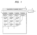
- Fig. 1 is a schematic view showing a solid-state image pickup element according to the first embodiment of the present invention.
- Object light is photoelectrically converted by photodiodes (PDs) 1 each serving as a photoelectric conversion unit.
- the photodiodes 1 are arrayed in a matrix form as pixels P 11 , P 12 , P 13 ,..., P 21 , P 22 , P 23 ,..., P 31 , P 32 , P 33 ,....
- Charges photoelectrically converted by the photodiodes 1 are transferred to vertical CCDs 2 through transfer gates.
- the charges transferred to the vertical CCDs 2 are transferred to charge detection circuits 3 and converted into a voltage at once every horizontal period.
- the interline CCD unit is formed from the photodiodes 1 and vertical CCDs 2. Unlike the conventional interline CCD shown in Fig. 11, signal charges from the vertical CCDs are transferred (not to the horizontal CCD) to the charge detection circuits 3.
- the signal voltage is output to a horizontal signal line 5 in accordance with a pulse from a horizontal scanning circuit 4 and guided to an image signal processing circuit (not shown) on the output side through an output amplifier 6.
- the output signal from each charge detection circuit 3 may be directly read out.
- a signal processing means for executing signal processing such as noise removal or A/D conversion may be provided on the output side of each charge detection circuit 3 and the signal may be output by the horizontal scanning circuit 4.
- the solid-state image pickup element shown in Fig. 1 is formed on a single semiconductor chip.
- Fig. 2 is a schematic view of the charge detection circuit and signal processing circuit shown in Fig. 1.
- the charge detection circuit comprises a charge detection amplifier (FD-Amp; floating diffusion amplifier) having a gate to which signal charges from the vertical CCD are transferred, and a reset transistor TR for resetting the gate of the charge detection amplifier.
- the signal processing circuit comprises a clamp capacitor Cp for removing noise, a transistor Tp, storage capacitors C S1 and C S2 for storing signals after noise removal, transfer transistors T S1 and T S2 for connecting the clamp capacitor Cp to the storage capacitors C S1 and C S2 , and transistors T C1 and T C2 for outputting signals from the storage capacitors C S1 and C S2 to horizontal signal lines 5 1 and 5 2 .
- These components form a charge detection/signal processing block 100.
- the vertical CCD 2 transfers charges to the charge detection amplifier (FD-Amp; floating diffusion amplifier) through a transfer gate TG every horizontal period in accordance with a drive pulse ⁇ Vn.
- the charge detection amplifier (FD-Amp) reset noise is generated by a parasitic capacitance and the reset transistor TR for removing residual voltage (charges) in the gate unit.
- the offset voltage fluctuates among the charge detection amplifiers (FD-Amps). To remove these noise components, the noise is clamped by the clamp capacitor Cp before the charges are transferred from the vertical CCD 2 to the charge detection amplifier (FD-Amp).
- the transfer gate TG is turned on to transfer the charges in the vertical CCD 2 (signal charges from the pixels P 11 , P 12 , P 13 ,...) to the gate unit of the charge detection amplifier (FD-Amp) and converted into a voltage by its parasitic capacitance.
- the above-described reset noise and offset voltage are superposed on the output signal voltage from the charge detection amplifier. Since the noise components are clamped by the clamp capacitor Cp, the noise is consequently removed at the output terminal of the clamp capacitor Cp, and only the signal voltage is stored in the storage capacitor C S1 .
- next charges in the vertical CCD 2 (signal charges from the pixels P 21 , P 22 , P 23 , ...) are converted into a voltage and, after noise removal, stored in the storage capacitor C S2 .
- Pixel signals S 01 and S 02 of two rows which are stored in the storage capacitors C S1 and C S2 are sequentially transferred to the horizontal signal lines 5 1 and 5 2 in accordance with a scanning pulse from the horizontal scanning circuit 4.
- Fig. 3 is an operation timing chart of the charge detection circuit and signal processing circuit shown in Fig. 2.
- the drive pulse ⁇ Vn goes high during a period T 1 to transfer charges to the vertical CCD 2 on the input side of the transfer gate TG.
- a power supply voltage Vcc of the charge detection amplifier (FD-Amp) is applied, a signal ⁇ C goes high to reset the gate of the charge detection amplifier (FD-Amp), a signal ⁇ P goes high to turn on the transistor Tp, the output terminal of the clamp capacitor Cp is clamped to the reference voltage, and signals ⁇ S1 and ⁇ S2 go high to reset the residual charges in the storage capacitors C S1 and C S2 .
- reset noise and offset voltage components are clamped by the clamp capacitor Cp.
- a signal ⁇ T goes high to turn on the transfer gate TG and transfer the signal charges to the gate portion of the charge detection amplifier.
- the above-described reset noise and offset voltage are superposed on the output signal voltage from the charge detection amplifier.
- the noise is consequently removed at the output terminal of the clamp capacitor Cp, and the signal ⁇ S1 goes high, so that the pixel signal of a row V 1 , from which noise has been removed, is stored in the storage capacitor C S1 .
- the power supply voltage Vcc of the charge detection amplifier is turned off to prevent power consumption.
- the charge detection amplifier operates at a low speed in one horizontal scanning period, the frequency bandwidth is small. For this reason, noise generated in the amplifier is much smaller than in the output amplifier of a general CCD.
- CDS noise removing operation
- the time required for reset operation of the FD-Amp and charge transfer from the vertical CCD is preferably short.
- the signals stored in the storage capacitors C S1 and C S2 are sequentially output during a next period T 6 in accordance with a scanning pulse ⁇ Hmn ( ⁇ H 01 , ⁇ H 02 , ⁇ H 03 ,...) from the horizontal scanning circuit 4. That is, since the signal is selected and output on the each pixel signal basis, the power consumption of the horizontal scanning circuit is low. In addition, since pixel signals of two rows can be simultaneously output, high-speed drive can be performed. If drive at a higher speed is necessary, the number of memories (storage capacitors) is increased to execute multiple-line output.
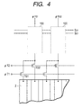
- Fig. 4 shows a solid-state image pickup element according to the second embodiment of the present invention. Circuits in a charge detection/signal processing block 100, which are identical to those in Fig. 2, are not illustrated in Fig. 4.
- charges in a plurality of vertical CCDs 2 are sequentially output using a common charge detection amplifier.
- Signals ⁇ T1 and ⁇ T2 are sequentially set to H level to turn on transfer gates T G1 and T G2 to sequentially control charge transfer from vertical CCDs of two columns to the charge detection amplifier whereby pixel signals of two columns are stored in storage capacitors C S1 and C S2 and output.
- the charge detection circuit and signal processing circuit can be formed in the width of two pixels, the chip area can be decreased.
- the signal processing circuit can have a programmable gain amplifier, A/D conversion circuit, and for a color sensor, a white balance circuit, and the like.
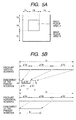
- Figs. 5A and 5B are explanatory views of the third embodiment related to random access drive.
- This embodiment has the same arrangement as described above except a horizontal scanning circuit 4, and as its characteristic feature, the solid-state image pickup element is a random-accessible solid-state image pickup element.
- Fig. 5A is a view showing an image pickup surface
- Fig. 5B is a timing chart of an image read from an image pickup area A.
- An image pickup area includes the image pickup areas A and B.
- drive is performed using almost the same frequency for both the vertical and horizontal scanning periods.
- high-speed drive can be performed when only the image pickup area A that should be read out is read out.
- the conventional CCD it is difficult to read out the image pickup area A to be read out at a high speed.
- the vertical CCD is driven at a high speed to remove unnecessary charges by a reset transistor TR of the charge detection amplifier.
- a random-accessible horizontal scanning circuit is arranged to execute scanning to output a signal only during a period H B .
- a decoder or a shift register which is divided into a plurality of areas and can start on each area basis is used. As a result, only the image signal in the image pickup area A can be read out. For this reason, high-speed drive can be achieved, and the power consumption can be reduced because the unnecessary image pickup area is not driven.
- More developed random access can be realized by a CCD capable of selecting a pixel row.
- a CCD capable of selecting a pixel row.
- an element is disclosed in the Institute of Image Information and Television Engineers technical report TEBS 101-6 ED 841.
- This known example is called a charge sweep device in which pixel row selection is driven by a vertical TG-SCANNER.
- the technological advantages of this embodiment can be expected.
- FIG. 6 is a block diagram of an equivalent circuit having a charge detection circuit and sequential-comparison-type A/D conversion circuit unit.
- a D/A converter receives DA output range switching information used to switch the range of the ramp-shaped reference voltage.
- the circuit comprises a vertical CCD 2, a transfer gate 42 for transferring signal charges from the vertical CCD 2 to the gate of an FD-Amp (floating diffusion amplifier) 43, a selection transistor 44, a reset transistor 45, a current supply transistor 46 for storing, as a voltage, the output current from the FD-Amp 43 by a switch 47 and storage capacitor 48 and outputting the voltage while converting it into a current, a comparator 51 for detecting the difference between the output current from the current supply transistor 46 and the output current from the FD-Amp 43 through the selection transistor 44, a counter 50 for counting the output from the comparator 51, and a D/A converter 49 for outputting a voltage to the source (main electrode) terminal of the FD-Amp 43 in accordance with a digital signal output from the counter 50.
- the D/A converter 49 receives DA output range switching information to switch the range of the ramp-shaped reference voltage to be output from the D/A converter 49 such that the pixel signal has an optimum value within the
- a method of obtaining a signal voltage by signal charges from the vertical CCD after the FD-Amp is reset in the above arrangement will be described as an example with reference to the timing chart shown in Fig. 7.
- the description below will be made while assuming that the transistors 42, 43, 44, and 45 shown in Fig. 6 are PMOS transistors, and the transistor 46 is an NMOS transistor.
- the D/A converter 49 is set to output a high potential (V HD ). Assume that the counter 50 is reset and no count operation is being performed.
- a signal ⁇ c is set to "L" level (pulse 201) to turn on the reset transistor 45 to reset the gate terminal of the FD-Amp 43 to a predetermined potential.
- a signal ⁇ x is set to "L" level (pulse 202) to turn on the selection transistor 44 and also turn on the switch 47.
- the output current from the FD-Amp 43 at the time of reset is stored in the storage capacitor 48 as a gate voltage generated when the gate and drain of the transistor 46 short-circuit (the comparison reference voltage is stored).
- the transistors 45 and 44 and switch 47 are turned off, and a signal ⁇ T is set to "L" level (pulse 203) to turn on the transfer gate 42 to transfer signal charges from the vertical CCD to the gate terminal of the FD-Amp 43.
- the output current from the FD-Amp 43 has a larger value than at the time of reset.
- the transistor 46 receives the voltage from the storage capacitor 48 and outputs the current when the FD-Amp 43 is reset.
- the signal ⁇ X is set to "L" level (pulse 204) to turn on the transistor 44 again, the input potential of the comparator 51 rises to a high potential (V H ).
- the counter 50 is operated, and its digital output is amplified.
- the output voltage from the D/A converter 49 that receives the output from the counter 50 gradually decreases (assume that the D/A converter 49 generates a negative analog output voltage with respect to the digital input signal).
- the output current from the FD-Amp 43 becomes equal to that from the transistor 46, and the input voltage to the comparator 51 abruptly decreases.
- the count operation of the counter 50 is stopped.
- the digital value that has changed during a period from the start to the end of counting by the counter 50 equals to the difference between the gate potential of the FD-Amp 43 at the time of reset and the potential when the signal charges are transferred. In this way, A/D conversion is executed correspondingly to the difference.
- Fig. 8 is a schematic circuit diagram showing connection between the vertical CCD and the charge detection circuit and A/D conversion circuit.
- the same reference numerals as in Fig. 6 denote the same members in Fig. 8.
- the signal charges from the vertical CCD 2 are input to the gate of the FD-Amp 43, converted into digital data by the counter 50, sequentially selected by a data selector 52, and output as A/D-converted data.
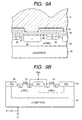
- Figs. 9A and 9B are sectional views showing the structure of a solid-state image pickup element according to the fifth embodiment.
- Fig. 9A is a sectional view showing the structure of a photoelectric conversion unit, vertical CCD, and channel stop.
- Fig. 9B is a sectional view showing the structure of an inverter unit that forms part of a signal processing circuit.
- a unit pixel is formed from a PD region serving as a photoelectric conversion unit, a transfer gate region for transferring charges, a vertical CCD region, and a channel stop region. These regions are formed in a p-well 65 formed on an n-substrate 60. In the PD region, a dark current is reduced by a p + -layer 67 on the surface. In the vertical CCD region, a p-layer 68 is formed under an n-layer 69 to reduce an increase and smearing in transfer charge amount. In the transfer gate region, control is executed to transfer photocharges from the PD to the vertical CCD.
- the solid-state image pickup element also has a microlens 61 for focusing light in the PD region, a light-shielding layer 62, a gate electrode 63 made of polysilicon, and an SiO 2 layer 64.
- a p-well and n-well are formed on the n-substrate 60 to form an NMOS transistor and PMOS transistor.
- Well separation between the CCD unit and the signal processing circuit unit is preferably done from the charge detection circuit unit. This is because the signal processing circuit unit generates pulse noise due to high-speed signal transfer or the logic circuit. To prevent noise from propagating from the noise source to the CCD unit, the CCD unit and signal processing circuit are separated by the well.
- the charge detection circuit unit may be formed in the CCD well. Since the charge detection circuit unit has a function of converting signal charges into a voltage every horizontal period and therefore operates at a low speed, it generates little noise.
- Fig. 13 shows a structure in which the inverter unit is separated by a deep well. When the inverter unit is completely separated from the sensor unit, noise from the inverter unit can be more effectively shielded.
- the solid-state image pickup element of this embodiment can have any one of the equivalent circuits of the first to fourth embodiments.
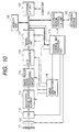
- the camera has a barrier 111 serving as the protection and main switch of a lens, a lens 112 for forming an optical image of an object onto a solid-state image pickup element 114, an iris 113 for changing the amount of light transmitted through the lens 112, the solid-state image pickup element 114 for receiving the object image formed by the lens 112 to output an image signal, an image pickup signal processing circuit 115, an A/D converter 116 for executing A/D conversion of the image signal output from the image pickup signal processing circuit 115, a signal processing unit 117 for executing various kinds of correction operations for the image data output from the A/D converter 116 or compressing the data, a timing generation unit 118 for outputting various kinds of timing signals to the solid-state image pickup element 114, image pickup signal processing circuit 115, A/D converter 116, and signal processing unit 117, a system control and operation unit 119 for executing various kinds of operations and controlling the entire still video camera, a memory unit 120 for temporarily storing the image data, an interface
- the system control and operation unit 119 sets the iris 113 in the full-aperture state.
- the signal output from the solid-state image pickup element 114 is converted by the A/D converter 116 and input to the signal processing unit 117.
- the system control and operation unit 119 executes calculation for exposure on the basis of the data.
- the brightness is determined on the basis of the result of photometry, and in accordance with the result, the system control and operation unit 119 controls the iris.
- the lens On the basis of the signal output from the solid-state image pickup element 114, a high-frequency component is extracted, and the distance to the object is calculated by the system control and operation unit 119. After that, the lens is driven, and it is determined whether an in-focus state is obtained. If it is determined that no in-focus state is obtained, the lens is driven again, and distance measurement is performed. After confirming the in-focus state, actual exposure starts.
- the image signal output from the solid-state image pickup element 114 is A/D-converted by the A/D converter 116, passes through the signal processing unit 117, and is written in the memory unit by the system control and operation unit 119.
- the data stored in the memory unit 120 is recorded on the detachable recording medium 122 such as a semiconductor memory through the recording medium control I/F unit 121 under the control of the system control and operation unit 119.
- the image data may be directly input to a computer or the like through the external I/F unit 123 to process the image.
- a sensitive image pickup apparatus capable of high-performance function, high-speed drive, and power consumption reduction can be provided.
Landscapes
- Engineering & Computer Science (AREA)
- Multimedia (AREA)
- Signal Processing (AREA)
- Solid State Image Pick-Up Elements (AREA)
- Transforming Light Signals Into Electric Signals (AREA)
Abstract
Description
- The present invention relates to an image pickup apparatus for picking up an object image.
- Conventional solid-state image pickup elements are mainly classified into CCD-type elements and CMOS-type elements. Examples of CCD-type elements are an interline CCD (IL-CCD) and frame transfer CCD (FT-CCD).
- An interline CCD comprises a plurality of photoelectric conversion units, vertical CCDs, transfer gates for transferring signal charges in the photoelectric conversion units to the vertical CCDs, a horizontal CCD for horizontally transferring the charges from the vertical CCDs, and a floating diffusion amplifier (FD-Amp). A frame transfer CCD comprises photoelectric conversion units, a storage unit to which charges in the photoelectric conversion units are transferred (frame-shifted), a horizontal transfer unit for horizontally transferring the charges from the storage unit, and a floating diffusion amplifier (FD-Amp). Fig. 11 shows an IL-CCD as a typical example of a CCD-type solid-state image pickup element.
- As shown in Fig. 11, an IL-CCD comprises photoelectric conversion units (PDs) 70, vertical CCDs (V-CCDs) 71 for temporarily storing charges from the
photoelectric conversion units 70, a horizontal CCD (H-CCD) 72 for receiving the charges from thevertical CCDs 71 and transferring the charges in the horizontal direction, and a floating diffusion amplifier (FD-Amp) 73 serving as an output amplifier for converting the charges from thehorizontal CCD 72 into a voltage. - The CCD has low noise level because signal charges are completely transferred to the FD-Amp on the output side. In addition, the pixel size can be made small because of the simple pixel structure. Today, however, the number of pixels in a sensor for a digital camera reaches several millions for higher quality, and high-speed drive is indispensable in an HD camera. For this reason, the power consumption of a horizontal CCD drive circuit is high (up to CfV2). Although a CDS circuit for reducing reset noise in an FD-Amp requires a sampling accuracy on the order of nsec, that sampling accuracy cannot be ensured because of the mass production and the wide range of use conditions (temperature and a variation in voltage). Hence, a low-noise CCD can hardly be implemented.
- In a CMOS sensor, as shown in Fig. 12, each
pixel unit 80 comprises a photoelectric conversion unit PD and a MOS transistor serving as a pixel amplifier. The pixels are selected and driven by a random-accessiblevertical scanning circuit 81 andhorizontal scanning circuit 85, resulting in functional advantage. Charges in eachpixel unit 80 are converted into a voltage by the pixel amplifier, output to aclamp circuit 83 through avertical signal line 82, and after noise removal from the pixel unit amplifier by theclamp circuit 83, output to ahorizontal signal line 84. The signals are sequentially output by thehorizontal scanning circuit 85 from thehorizontal signal line 84 through an amplifier (Amp) 86. Since a CMOS sensor sequentially selects and outputs each pixel signal by thehorizontal scanning circuit 85, unlike charge transfer as in a CCD, the power consumption is low. However, since the number of elements of each pixel unit is large, it is difficult to reduce the pixel size. - As described above, a CCD is advantageous in increasing the number of pixels but disadvantageous in high-speed drive and power consumption. Conversely, a CMOS sensor is disadvantageous in increasing the number of pixels but advantageous in high-speed drive and power consumption.
- It is an object of the present invention to provide an image pickup apparatus suitable to increase the number of pixels and capable of high-performance function, power consumption reduction, and high-speed drive.
- In order to achieve the above object, according to an aspect of the present invention, there is provided an image pickup apparatus comprising:
- a solid-state image pickup element formed on a
single semiconductor chip, the solid-state image pickup
element including:
- photoelectric conversion units arranged two-dimensionally;
- a plurality of CCDs adapted to transfer charges generated by the photoelectric conversion units arranged two-dimensionally, each of the plurality of CCDs being arranged correspondingly to each line of photoelectric conversion units;
- a plurality of charge detection circuits adapted to detect the charges from the plurality of CCDs and supplying corresponding signal levels, each of the plurality of charge detection circuits being arranged correspondingly to each CCD;
- a common output line to which signals from the plurality of charge detection circuits are sequentially output;
- a plurality of transfer transistors adapted to transfer the signals from the plurality of charge detection circuits to the common output line; and
- a scanning circuit adapted to control the plurality of transfer transistors to sequentially output the signals from the plurality of charge detection circuits to the common output line.
-
- According to another aspect of the present invention, there is provided an image pickup apparatus comprising:
- a solid-state image pickup element formed on a
single semiconductor chip, the solid-state image pickup
element including:
- photoelectric conversion units arranged two-dimensionally;
- a plurality of CCDs adapted to transfer charges generated by the photoelectric conversion units, each of the plurality of CCDs being arranged correspondingly to each line of photoelectric conversion units;
- a plurality of charge detection circuits adapted to detect the charges from the CCDs and supplying corresponding-signal levels, each of the plurality of charge detection circuits being arranged correspondingly to each CCD; and
- a plurality of A/D conversion circuits adapted to convert the signals from the charge detection circuits into digital signals, each of the A/D conversion circuits being arranged correspondgly to each charge detection circuit.
-
- The above and other objects, features, and advantages of the present invention will become apparent from the following description in conjunction with the accompanying drawings.
-
- Fig. 1 is a schematic view showing a solid-state image pickup element according to the first embodiment of the present invention;
- Fig. 2 is a schematic view of a charge detection circuit and signal processing circuit shown in Fig. 1;
- Fig. 3 is an operation timing chart of the charge detection circuit and signal processing circuit shown in Fig. 2;
- Fig. 4 is a view showing a solid-state image pickup element according to the second embodiment of the present invention;
- Figs. 5A and 5B are explanatory views of random access drive according to the third embodiment of the present invention;
- Fig. 6 is a block diagram of an equivalent circuit having a charge detection circuit and A/D conversion circuit unit according to the fourth embodiment of the present invention;
- Fig. 7 is a timing chart for explaining the operation shown in Fig. 6;
- Fig. 8 is a schematic circuit diagram showing connection between a vertical CCD and a charge detection circuit and A/D conversion circuit according to the fourth embodiment of the present invention;
- Figs. 9A and 9B are sectional views showing the structure of a solid-state image pickup element according to the fifth embodiment of the present invention;
- Fig. 10 is a block diagram showing a case wherein the solid-state image pickup element of any one of the first to fifth embodiments is applied to a "digital still camera";
- Fig. 11 is a schematic view of an IL-CCD;
- Fig. 12 is a schematic view of a CMOS sensor; and
- Fig. 13 is a view showing a structure in which an inverter unit is separated by a deep well.
-
- The embodiments of the present invention will be described below in detail with reference to the accompanying drawings. An arrangement using an interline CCD (IL-CCD) will be described here. The present invention can also be applied to a frame transfer CCD. In that case, charges from a storage unit are output to a charge detection circuit.
- Fig. 1 is a schematic view showing a solid-state image pickup element according to the first embodiment of the present invention. Object light is photoelectrically converted by photodiodes (PDs) 1 each serving as a photoelectric conversion unit. The
photodiodes 1 are arrayed in a matrix form as pixels P11, P12, P13,..., P21, P22, P23,..., P31, P32, P33,.... Charges photoelectrically converted by thephotodiodes 1 are transferred tovertical CCDs 2 through transfer gates. The charges transferred to thevertical CCDs 2 are transferred to chargedetection circuits 3 and converted into a voltage at once every horizontal period. The interline CCD unit is formed from thephotodiodes 1 andvertical CCDs 2. Unlike the conventional interline CCD shown in Fig. 11, signal charges from the vertical CCDs are transferred (not to the horizontal CCD) to thecharge detection circuits 3. - The signal voltage is output to a
horizontal signal line 5 in accordance with a pulse from ahorizontal scanning circuit 4 and guided to an image signal processing circuit (not shown) on the output side through anoutput amplifier 6. - The output signal from each
charge detection circuit 3 may be directly read out. Alternatively, a signal processing means for executing signal processing such as noise removal or A/D conversion may be provided on the output side of eachcharge detection circuit 3 and the signal may be output by thehorizontal scanning circuit 4. - The solid-state image pickup element shown in Fig. 1 is formed on a single semiconductor chip.
- Fig. 2 is a schematic view of the charge detection circuit and signal processing circuit shown in Fig. 1. The charge detection circuit comprises a charge detection amplifier (FD-Amp; floating diffusion amplifier) having a gate to which signal charges from the vertical CCD are transferred, and a reset transistor TR for resetting the gate of the charge detection amplifier. The signal processing circuit comprises a clamp capacitor Cp for removing noise, a transistor Tp, storage capacitors CS1 and CS2 for storing signals after noise removal, transfer transistors TS1 and TS2 for connecting the clamp capacitor Cp to the storage capacitors CS1 and CS2, and transistors TC1 and TC2 for outputting signals from the storage capacitors CS1 and CS2 to
horizontal signal lines signal processing block 100. - The
vertical CCD 2 transfers charges to the charge detection amplifier (FD-Amp; floating diffusion amplifier) through a transfer gate TG every horizontal period in accordance with a drive pulse Vn. In the charge detection amplifier (FD-Amp), reset noise is generated by a parasitic capacitance and the reset transistor TR for removing residual voltage (charges) in the gate unit. In addition, the offset voltage fluctuates among the charge detection amplifiers (FD-Amps). To remove these noise components, the noise is clamped by the clamp capacitor Cp before the charges are transferred from thevertical CCD 2 to the charge detection amplifier (FD-Amp). - After this clamp, the transfer gate TG is turned on to transfer the charges in the vertical CCD 2 (signal charges from the pixels P11, P12, P13,...) to the gate unit of the charge detection amplifier (FD-Amp) and converted into a voltage by its parasitic capacitance. The above-described reset noise and offset voltage are superposed on the output signal voltage from the charge detection amplifier. Since the noise components are clamped by the clamp capacitor Cp, the noise is consequently removed at the output terminal of the clamp capacitor Cp, and only the signal voltage is stored in the storage capacitor CS1.
- With the same operation, the next charges in the vertical CCD 2 (signal charges from the pixels P21, P22, P23, ...) are converted into a voltage and, after noise removal, stored in the storage capacitor CS2. Pixel signals S01 and S02 of two rows which are stored in the storage capacitors CS1 and CS2 are sequentially transferred to the
horizontal signal lines horizontal scanning circuit 4. - Fig. 3 is an operation timing chart of the charge detection circuit and signal processing circuit shown in Fig. 2.
- As shown in Fig. 3, first, the drive pulse Vn goes high during a period T1 to transfer charges to the
vertical CCD 2 on the input side of the transfer gate TG. During a period T2, a power supply voltage Vcc of the charge detection amplifier (FD-Amp) is applied, a signal C goes high to reset the gate of the charge detection amplifier (FD-Amp), a signal P goes high to turn on the transistor Tp, the output terminal of the clamp capacitor Cp is clamped to the reference voltage, and signals S1 and S2 go high to reset the residual charges in the storage capacitors CS1 and CS2. At this time, reset noise and offset voltage components are clamped by the clamp capacitor Cp. - During a period T3, a signal T goes high to turn on the transfer gate TG and transfer the signal charges to the gate portion of the charge detection amplifier. The above-described reset noise and offset voltage are superposed on the output signal voltage from the charge detection amplifier. However, the noise is consequently removed at the output terminal of the clamp capacitor Cp, and the signal S1 goes high, so that the pixel signal of a row V1, from which noise has been removed, is stored in the storage capacitor CS1.
- During periods T4 and T5, with the same operation as in the periods T2 and T3, charges in the
vertical CCD 2 are transferred to the next cell. In a state wherein the power supply voltage Vcc of the charge detection amplifier (FD-Amp) is applied, the signal C goes high to reset the gate of the charge detection amplifier (FD-Amp), and the signal P goes high to clamp the output terminal of the clamp capacitor Cp to the reference voltage. The signals T and S2 go high so that the pixel signal of a row V2, from which noise has been removed, is stored in the storage capacitor CS2. - After the end of the period T5, the power supply voltage Vcc of the charge detection amplifier is turned off to prevent power consumption.
- As described above, since the charge detection amplifier operates at a low speed in one horizontal scanning period, the frequency bandwidth is small. For this reason, noise generated in the amplifier is much smaller than in the output amplifier of a general CCD. In addition, because of low-frequency drive, no problem is posed in noise removing operation (CDS), i.e., clamp operation. To increase the 1/f noise reduction effect of the FD-Amp, the time required for reset operation of the FD-Amp and charge transfer from the vertical CCD is preferably short.
- The signals stored in the storage capacitors CS1 and CS2 are sequentially output during a next period T6 in accordance with a scanning pulse Hmn (H01, H02, H03,...) from the
horizontal scanning circuit 4. That is, since the signal is selected and output on the each pixel signal basis, the power consumption of the horizontal scanning circuit is low. In addition, since pixel signals of two rows can be simultaneously output, high-speed drive can be performed. If drive at a higher speed is necessary, the number of memories (storage capacitors) is increased to execute multiple-line output. - Fig. 4 shows a solid-state image pickup element according to the second embodiment of the present invention. Circuits in a charge detection/
signal processing block 100, which are identical to those in Fig. 2, are not illustrated in Fig. 4. - In this embodiment, charges in a plurality of
vertical CCDs 2 are sequentially output using a common charge detection amplifier. Signals T1 and T2 are sequentially set to H level to turn on transfer gates TG1 and TG2 to sequentially control charge transfer from vertical CCDs of two columns to the charge detection amplifier whereby pixel signals of two columns are stored in storage capacitors CS1 and CS2 and output. In this embodiment, since the charge detection circuit and signal processing circuit can be formed in the width of two pixels, the chip area can be decreased. - The signal processing circuit can have a programmable gain amplifier, A/D conversion circuit, and for a color sensor, a white balance circuit, and the like.
- Figs. 5A and 5B are explanatory views of the third embodiment related to random access drive. This embodiment has the same arrangement as described above except a
horizontal scanning circuit 4, and as its characteristic feature, the solid-state image pickup element is a random-accessible solid-state image pickup element. Fig. 5A is a view showing an image pickup surface, and Fig. 5B is a timing chart of an image read from an image pickup area A. - An image pickup area includes the image pickup areas A and B. In the prior art, drive is performed using almost the same frequency for both the vertical and horizontal scanning periods. In fact, high-speed drive can be performed when only the image pickup area A that should be read out is read out. In the conventional CCD, it is difficult to read out the image pickup area A to be read out at a high speed. In the embodiment of the present invention, during an unnecessary image pickup period VA (VC) in the vertical direction, the vertical CCD is driven at a high speed to remove unnecessary charges by a reset transistor TR of the charge detection amplifier. During an unnecessary image pickup period HA (HC) in the horizontal direction, a random-accessible horizontal scanning circuit is arranged to execute scanning to output a signal only during a period HB. That is, a decoder or a shift register which is divided into a plurality of areas and can start on each area basis is used. As a result, only the image signal in the image pickup area A can be read out. For this reason, high-speed drive can be achieved, and the power consumption can be reduced because the unnecessary image pickup area is not driven.
- More developed random access can be realized by a CCD capable of selecting a pixel row. As a known example, an element is disclosed in the Institute of Image Information and Television Engineers technical report TEBS 101-6 ED 841. This known example is called a charge sweep device in which pixel row selection is driven by a vertical TG-SCANNER. When such a charge sweep device and the charge detection amplifier and signal processing circuit according to this embodiment are combined, the technological advantages of this embodiment can be expected.
- As a characteristic feature of the fourth embodiment, an A/D conversion circuit unit is prepared for each column. Fig. 6 is a block diagram of an equivalent circuit having a charge detection circuit and sequential-comparison-type A/D conversion circuit unit. A D/A converter receives DA output range switching information used to switch the range of the ramp-shaped reference voltage.
- Referring to Fig. 6, the circuit comprises a
vertical CCD 2, atransfer gate 42 for transferring signal charges from thevertical CCD 2 to the gate of an FD-Amp (floating diffusion amplifier) 43, aselection transistor 44, areset transistor 45, acurrent supply transistor 46 for storing, as a voltage, the output current from the FD-Amp 43 by aswitch 47 andstorage capacitor 48 and outputting the voltage while converting it into a current, acomparator 51 for detecting the difference between the output current from thecurrent supply transistor 46 and the output current from the FD-Amp 43 through theselection transistor 44, acounter 50 for counting the output from thecomparator 51, and a D/A converter 49 for outputting a voltage to the source (main electrode) terminal of the FD-Amp 43 in accordance with a digital signal output from thecounter 50. The D/A converter 49 receives DA output range switching information to switch the range of the ramp-shaped reference voltage to be output from the D/A converter 49 such that the pixel signal has an optimum value within the A/D input voltage range. - A method of obtaining a signal voltage by signal charges from the vertical CCD after the FD-Amp is reset in the above arrangement will be described as an example with reference to the timing chart shown in Fig. 7. The description below will be made while assuming that the
transistors transistor 46 is an NMOS transistor. The D/A converter 49 is set to output a high potential (VHD). Assume that thecounter 50 is reset and no count operation is being performed. A signal c is set to "L" level (pulse 201) to turn on thereset transistor 45 to reset the gate terminal of the FD-Amp 43 to a predetermined potential. Simultaneously, a signal x is set to "L" level (pulse 202) to turn on theselection transistor 44 and also turn on theswitch 47. The output current from the FD-Amp 43 at the time of reset is stored in thestorage capacitor 48 as a gate voltage generated when the gate and drain of thetransistor 46 short-circuit (the comparison reference voltage is stored). After that, thetransistors transfer gate 42 to transfer signal charges from the vertical CCD to the gate terminal of the FD-Amp 43. If the gate potential at this time is lower than that at the time of reset, the output current from the FD-Amp 43 has a larger value than at the time of reset. Thetransistor 46 receives the voltage from thestorage capacitor 48 and outputs the current when the FD-Amp 43 is reset. When the signal X is set to "L" level (pulse 204) to turn on thetransistor 44 again, the input potential of thecomparator 51 rises to a high potential (VH). After that, thecounter 50 is operated, and its digital output is amplified. The output voltage from the D/A converter 49 that receives the output from thecounter 50 gradually decreases (assume that the D/A converter 49 generates a negative analog output voltage with respect to the digital input signal). At certain time, the output current from the FD-Amp 43 becomes equal to that from thetransistor 46, and the input voltage to thecomparator 51 abruptly decreases. Upon detecting that change, the count operation of thecounter 50 is stopped. - The digital value that has changed during a period from the start to the end of counting by the
counter 50 equals to the difference between the gate potential of the FD-Amp 43 at the time of reset and the potential when the signal charges are transferred. In this way, A/D conversion is executed correspondingly to the difference. - Fig. 8 is a schematic circuit diagram showing connection between the vertical CCD and the charge detection circuit and A/D conversion circuit. The same reference numerals as in Fig. 6 denote the same members in Fig. 8.
- The signal charges from the
vertical CCD 2 are input to the gate of the FD-Amp 43, converted into digital data by thecounter 50, sequentially selected by adata selector 52, and output as A/D-converted data. - Figs. 9A and 9B are sectional views showing the structure of a solid-state image pickup element according to the fifth embodiment. Fig. 9A is a sectional view showing the structure of a photoelectric conversion unit, vertical CCD, and channel stop. Fig. 9B is a sectional view showing the structure of an inverter unit that forms part of a signal processing circuit.
- As shown in Fig. 9A, a unit pixel is formed from a PD region serving as a photoelectric conversion unit, a transfer gate region for transferring charges, a vertical CCD region, and a channel stop region. These regions are formed in a p-well 65 formed on an n-
substrate 60. In the PD region, a dark current is reduced by a p+-layer 67 on the surface. In the vertical CCD region, a p-layer 68 is formed under an n-layer 69 to reduce an increase and smearing in transfer charge amount. In the transfer gate region, control is executed to transfer photocharges from the PD to the vertical CCD. The solid-state image pickup element also has amicrolens 61 for focusing light in the PD region, a light-shielding layer 62, agate electrode 63 made of polysilicon, and an SiO2 layer 64. - As shown in Fig. 9B, in the inverter unit as part of the signal processing circuit, a p-well and n-well are formed on the n-
substrate 60 to form an NMOS transistor and PMOS transistor. - Well separation between the CCD unit and the signal processing circuit unit is preferably done from the charge detection circuit unit. This is because the signal processing circuit unit generates pulse noise due to high-speed signal transfer or the logic circuit. To prevent noise from propagating from the noise source to the CCD unit, the CCD unit and signal processing circuit are separated by the well. For some application purposes, the charge detection circuit unit may be formed in the CCD well. Since the charge detection circuit unit has a function of converting signal charges into a voltage every horizontal period and therefore operates at a low speed, it generates little noise. Fig. 13 shows a structure in which the inverter unit is separated by a deep well. When the inverter unit is completely separated from the sensor unit, noise from the inverter unit can be more effectively shielded. The solid-state image pickup element of this embodiment can have any one of the equivalent circuits of the first to fourth embodiments.
- The sixth embodiment wherein the solid-state image pickup element of any one of the above-described first to fourth embodiments is applied to a digital still camera (image pickup apparatus) will be described in detail with reference to Fig. 10.
- Referring to Fig. 10, the camera has a barrier 111 serving as the protection and main switch of a lens, a lens 112 for forming an optical image of an object onto a solid-state image pickup element 114, an iris 113 for changing the amount of light transmitted through the lens 112, the solid-state image pickup element 114 for receiving the object image formed by the lens 112 to output an image signal, an image pickup signal processing circuit 115, an A/D converter 116 for executing A/D conversion of the image signal output from the image pickup signal processing circuit 115, a signal processing unit 117 for executing various kinds of correction operations for the image data output from the A/D converter 116 or compressing the data, a timing generation unit 118 for outputting various kinds of timing signals to the solid-state image pickup element 114, image pickup signal processing circuit 115, A/D converter 116, and signal processing unit 117, a system control and operation unit 119 for executing various kinds of operations and controlling the entire still video camera, a memory unit 120 for temporarily storing the image data, an interface unit 121 for recording/reading out the image data on/from a recording medium, a detachable recording medium 122 such as a semiconductor memory for recording or reading out image data, and an interface unit 123 for communication with an external computer or the like.
- The operation of the still video camera with the above-described arrangement in the phototaking mode will be described next. When the
barrier 111 is opened, the main power supply is turned on, the power supply of the control system is turned on next, and finally, the power supply of the image pickup system circuit such as the A/D converter 116 is turned on. To control the exposure amount, the system control andoperation unit 119 sets theiris 113 in the full-aperture state. The signal output from the solid-stateimage pickup element 114 is converted by the A/D converter 116 and input to thesignal processing unit 117. The system control andoperation unit 119 executes calculation for exposure on the basis of the data. The brightness is determined on the basis of the result of photometry, and in accordance with the result, the system control andoperation unit 119 controls the iris. - On the basis of the signal output from the solid-state
image pickup element 114, a high-frequency component is extracted, and the distance to the object is calculated by the system control andoperation unit 119. After that, the lens is driven, and it is determined whether an in-focus state is obtained. If it is determined that no in-focus state is obtained, the lens is driven again, and distance measurement is performed. After confirming the in-focus state, actual exposure starts. - When exposure is ended, the image signal output from the solid-state
image pickup element 114 is A/D-converted by the A/D converter 116, passes through thesignal processing unit 117, and is written in the memory unit by the system control andoperation unit 119. - After that, the data stored in the
memory unit 120 is recorded on thedetachable recording medium 122 such as a semiconductor memory through the recording medium control I/F unit 121 under the control of the system control andoperation unit 119. The image data may be directly input to a computer or the like through the external I/F unit 123 to process the image. - As has been described above in detail, according to this embodiment, a sensitive image pickup apparatus capable of high-performance function, high-speed drive, and power consumption reduction can be provided.
- Many widely different embodiments of the present invention may be constructed without departing from the spirit and scope of the present invention. It should be understood that the present invention is not limited to the specific embodiments described in the specification, except as defined in the appended claims.
Claims (13)
- An image pickup apparatus comprising:a solid-state image pickup element formed on a single semiconductor chip, said solid-state image pickup element including:photoelectric conversion units arranged two-dimensionally;a plurality of CCDs adapted to transfer charges generated by said photoelectric conversion units arranged two-dimensionally, each of said plurality of CCDs being arranged correspondingly to each line of photoelectric conversion units;a plurality of charge detection circuits adapted to detect the charges from said plurality of CCDs and supplying corresponding signal levels, each of said plurality of charge detection circuits being arranged correspondingly to each CCD;a common output line to which signals from said plurality of charge detection circuits are sequentially output;a plurality of transfer transistors adapted to transfer the signals from said plurality of charge detection circuits to said common output line; anda scanning circuit adapted to control said plurality of transfer transistors to sequentially output the signals from said plurality of charge detection circuits to said common output line.
- An apparatus according to claim 1, further comprising a signal processing circuit inserted between said transfer transistor and said charge detection circuit.
- An apparatus according to claim 2, wherein said signal processing circuit includes a noise removing circuit adapted to remove a noise component contained in the signal output from said charge detection circuit.
- An apparatus according to claim 2, wherein said signal processing circuit includes a clamp circuit.
- An apparatus according to claim 1, further comprising a drive circuit adapted to drive said solid-state image pickup element so as to sweep at least a portion of unnecessary charges contained in said photoelectric conversion units arranged two-dimensionally, at input units of said plurality of charge detection circuits.
- An apparatus according to claim 1, wherein said charge detection circuit is provided in common to said plurality of CCDs and is connected to said plurality of CCDs through separate transistors.
- An apparatus according to claim 1, wherein said charge detection circuit comprises a control circuit adapted to execute control to supply power when an input unit of said charge detection circuit is reset and when the charges from said CCD are converted into a voltage and output.
- An apparatus according to claim 1, wherein said CCD and said charge detection circuit are separated by a well.
- An apparatus according to claim 1, further comprisinga lens adapted to form an image of light onto said solid-state image pickup element, anda signal processing circuit adapted to process a signal from said solid-state image pickup element.
- An image pickup apparatus comprising:a solid-state image pickup element formed on a single semiconductor chip, said solid-state image pickup element including:photoelectric conversion units arranged two-dimensionally;a plurality of CCDs adapted to transfer charges generated by said photoelectric conversion units, each of said plurality of CCDs being arranged correspondingly to each line of photoelectric conversion units;a plurality of charge detection circuits adapted to detect the charges from said CCDs and supplying corresponding signal levels, each of said plurality of charge detection circuits being arranged correspondingly to each CCD; anda plurality of A/D conversion circuits adapted to convert the signals from said charge detection circuits into digital signals, each of said A/D conversion circuits being arranged correspondingly to each charge detection circuit.
- An apparatus according to claim 10, wherein said A/D conversion circuit comprises a sequential-comparison-type circuit.
- An apparatus according to claim 10, further comprisinga lens adapted to form an image of light onto said solid-state image pickup element, anda signal processing circuit adapted to process a signal from said solid-state image pickup element.
- An apparatus according to claim 11, wherein said CCD and said charge detection circuit are separated by a well.
Applications Claiming Priority (2)
| Application Number | Priority Date | Filing Date | Title |
|---|---|---|---|
| JP2000324451 | 2000-10-24 | ||
| JP2000324451A JP3937716B2 (en) | 2000-10-24 | 2000-10-24 | Solid-state imaging device and imaging system |
Publications (2)
| Publication Number | Publication Date |
|---|---|
| EP1206127A2 true EP1206127A2 (en) | 2002-05-15 |
| EP1206127A3 EP1206127A3 (en) | 2009-08-05 |
Family
ID=18801984
Family Applications (1)
| Application Number | Title | Priority Date | Filing Date |
|---|---|---|---|
| EP01308976A Withdrawn EP1206127A3 (en) | 2000-10-24 | 2001-10-23 | Image pickup apparatus |
Country Status (3)
| Country | Link |
|---|---|
| US (2) | US7145600B2 (en) |
| EP (1) | EP1206127A3 (en) |
| JP (1) | JP3937716B2 (en) |
Families Citing this family (19)
| Publication number | Priority date | Publication date | Assignee | Title |
|---|---|---|---|---|
| JP4298964B2 (en) * | 2002-05-16 | 2009-07-22 | 富士フイルム株式会社 | Solid-state imaging device and manufacturing method thereof |
| JP2004266363A (en) * | 2003-02-18 | 2004-09-24 | Sony Corp | Imaging apparatus and driving method of imaging apparatus |
| JP2005101486A (en) * | 2003-08-28 | 2005-04-14 | Sanyo Electric Co Ltd | Solid-state imaging device and control method thereof |
| KR20050077434A (en) * | 2004-01-28 | 2005-08-02 | 삼성전자주식회사 | Image pickup device capable of reducing power consumption |
| JP4144535B2 (en) * | 2004-03-03 | 2008-09-03 | ソニー株式会社 | Solid-state imaging device and pixel signal readout method |
| JP4742523B2 (en) * | 2004-06-14 | 2011-08-10 | ソニー株式会社 | Solid-state imaging device and driving method thereof |
| JP2006041196A (en) * | 2004-07-27 | 2006-02-09 | Nec Electronics Corp | Solid-state imaging device and manufacturing method thereof |
| JP2006049986A (en) * | 2004-07-30 | 2006-02-16 | Sony Corp | Solid-state imaging device |
| US7923674B2 (en) * | 2005-06-29 | 2011-04-12 | National University Corporation NARA Institute of Science and Technology | Solid-state image sensor having a voltage applier and signal readout method thereof |
| JP4542962B2 (en) | 2005-07-21 | 2010-09-15 | 富士フイルム株式会社 | Digital camera |
| JP4740781B2 (en) * | 2006-03-30 | 2011-08-03 | 富士フイルム株式会社 | Solid-state imaging device |
| JP2008118434A (en) * | 2006-11-06 | 2008-05-22 | Fujifilm Corp | Solid-state imaging device and imaging apparatus |
| JPWO2008142968A1 (en) * | 2007-05-21 | 2010-08-05 | 株式会社島津製作所 | Image pickup device and image pickup apparatus including the same |
| JP5202395B2 (en) * | 2009-03-09 | 2013-06-05 | 株式会社半導体エネルギー研究所 | Touch panel, electronic equipment |
| JP5917883B2 (en) | 2011-11-02 | 2016-05-18 | 浜松ホトニクス株式会社 | Solid-state imaging device |
| JP5941659B2 (en) | 2011-11-02 | 2016-06-29 | 浜松ホトニクス株式会社 | Solid-state imaging device |
| JP5812959B2 (en) * | 2011-12-15 | 2015-11-17 | キヤノン株式会社 | Imaging device |
| JP5924924B2 (en) | 2011-12-15 | 2016-05-25 | キヤノン株式会社 | Electronic circuit |
| JP6623734B2 (en) * | 2015-12-14 | 2019-12-25 | セイコーエプソン株式会社 | Image reading device and semiconductor device |
Citations (3)
| Publication number | Priority date | Publication date | Assignee | Title |
|---|---|---|---|---|
| JPH0697414A (en) | 1992-09-11 | 1994-04-08 | Hitachi Ltd | Solid-state image sensing device |
| US5449908A (en) | 1993-12-30 | 1995-09-12 | Texas Instruments Incorporated | Hybrid CCD imaging |
| US5898509A (en) | 1996-10-15 | 1999-04-27 | Hewlett-Packard Company | Method for improving the signal-to-noise ratio of a CCD sensor in a color imaging device |
Family Cites Families (31)
| Publication number | Priority date | Publication date | Assignee | Title |
|---|---|---|---|---|
| US4985758A (en) * | 1982-12-07 | 1991-01-15 | Canon Kabushiki Kaisha | Signal processing system having selected output from plural readout devices |
| CA1269446A (en) * | 1984-12-28 | 1990-05-22 | Seiji Hashimoto | Image sensing apparatus |
| US4914519A (en) * | 1986-09-19 | 1990-04-03 | Canon Kabushiki Kaisha | Apparatus for eliminating noise in a solid-state image pickup device |
| EP0272152B1 (en) * | 1986-12-18 | 1994-08-03 | Canon Kabushiki Kaisha | Signal reading out circuit |
| EP0282993B1 (en) * | 1987-03-20 | 1994-02-02 | Canon Kabushiki Kaisha | Imaging apparatus |
| JPS63245073A (en) | 1987-03-31 | 1988-10-12 | Canon Inc | Imaging device |
| EP0302675B1 (en) * | 1987-08-05 | 1994-05-18 | Canon Kabushiki Kaisha | Photoelectric converting apparatus |
| US5262850A (en) * | 1988-09-20 | 1993-11-16 | Canon Kabushiki Kaisha | Photoelectric converting device having reduced line sensor space |
| US5162912A (en) * | 1989-04-10 | 1992-11-10 | Canon Kabushiki Kaisha | Photoelectric conversion apparatus eliminating noise in an output signal |
| US5315412A (en) * | 1990-04-06 | 1994-05-24 | Canon Kabushiki Kaisha | Multi-chip color image sensor with light-receiving windows arranged to provide sensor output signals corresponding to the gap between adjacent sensors |
| US5288988A (en) * | 1990-08-07 | 1994-02-22 | Canon Kabushiki Kaisha | Photoconversion device having reset control circuitry |
| US5543047A (en) * | 1992-11-06 | 1996-08-06 | Pall Corporation | Filter with over-laid pleats in intimate contact |
| KR960002100B1 (en) * | 1993-03-27 | 1996-02-10 | 삼성전자주식회사 | Charge Coupled Image Sensor |
| JPH06326929A (en) * | 1993-05-14 | 1994-11-25 | Hitachi Ltd | Image input device |
| JP3361188B2 (en) * | 1994-06-16 | 2003-01-07 | 富士写真フイルム株式会社 | Electronic still camera and operation control method thereof |
| JPH0823089A (en) * | 1994-07-07 | 1996-01-23 | Matsushita Electric Ind Co Ltd | CCD device |
| JP3834841B2 (en) * | 1995-08-03 | 2006-10-18 | 株式会社日立製作所 | Solid-state image sensor |
| EP0793380A2 (en) * | 1996-02-29 | 1997-09-03 | Kabushiki Kaisha Toshiba | A noise cancelling circuit for pixel signals and an image pickup device using the noise cancelling circuit |
| US5925883A (en) * | 1997-07-25 | 1999-07-20 | Raytheon Company | Staring IR-FPA with CCD-based image motion compensation |
| JPH11205532A (en) * | 1998-01-14 | 1999-07-30 | Toshiba Corp | Solid-state imaging device |
| US6977684B1 (en) | 1998-04-30 | 2005-12-20 | Canon Kabushiki Kaisha | Arrangement of circuits in pixels, each circuit shared by a plurality of pixels, in image sensing apparatus |
| JP3903090B2 (en) * | 1998-05-22 | 2007-04-11 | 富士フイルム株式会社 | Electronic camera |
| US6956605B1 (en) | 1998-08-05 | 2005-10-18 | Canon Kabushiki Kaisha | Image pickup apparatus |
| US6734906B1 (en) | 1998-09-02 | 2004-05-11 | Canon Kabushiki Kaisha | Image pickup apparatus with photoelectric conversion portions arranged two dimensionally |
| KR20000018460A (en) * | 1998-09-02 | 2000-04-06 | 오쯔보 히데오 | Image sensor |
| JP2001024949A (en) | 1999-07-08 | 2001-01-26 | Canon Inc | Solid-state imaging device and imaging system using the same |
| US6518910B2 (en) * | 2000-02-14 | 2003-02-11 | Canon Kabushiki Kaisha | Signal processing apparatus having an analog/digital conversion function |
| JP3706791B2 (en) * | 2000-06-02 | 2005-10-19 | キヤノン株式会社 | Solid-state imaging device, solid-state imaging system using the same, and signal transfer device |
| JP3792995B2 (en) * | 2000-06-02 | 2006-07-05 | キヤノン株式会社 | Imaging device |
| US6965407B2 (en) * | 2001-03-26 | 2005-11-15 | Silicon Video, Inc. | Image sensor ADC and CDS per column |
| US7139024B2 (en) * | 2002-07-26 | 2006-11-21 | Xerox Corporation | Large-area imager with direct digital pixel output |
-
2000
- 2000-10-24 JP JP2000324451A patent/JP3937716B2/en not_active Expired - Fee Related
-
2001
- 2001-10-22 US US09/982,886 patent/US7145600B2/en not_active Expired - Fee Related
- 2001-10-23 EP EP01308976A patent/EP1206127A3/en not_active Withdrawn
-
2006
- 2006-10-31 US US11/555,027 patent/US7636116B2/en not_active Expired - Fee Related
Patent Citations (3)
| Publication number | Priority date | Publication date | Assignee | Title |
|---|---|---|---|---|
| JPH0697414A (en) | 1992-09-11 | 1994-04-08 | Hitachi Ltd | Solid-state image sensing device |
| US5449908A (en) | 1993-12-30 | 1995-09-12 | Texas Instruments Incorporated | Hybrid CCD imaging |
| US5898509A (en) | 1996-10-15 | 1999-04-27 | Hewlett-Packard Company | Method for improving the signal-to-noise ratio of a CCD sensor in a color imaging device |
Non-Patent Citations (1)
| Title |
|---|
| GOTTARDI M. ET AL.: "A CCD/CMOS Image Sensor Array with Integrated A/D Conversion", IEEE INTERNATIONAL SYMPOSIUM ON CIRCUITS AND SYSTEMS, vol. 3, 1997, pages 1908 - 1911 |
Also Published As
| Publication number | Publication date |
|---|---|
| US20020054227A1 (en) | 2002-05-09 |
| US7145600B2 (en) | 2006-12-05 |
| JP3937716B2 (en) | 2007-06-27 |
| US7636116B2 (en) | 2009-12-22 |
| EP1206127A3 (en) | 2009-08-05 |
| US20070058063A1 (en) | 2007-03-15 |
| JP2002135656A (en) | 2002-05-10 |
Similar Documents
| Publication | Publication Date | Title |
|---|---|---|
| US7145600B2 (en) | Image pickup apparatus having a plurality of CCDs, charge detecting circuits, and A/D conversion circuits | |
| US7466003B2 (en) | Solid state image pickup device, camera, and driving method of solid state image pickup device | |
| US7995127B2 (en) | Pixel drive circuit for image pickup apparatus | |
| JP4267095B2 (en) | Active pixel image sensor with shared amplifier readout | |
| JP4455435B2 (en) | Solid-state imaging device and camera using the solid-state imaging device | |
| US10044947B2 (en) | Electronic apparatus and driving method therefor | |
| US7511275B2 (en) | Semiconductor device, and control method and device for driving unit component of semiconductor device | |
| US6914227B2 (en) | Image sensing apparatus capable of outputting image by converting resolution by adding and reading out a plurality of pixels, its control method, and image sensing system | |
| US9099373B2 (en) | Solid-state imaging device, driving method thereof, and electronic device | |
| US7456886B2 (en) | Image pickup apparatus | |
| US6946636B2 (en) | Image pickup apparatus providing a bias between different pixel areas during signal accumulation | |
| US9083901B2 (en) | Solid-state image pickup device and method of resetting the same | |
| EP0757476A2 (en) | Solid state image pickup apparatus | |
| US20130342728A1 (en) | Solid-state image capturing device, method of driving solid-state image capturing device, and image capturing apparatus | |
| CN101742132A (en) | Solid state imaging device | |
| JP2000152086A (en) | Imaging device and imaging system | |
| JP2013005396A (en) | Solid-state imaging apparatus, driving method of the same and electronic apparatus | |
| JP2005065184A (en) | Solid-state imaging device and driving method thereof, and video camera and still camera using the same | |
| EP1058313B1 (en) | Solid-state imaging device | |
| KR20040093455A (en) | Solid-state imaging device for improving linear characteristics of photodiode and sensitivity, and driving method thereof | |
| US7456882B1 (en) | Image pickup device | |
| JP2003333431A (en) | Solid-state image pickup device and its driving method | |
| JPH0834558B2 (en) | High quality camcorder | |
| JPH09107505A (en) | Imaging device | |
| JP2003324191A (en) | Photoelectric conversion device and imaging device |
Legal Events
| Date | Code | Title | Description |
|---|---|---|---|
| PUAI | Public reference made under article 153(3) epc to a published international application that has entered the european phase |
Free format text: ORIGINAL CODE: 0009012 |
|
| AK | Designated contracting states |
Kind code of ref document: A2 Designated state(s): AT BE CH CY DE DK ES FI FR GB GR IE IT LI LU MC NL PT SE TR |
|
| AX | Request for extension of the european patent |
Free format text: AL;LT;LV;MK;RO;SI |
|
| PUAL | Search report despatched |
Free format text: ORIGINAL CODE: 0009013 |
|
| AK | Designated contracting states |
Kind code of ref document: A3 Designated state(s): AT BE CH CY DE DK ES FI FR GB GR IE IT LI LU MC NL PT SE TR |
|
| AX | Request for extension of the european patent |
Extension state: AL LT LV MK RO SI |
|
| 17P | Request for examination filed |
Effective date: 20100205 |
|
| AKX | Designation fees paid |
Designated state(s): DE FR GB IT NL |
|
| 17Q | First examination report despatched |
Effective date: 20100921 |
|
| STAA | Information on the status of an ep patent application or granted ep patent |
Free format text: STATUS: THE APPLICATION HAS BEEN WITHDRAWN |
|
| 18W | Application withdrawn |
Effective date: 20140228 |
|
| REG | Reference to a national code |
Ref country code: DE Ref legal event code: R079 Free format text: PREVIOUS MAIN CLASS: H04N0003150000 Ipc: H04N0005372000 |
|
| REG | Reference to a national code |
Ref country code: DE Ref legal event code: R079 Free format text: PREVIOUS MAIN CLASS: H04N0003150000 Ipc: H04N0005372000 Effective date: 20140728 |