EP1205928A2 - Verbesserung bei der Umschaltung von schreiben auf lesen für differentielle Vorverstärkerschaltungen in Hartplattenantriebsystemen - Google Patents
Verbesserung bei der Umschaltung von schreiben auf lesen für differentielle Vorverstärkerschaltungen in Hartplattenantriebsystemen Download PDFInfo
- Publication number
- EP1205928A2 EP1205928A2 EP01000616A EP01000616A EP1205928A2 EP 1205928 A2 EP1205928 A2 EP 1205928A2 EP 01000616 A EP01000616 A EP 01000616A EP 01000616 A EP01000616 A EP 01000616A EP 1205928 A2 EP1205928 A2 EP 1205928A2
- Authority
- EP
- European Patent Office
- Prior art keywords
- circuit
- amplifier stages
- operable
- amplifier
- preamplifier
- Prior art date
- Legal status (The legal status is an assumption and is not a legal conclusion. Google has not performed a legal analysis and makes no representation as to the accuracy of the status listed.)
- Granted
Links
- 230000006872 improvement Effects 0.000 title description 2
- 230000007704 transition Effects 0.000 claims abstract description 10
- 238000000034 method Methods 0.000 claims description 26
- 238000001514 detection method Methods 0.000 claims description 21
- 230000001965 increasing effect Effects 0.000 claims description 16
- 238000009738 saturating Methods 0.000 claims description 15
- 230000008878 coupling Effects 0.000 claims description 10
- 238000010168 coupling process Methods 0.000 claims description 10
- 238000005859 coupling reaction Methods 0.000 claims description 10
- 230000000977 initiatory effect Effects 0.000 claims description 7
- 230000003213 activating effect Effects 0.000 claims description 5
- 230000003247 decreasing effect Effects 0.000 claims description 4
- 230000001902 propagating effect Effects 0.000 claims description 4
- 230000007423 decrease Effects 0.000 claims description 3
- 230000009849 deactivation Effects 0.000 description 11
- 238000010586 diagram Methods 0.000 description 10
- 230000006870 function Effects 0.000 description 6
- 230000004913 activation Effects 0.000 description 5
- 230000004044 response Effects 0.000 description 5
- 230000007246 mechanism Effects 0.000 description 4
- 230000008569 process Effects 0.000 description 4
- 239000000725 suspension Substances 0.000 description 4
- 230000002411 adverse Effects 0.000 description 2
- 230000008901 benefit Effects 0.000 description 2
- 238000013500 data storage Methods 0.000 description 2
- 238000011084 recovery Methods 0.000 description 2
- 238000007476 Maximum Likelihood Methods 0.000 description 1
- 230000004075 alteration Effects 0.000 description 1
- 230000000712 assembly Effects 0.000 description 1
- 238000000429 assembly Methods 0.000 description 1
- 230000001143 conditioned effect Effects 0.000 description 1
- 230000002708 enhancing effect Effects 0.000 description 1
- 238000001914 filtration Methods 0.000 description 1
- 230000004907 flux Effects 0.000 description 1
- 230000003116 impacting effect Effects 0.000 description 1
- 230000001976 improved effect Effects 0.000 description 1
- 230000000116 mitigating effect Effects 0.000 description 1
- 230000004048 modification Effects 0.000 description 1
- 238000012986 modification Methods 0.000 description 1
- 238000012544 monitoring process Methods 0.000 description 1
- 230000009467 reduction Effects 0.000 description 1
- 238000005070 sampling Methods 0.000 description 1
- 230000001502 supplementing effect Effects 0.000 description 1
Images


Classifications
-
- G—PHYSICS
- G11—INFORMATION STORAGE
- G11B—INFORMATION STORAGE BASED ON RELATIVE MOVEMENT BETWEEN RECORD CARRIER AND TRANSDUCER
- G11B5/00—Recording by magnetisation or demagnetisation of a record carrier; Reproducing by magnetic means; Record carriers therefor
- G11B5/012—Recording on, or reproducing or erasing from, magnetic disks
-
- G—PHYSICS
- G11—INFORMATION STORAGE
- G11B—INFORMATION STORAGE BASED ON RELATIVE MOVEMENT BETWEEN RECORD CARRIER AND TRANSDUCER
- G11B5/00—Recording by magnetisation or demagnetisation of a record carrier; Reproducing by magnetic means; Record carriers therefor
- G11B5/02—Recording, reproducing, or erasing methods; Read, write or erase circuits therefor
-
- G—PHYSICS
- G11—INFORMATION STORAGE
- G11B—INFORMATION STORAGE BASED ON RELATIVE MOVEMENT BETWEEN RECORD CARRIER AND TRANSDUCER
- G11B19/00—Driving, starting, stopping record carriers not specifically of filamentary or web form, or of supports therefor; Control thereof; Control of operating function ; Driving both disc and head
- G11B19/02—Control of operating function, e.g. switching from recording to reproducing
- G11B19/04—Arrangements for preventing, inhibiting, or warning against double recording on the same blank or against other recording or reproducing malfunctions
-
- G—PHYSICS
- G11—INFORMATION STORAGE
- G11B—INFORMATION STORAGE BASED ON RELATIVE MOVEMENT BETWEEN RECORD CARRIER AND TRANSDUCER
- G11B5/00—Recording by magnetisation or demagnetisation of a record carrier; Reproducing by magnetic means; Record carriers therefor
- G11B5/48—Disposition or mounting of heads or head supports relative to record carriers ; arrangements of heads, e.g. for scanning the record carrier to increase the relative speed
- G11B5/58—Disposition or mounting of heads or head supports relative to record carriers ; arrangements of heads, e.g. for scanning the record carrier to increase the relative speed with provision for moving the head for the purpose of maintaining alignment of the head relative to the record carrier during transducing operation, e.g. to compensate for surface irregularities of the latter or for track following
- G11B5/596—Disposition or mounting of heads or head supports relative to record carriers ; arrangements of heads, e.g. for scanning the record carrier to increase the relative speed with provision for moving the head for the purpose of maintaining alignment of the head relative to the record carrier during transducing operation, e.g. to compensate for surface irregularities of the latter or for track following for track following on disks
- G11B5/59605—Circuits
- G11B5/59622—Gain control; Filters
Definitions
- the present invention relates in general to the field of mass storage devices, and more particularly to a system and method for enhancing write-to-read switching times in a preamplifier circuit.
- Hard disk drives such as the exemplary drive 10 illustrated in Fig. 1 include a stack of magnetically coated platters 12 that are used for storing information.
- the magnetically coated platters 12 are mounted together in a stacked position through a spindle 14 which may be referred to as a platter stack.
- the platter stack is typically rotated by a motor that is referred to as a spindle motor or a servo motor (not shown).
- a space is provided between each platter to allow an arm 18 having a read/write head or slider 20 associated therewith to be positioned on each side of each platter 12 so that information may be stored and retrieved.
- Information is stored on each side of each platter 12 and is generally organized into sectors, tracks, zones, and cylinders.
- Each of the read/write heads or sliders 20 are mounted to one end of the dedicated suspension arm 18 so that each of the read/write heads may be positioned as desired.
- the opposite end of each of the suspension arms 18 are coupled together at a voice coil motor 16 (VCM) to form one unit or assembly (often referred to as a head stack assembly) that is positionable by the voice coil motor.
- VCM voice coil motor 16
- Each of the suspension arms 18 are provided in a fixed position relative to each other.
- the voice coil motor 16 positions all the suspension arms 18 so that the active read/write head 20 is properly positioned for reading or writing information.
- the read/write heads 20 may move from at least an inner diameter to an outer diameter of each platter 12 where data is stored. This distance may be referred to as a data stroke.
- Hard disk drives also include a variety of electronic circuitry for processing data and for controlling its overall operation.
- This electronic circuitry may include a preamplifier, a read channel, a write channel, a servo controller, a motor control circuit, a read-only memory (ROM), a random-access memory (RAM), and a variety of disk control circuitry (not shown) to control the operation of the hard disk drive and to properly interface the hard disk drive to a system bus.
- the preamplifier may contain a read preamplifier and a write preamplifier that is also referred to as a write driver.
- the preamplifier may be implemented in a single integrated circuit or in separate integrated circuits such as a read preamplifier and a write preamplifier or write driver.
- the disk control circuitry generally includes a separate microprocessor for executing instructions stored in memory to control the operation and interface of the hard disk drive.
- Hard disk drives perform write, read, and servo operations when storing and retrieving data.
- a write operation includes receiving data from a system bus and storing the data in the RAM.
- the microprocessor schedules a series of events to allow the information to be transferred from the RAM to the platters 12 through the write channel.
- the read/write heads 20 are positioned on the appropriate track and the appropriate sector of the track is located.
- the data from the RAM is then communicated to the write channel as a digital write signal.
- the write channel processes the digital write signal and generates an analog write signal. In doing this, the write channel may encode the data so that the data can be more reliably retrieved later.
- the digital write signal may then be provided to an appropriate read/write head 20 after first being conditioned by the preamplifier.
- Writing data to the recording medium or platter 12 is typically performed by applying a current to a coil of the head 20 so that a magnetic field is induced in an adjacent magnetically permeable core, with the core transmitting a magnetic signal across a spacing of the disk to magnetize a small pattern or digital bit of the media associated with the disk.
- Circuitry associated with a read operation is illustrated in Fig. 2, and designated at reference numeral 30.
- a read operation the appropriate sector to be read is located and data that has been previously written to the platters 12 is detected.
- the appropriate read/write head 20 (illustrated as a magnetoresistive load 20a in Fig. 2) senses the changes in the magnetic flux and generates a corresponding analog read signal.
- the analog read signal is provided back to the electronic circuitry where a preamplifier circuit 32 amplifies the analog read signal.
- the amplified analog read signal is then provided to a read channel circuit 34 where the read channel conditions the signal and detects "zeros" and "ones" from the signal to generate a digital read signal.
- the read channel may condition the signal by amplifying the signal to an appropriate level using, for example, automatic gain control (AGC) techniques.
- AGC automatic gain control
- the read channel may then filter the signal to eliminate unwanted high frequency noise, equalize the channel, perform the data recovery from the signal, and format the digital read signal.
- the digital read signal is then transferred from the read channel and is stored in the RAM (not shown).
- the microprocessor may then communicate to the host that data is ready to be transferred.
- the read channel circuit 34 may be implemented using any of a variety of known or available read channels.
- the read channel 34 may be implemented as a peak detection type read channel or as a more advanced type of read channel utilizing discrete time signal processing.
- the peak detection type read channel involves level detecting the amplified analog read signal and determining if the waveform level is above a threshold level during a sampling window.
- the discrete time signal processing type read channel synchronously samples the amplified analog read signal using a data recovery clock. The sample is then processed through a series of mathematical manipulations using signal processing theory to generate the digital read signal.
- There are several types of discrete time signal processing read channels such as a partial response, maximum likelihood (PRML) channel; an extended PRML channel; an enhanced, extended PRML channel; a fixed delay tree search channel; and a decision feedback equalization channel.
- PRML partial response, maximum likelihood
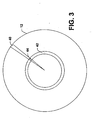
- a servo wedge 40 is read from a track 42 that generally includes track identification information and track misregistration information 44.
- the track misregistration information may also be referred to as position error information.
- the position error information 44 may be provided as servo bursts and may be used during both read and write operations to ensure that the read/write heads are properly aligned on a track.
- the servo controller As a result of receiving the position error information, the servo controller generates a corresponding control signal to position the read/write heads 20 via the voice coil motor.
- the track identification information 44 from the servo wedge 40 is also used during read and write operations so that a track 42 may be properly identified.
- the density of the data stored on each side of each platter must be increased. This places significant burdens on the hard disk drive electronic circuitry. For example, as the density increases, the magnetic transitions that are used to store data on the platters must be physically located more closely together. This often results in intersymbol interference when performing a read operation. As a result, the hard disk drive electronic circuitry must provide more sophisticated processing circuitry that operates at higher frequencies to accurately process the intersymbol interference and the higher frequency read signal. In some cases, the spindle motor speed is increased which further increases the frequency of the read signal and the write signal. Furthermore, the increase in density requires that the servo control system be provided with a higher bandwidth to increase the read/write head positioning resolution.
- the spindle motor speed is being increased from a platter rotational speed of about 5400 RPMs to about 7200 RPMs or greater.
- the write-to-read transition timing for a head 20 becomes important. For example, when performing a write operation, the head 20 is traversing a track 42 on the platter 12 as the platter spins there beneath. As illustrated in Fig. 3, when a servo region or wedge 40 is encountered, the head 20 must quickly transition from a write state to a read state in order to read the servo information stored therein and then quickly transition back to a write state in order to continue writing the data to the platter 12.
- the servo wedge 40 must be larger since the platter is rotating at a generally constant speed. Since many servo wedges 40 exist on the platter 12 ( e.g. , about 60) an optimized write-to-read transition timing allows for the wedges 40 to be minimized, thereby increasing data storage density thereon.
- the present invention relates to a system and method for reducing a write-to-read switching time in a hard disk drive preamplifier circuit.
- the write-to-read switching time is reduced from conventional preamplifier circuits by incorporating a concurrent application of DC bias voltages to all stages of the preamplifier circuit while instituting a staggered squelch deactivation mechanism to prevent saturation of the preamplifier circuit.
- a staggered squelch deactivation mechanism allows for the concurrent application of DC bias voltages by preventing glitches that may be generated by the DC bias voltages from saturating the amplifier circuit.
- the present invention also may include a pole shifting component in the preamplifier circuit that is operable to prevent low frequency glitches that may occur due to the staggered squelch deactivation mechanism from saturating the preamplifier circuit.
- the pole shifting component is selectively employable or programmable such that upon activation, a pole is shifted for a predetermined period of time, at which point a cutoff frequency associated with a high pass filter is increased to ensure rejection of any such glitches through the preamplifier circuit. After the predetermined time, the pole is shifted back to its original position, thereby reducing the cutoff frequency of the high pass filter to permit reading of data at lower frequencies in an expeditious manner.
- a preamplifier circuit comprises a plurality of amplifier stages which are operable to consecutively amplify a signal detected by a head of a hard disk drive.
- the preamplifier circuit further comprises a power delivery circuit which is operably coupled to the amplifier stages and operable to provide power to each of the amplifier stages in a substantially concurrent manner, thereby reducing a settling time associated therewith.
- a control circuit is operably coupled to the amplifier stages and is operable to activate the amplifier stages by deactivating a squelch mechanism associated therewith in a staggered manner, thereby eliminating or otherwise mitigating glitches associated with the substantially concurrent application of power to the amplifier stages from saturating the preamplifier circuit.
- the preamplifier circuit comprises a pole shifting circuit operably coupled to one of the amplifier stages which is operable to interface with such amplifier stage to form a programmable high pass filter circuit.
- the high pass filter may be programmable to the extent that when a read state is detected, for example, the cutoff frequency associated therewith is increased to reject low frequency noise which may be generated by the concurrent DC bias application and/or the staggered squelch deactivation and thus prevent saturation of the preamplifier circuit.
- the cutoff frequency is decreased by shifting a pole associated therewith to about its original position to allow for passing of data therethrough which may exist at lower signal frequencies.
- a preamplifier circuit comprises a plurality of differential amplifier stages coupled together in series.
- the preamplifier circuit comprises a DC bias delivery circuit which is operable to delivery positive and negative DC bias voltages to each of the amplifier stages at about the same time when a read mode is detected. Application of such DC bias voltages to each of the amplifier stages at about the same time reduces an aggregate settling time for all of the amplifier stages and thus permits reading data more quickly than conventional solutions.
- the preamplifier circuit comprises a squelch circuit which is operable to short out the differential input or output of multiple amplifier stages in a staggered manner according to a predetermined timing after the read mode is detected.
- a programmable high pass filter circuit operates in conjunction with the above DC bias delivery circuit and the squelch circuit to prevent low frequency noise or glitches associated therewith from adversely impacting a write-to-read switching time.
- the programmable high pass filter is operable to shift a pole upon a detection of a read mode to increase a cutoff frequency associated therewith. Consequently, any low frequency glitches or excursions that may be generated by the squelch circuit is rejected in the preamplifier circuit during write-to-read switching. After a predetermined period of time, the cutoff frequency is reduced by shifting back the pole to about its original position to allow for low frequency data which is read by the head to pass therethrough.
- a method of reducing a write-to-read switching time in a hard disk drive preamplifier circuit comprises detecting an initiation of a read mode and coupling DC bias voltages to a plurality of amplifier stages in the preamplifier circuit at about the same time. Consequently, an aggregate settling time associated with the powering up of the amplifier stages is reduced.
- the method comprises selectively activating the amplifier stages in a predetermined order by deactivating one or more squelch conditions associated therewith in a staggered fashion upon detection of the detected read state. Such selective activation prevents glitches associated with the application of the DC bias voltages from saturating the preamplifier circuit.
- the method of reducing the write-to-read switching time further comprises increasing a cutoff frequency of a high pass filter associated with the amplifier stages upon detecting the read state to thereby reject low frequency glitches or noise caused by the DC bias voltages or the selective activation of the amplifier stages in a predetermined order. After a predetermined period of time, the cutoff frequency is reduced back to an original value to thereby allow low frequency data signals to pass therethrough.
- the present invention is directed to a system and method of reducing a write-to-read switching time in a hard disk drive system.
- a write-to-read switching time is provided below.
- a read portion of the preamplifier circuit is powered down to reduce power consumption and to prevent spurious noise, etc. from passing through to an output of the read portion of the preamplifier circuit.
- the hard disk drive system switches from a write operation to a read operation, the read portion of the preamplifier circuit must be powered up in order to initiate a read operation. The powering up of the read portion of the preamplifier circuit requires a settling of various circuits therein.
- the time it takes for the preamplifier circuit to settle within 10 mV of its final settling value is typically defined as the preamplifier's write-to-read switching time. As is evident from the discussion above, it is desirable to minimize the write-to-read switching time in order to maximize utilization of the disk drive.
- the inventors of the present invention appreciated that several aspects of conventional preamplifier circuits negatively contribute to an undesirably long write-to-read switching time.
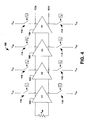
- a conventional preamplifier circuit will be discussed briefly in conjunction with Fig. 4, which is designated at reference numeral 100.
- the preamplifier circuit 100 comprises a plurality of differential amplifier stages 102, 104, 106 and 108 coupled together in series.
- the first amplifier 102 is a high gain stage amplifier which detects a differential signal across the head (depicted as load resistance R MR ) and outputs an amplified signal associated therewith at its output.
- the second amplifier stage 104 typically multiplexes several read channels together, such that signals from multiple heads driving multiple first stages 102 are multiplexed into a single second stage 104 and amplified on its output.
- the third and fourth amplifier stages 106 and 108 typically are low gain stages and perform various functions such as gain control.
- the multiple stages 102, 104, 106 and 108 are not powered up in order to reduce power consumption. That is, the DC bias voltages such as V DD and V SS are not applied to the various stages, for example, by disconnecting such DC bias voltages via switches 110 as illustrated in Fig. 4.
- a control circuit (not shown) powers up the amplifier stages 102, 104, 106 and 108 by closing the switches 110 via a plurality of control signals.
- the control circuit In order to avoid glitches associated with the DC bias voltages from saturating the preamplifier circuit 100, however, the control circuit first closes switches associated with the first amplifier stage 102 ( e.g., at time t 1 ) and then waits for the high gain amplifier stage 102 to settle before closing the switches for the other stages ( e.g., at a later time t 2 ). Such consecutive activation of the amplifier stages is to prevent glitches which may be generated in the stage by the coupling of the DC bias voltage from propagating and getting amplified through the various stages and saturating the preamplifier circuit.
- conventional preamplifier circuit such as the circuit 100 apply the DC bias voltages to the amplifier stages in two or more discrete time periods such that the aggregate settling time for the entire preamplifier circuit 100 is based on a combination of the settling times of the first stage 102 and the other stages 104, 106 and 108. It was appreciated by the inventors of the present invention that such an aggregate settling time adversely impacts the write-to-read switching time of the preamplifier circuit.
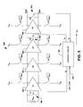
- a preamplifier circuit according to one exemplary aspect of the present invention is illustrated in Fig. 5, and designated at reference numeral 150.
- the preamplifier circuit 150 comprises the plurality of differential amplifier stages 102, 104, 106 and 108 coupled together in series in a manner similar to Fig. 4.
- the preamplifier circuit 150 also has DC bias voltages V DD and V SS which are selectively coupled to the amplifier stages via the switches 110.
- the preamplifier circuit 150 differs from the conventional preamplifier circuit 100 of Fig. 4 in that the DC bias voltages are delivered to the amplifier stages in a substantially concurrent manner. That is, upon detection of a read mode condition, the DC bias voltages are coupled to each of the multiple amplifier stages at about the same time, for example, substantially simultaneously.
- the preamplifier circuit 150 includes a power delivery circuit such as a control circuit 152 which is operable to detect an initiation of a read mode via a signal 154 and generate a plurality of control signals to activate each of the switches 110 at about the same time ( e.g., t all ).
- a power delivery circuit such as a control circuit 152 which is operable to detect an initiation of a read mode via a signal 154 and generate a plurality of control signals to activate each of the switches 110 at about the same time ( e.g., t all ).
- the preamplifier circuit 150 of Fig. 5 further includes a squelch circuit illustrated collectively by reference numeral 160.
- the squelch circuit 160 is operable to activate several of the amplifier stages in a predetermined order upon the detection of the read mode via, for example, the control circuit 152.
- the squelch circuit 160 comprises a plurality of switches S1, S2 and S3 coupled across a differential input or output of various ones of the amplifier stages. When closed in a write mode, the switches S1, S2 and S3 short out amplifier stages 102 and 108 and prevent any spurious noise or glitches from the head R MR from passing therethrough to the output thereof (illustrated, for example, as differential output RDX and RDY).
- the squelch circuit 160 When the read mode is detected by the control circuit 152, the squelch circuit 160 is operable to activate the multiple amplifier stages by opening the switches S1, S2 and S3 in a predetermined order. For example, after waiting a predetermined time period (e.g., t D1 ), the control circuit 152 opens switch S1, thus activating the first amplifier stage 102. Then, after awaiting another predetermined time after the read mode is detected (e.g., t D2 ), the control circuit 152 opens switch S2, and after time period t D3 , S3 is opened. Therefore the squelch circuit 160 and the control circuit 152 operate to open the switches S1, S2 and S3 in a staggered fashion.
- a predetermined time period e.g., t D1
- the control circuit 152 opens switch S1, thus activating the first amplifier stage 102. Then, after awaiting another predetermined time after the read mode is detected (e.g., t D2 ), the control circuit 152
- the squelch circuit 160 operates to prevent glitches associated with the substantially concurrent application of DC bias voltages to the amplifier stages. For example, when V DD and V SS are applied to the amplifier stages 102, 104, 106 and 108, glitches are generated therein. Since S1 is closed, however, indicating a squelch condition, no glitch forms on the output of the first amplifier stage 102. Likewise, any glitches generated in amplifier stages 104 and 106 due to the DC bias voltages are squelched by S2 which is closed when the DC bias voltages are provided. Lastly, any glitch generated in the last amplifier stage 108 is squelched by the closed switch S3. Therefore the squelch circuit 160 operates to prevent saturation of the preamplifier circuit 150 when the DC bias voltages are provided to the amplifier stages in a substantially concurrent manner, thus enabling a faster settling time and reducing the write-to-read switching time.
- any glitches associated with the application of the DC bias voltages are squelched.
- S1 is opened by the control circuit 152.
- the opening of S1 itself causes a glitch at the output of the amplifier stage 102 that propagates through stages 104 and 106, however, since S2 is still closed, the glitch gets squelched, thus preventing saturation of the preamplifier circuit 150.
- S2 opens which itself causes a glitch in the last amplifier stage 108.
- the squelch circuit 160 prevents saturation of the preamplifier circuit 150 due to the DC bias voltage application in a substantially concurrent manner.
- the staggered deactivation of the switches S1, S2 and S3 further protects the saturation of the preamplifier circuit.
- the write-to-read switching time is decreased, and any glitches associated therewith are squelched by the squelch circuit, thereby preventing an undesirable saturation of the preamplifier circuit 150.
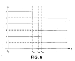
- the staggered activation or opening of switches S1, S2 and S3 are performed in the following manner, as illustrated in Fig. 6.
- the control circuit 152 waits a time period t D1 (e.g., about 55 ns) which is a time period expected to be long enough to ensure that any glitches associated with the coupling of the DC bias voltages to each of the amplifier stages at about the same time are squelched, thus preventing preamplifier saturation.
- t D1 e.g., about 55 ns
- S1 opens which causes a glitch to propagate through amplifier stages 102, 104 and 106.
- the squelch circuit 160 in connection with delivery of the DC bias voltages in a substantially concurrent manner decreases the write-to-read switching time in the preamplifier circuit over conventional solutions. Even with the squelch circuit 160, however, some excursions may still occur during the write-to-read mode transition. For example, when S1 opens, a low frequency, relatively long duration glitch (e.g. , having a time constant of about 150 ns, a frequency of about 1-2 MHz) may occur that may propagate through amplifier stages 104, 106 and 108 despite the squelching operations. Therefore according to another aspect of the present invention, a programmable or otherwise selectively employable high pass filter circuit is incorporated into the preamplifier circuit of Fig. 5, for example, by supplementing circuitry associated with the third amplifier stage 106. The present invention contemplates use of a programmable high pass filtering circuit which varies the cutoff frequency thereof based on a detection of a write to read mode transition.
- a programmable high pass filtering circuit which
- the programmable high pass filter circuit may operate as a pole shifting circuit which is activated to shift a pole associated therewith when a read mode is detected, thereby increasing a cutoff frequency (e.g., from about 1-2 MHz to about 10 MHz) associated therewith for a predetermined period of time.
- a cutoff frequency e.g., from about 1-2 MHz to about 10 MHz
- the pole After the predetermined period of time (e.g., t DELAY of about 90 ns), the pole is shifted back to about its original position, thereby decreasing the cutoff frequency associated therewith (e.g., back to about 1-2 MHz) to allow low frequency data to be read during the read mode.
- t DELAY a predetermined period of time
- the high pass filter circuit 190 comprises another amplifier stage 192 coupled in parallel with the third amplifier stage 106, wherein the amplifier stages 106 and 192 have the same gain associated therewith.
- the differential output of the amplifier stage 192 is fed into a low pass filter circuit (LPF) 194 having a programmable cutoff frequency control signal 196 associated therewith.
- the control signal 196 is operable to provide a digital type signal, wherein one state dictates a first cutoff frequency and the second state dictates a second cutoff frequency, respectively.
- the output of the low pass filter circuit 194 results in a signal in which all signal frequency components which exceed the cutoff frequency are rejected.
- the output of the low pass filter circuit 194 is then fed to a subtraction circuit 198 in which the output of low pass filter circuit 194 is subtracted from the output of the third amplifier stage 106.
- the output of the subtraction circuit thus results in a signal in which all signal frequency components below the cutoff frequency of the LPF 194 are rejected, thereby operating macroscopically as a high pass filter.
- the high pass filter circuit 190 has a programmable cutoff frequency which is controlled by the cutoff frequency control signal 196 from, for example, the control circuit 152.
- the cutoff frequency of the low pass filter circuit 194 is set at a first, lower frequency (e.g. , about 1-2 MHz).
- the control signal 196 changes state when the read mode is detected and the low pass filter circuit 194 is operable to adjust its cutoff frequency to a second, higher frequency (e.g., about 10 MHz).
- the high pass filter circuit 190 is operable to reject any noise or low frequency excursions which fall below the second cutoff frequency which is now a larger range of frequencies.
- the control signal 196 again changes state, thereby lowering the cutoff frequency of the low pass filter circuit 194 back to its original cutoff frequency for the remainder of the read mode. With the lower cutoff frequency re-established, the high pass filter circuit 190 will pass lower frequency signals in the 2 MHz range which may comprise data read by the head.
- the circuit 250 includes an input 252 in which the output of the amplifier stage 106 is fed into a delay block 254 and a low pass filter circuit 256.
- the delay block 254 is advantageously employed to synchronize the subsequent subtraction of the input 254 from a filtered version of the input at the decision block 258.
- the low pass filter 256 is operable to pass signals having a frequency below a cutoff frequency, the cutoff frequency f LPF being a function of the desired pole.
- Fig. 8b illustrates an exemplary low pass response for the low pass filter 194 in a read state, wherein signals having frequencies above the cutoff frequency f LPF are rejected.
- a first graph 310 represents a frequency range associated with an input signal to the low pass filter 194 and a second graph 312 represents a frequency range associated with the output of the low pass filter 194.
- a high pass response 314 By subtracting the low pass response 312 from that of response 310, a high pass response 314, as illustrated in Fig. 8b, wherein the low frequency cutoff f LPF is a function of the cutoff frequency of the low pass filter. Therefore by varying the cutoff frequency of the low pass filter 194, the pole of the circuit may be moved from a first frequency to a second frequency when the preamplifier is transitioning from a non-read state such as the write state to the read state.
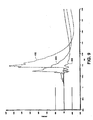
- Fig. 9 illustrates the write-to-read switching times of three different preamplifier circuit.
- One voltage waveform 402 is associated with the conventional preamplifier circuit 100 of Fig. 4. Note that such a preamplifier circuit 100 consecutively applies the DC bias voltages upon detection of a read mode at about the 1 microsecond time period.
- the waveform 402 ultimately is within about 10 mV of its final intended settling time value of 0V within about 350 nS which is about the write-to-read switching time of the conventional preamplifier circuit 100.
- a second waveform 404 illustrates the preamplifier circuit 150 of Fig. 5 which applies the DC bias voltages to each of the amplifier stages at about the same time, and incorporates a squelch circuit to mitigate glitches associated therewith.
- the waveform 404 indicates a shorter aggregate settling time for the amplifier stages to be operational (as indicated by the earlier initial spike than the waveform 402).
- the waveform 404 show a relatively low frequency glitch propagating therethrough, thus resulting in a write-to-read switching time of about 200 nS, which still represents a significant improvement over the preamplifier circuit 100.
- Fig. 9 illustrates a third waveform 406 that incorporates the preamplifier circuit 150 with the programmable high pass filter circuit 190 of Fig. 7. Note that in the waveform 406, the low frequency glitch of waveform 404 has been filtered out. Therefore the signal of waveform 406 does not extend outside the 10 mV guardband used to measure the write-to-read switching time. However, because the programmable period in which the cutoff frequency is increased to about 10 MHz is about 90 nS, and since it takes about another 10 nS to move the cutoff frequency back to about 1-2 MHz, the minimum time at which data reading may commence is about 100 nS. Therefore a combination of the various aspects of the present invention allow for a reduction in the write-to-read switching time of the preamplifier from about 350 nS to about 100 nS.
- a method of reducing a write-to-read switching time is disclosed, as illustrated in Fig. 10. While, for purposes of simplicity of explanation, the methodology of Fig. 10 is shown and described as a series of steps, it is to be understood and appreciated that the present invention is not limited to the order of steps, as some steps may, in accordance with the present invention, occur in different orders and/or concurrently with other steps from that shown and described herein. For example, a methodology in accordance with an aspect of the present invention may be represented as a combination of various states ( e.g. , in a state diagram). Moreover, not all illustrated steps may be required to implement a methodology in accordance with an aspect the present invention.
- the methodology begins at step 502, wherein an initiation of a read mode is detected.
- detection may be accomplished by monitoring a status of a binary signal or a value of a digital word which represents a status of the hard disk drive. Any manner, however, of detecting a read mode condition may be utilized and is contemplated as falling within the scope of the present invention.
- the DC bias voltages used to power each of the amplifier stages are coupled thereto in a substantially concurrent manner. That is, the DC bias voltages are not coupled to selective ones of the amplifier stages and then subsequently applied to other stages after a predetermined wait time in order to allow for settling of the first powered stages as done conventionally.
- the aggregate settling time for all of the stages to be powered up and ready to operate is reduced substantially.
- the method 500 continues at step 506, wherein selective portions of a squelch circuit are deactivated in a staggered fashion. For example, prior to a read state being detected, the portions of the squelch circuit are activated, thereby squelching one or more of the amplifier stages to prevent spurious noise, etc. from passing through the read preamplifier when not in a read mode.
- the squelch circuit begins its selective deactivation mode in order to prevent glitches incurred from the concurrent application of the DC bias voltages from saturating the preamplifier.
- step 506 comprises maintaining the squelch conditions on the amplifier stages for a predetermined period of time (e.g. , about 55 nS) to ensure the DC bias voltage glitches are squelched effectively. Then a squelch condition on a first amplifier stage (e.g., stage 102) is deactivated while other squelch conditions are maintained, thus preventing glitches therefrom from saturating the preamplifier circuit. Then, after more time (e.g., another 10 nS) another squelch condition associated with the preamplifier circuit output is deactivated.
- the staggered deactivation of the squelch conditions prevents DC bias glitches from saturating the preamplifier and also prevents glitches associated with the squelch deactivation process itself from saturating the preamplifier.
- the cutoff frequency of a high pass filter circuit is increased at step 508 for a predetermined period of time. Therefore any low frequency noise or excursions caused by the squelch deactivation process are rejected. After a predetermined period of time (e.g., about 90 nS), the cutoff frequency of the high pass filter is returned to its original state to permit reading of low frequency data.
- a predetermined period of time e.g., about 90 nS
Landscapes
- Digital Magnetic Recording (AREA)
Applications Claiming Priority (2)
| Application Number | Priority Date | Filing Date | Title |
|---|---|---|---|
| US09/709,699 US6621649B1 (en) | 2000-11-10 | 2000-11-10 | Write-to-read switching improvement for differential preamplifier circuits in hard disk drive systems |
| US709699 | 2000-11-10 |
Publications (3)
| Publication Number | Publication Date |
|---|---|
| EP1205928A2 true EP1205928A2 (de) | 2002-05-15 |
| EP1205928A3 EP1205928A3 (de) | 2007-08-08 |
| EP1205928B1 EP1205928B1 (de) | 2010-05-12 |
Family
ID=24850979
Family Applications (1)
| Application Number | Title | Priority Date | Filing Date |
|---|---|---|---|
| EP01000616A Expired - Lifetime EP1205928B1 (de) | 2000-11-10 | 2001-11-09 | Verbesserung bei der Umschaltung von Schreiben auf Lesen für differentielle Vorverstärkerschaltungen in Festplattenantriebsystemen |
Country Status (7)
| Country | Link |
|---|---|
| US (1) | US6621649B1 (de) |
| EP (1) | EP1205928B1 (de) |
| JP (1) | JP4027644B2 (de) |
| KR (1) | KR100846002B1 (de) |
| AT (1) | ATE467892T1 (de) |
| DE (1) | DE60142104D1 (de) |
| TW (1) | TW577053B (de) |
Cited By (1)
| Publication number | Priority date | Publication date | Assignee | Title |
|---|---|---|---|---|
| EP1587099A2 (de) * | 2004-04-17 | 2005-10-19 | Agere Systems, Inc. | Verringerte Erholungsszeit für senkrechte Aufzeichnung |
Families Citing this family (15)
| Publication number | Priority date | Publication date | Assignee | Title |
|---|---|---|---|---|
| GB2368712A (en) * | 2000-10-31 | 2002-05-08 | Hewlett Packard Co | Data reader |
| SG115437A1 (en) * | 2000-12-27 | 2005-10-28 | Toshiba Kk | Disk drive including preamplifier for perpendicular magnetic recording system |
| JP2002304701A (ja) * | 2001-04-10 | 2002-10-18 | Sony Corp | 再生アンプおよびこれを用いた磁気記録再生装置 |
| US6847500B2 (en) * | 2001-09-06 | 2005-01-25 | Hitachi Global Storage Technologies Netherlands B.V. | Methods and apparatus for gradually decreasing supply current demand in arm electronics for write-to-read transitions |
| US6954321B2 (en) * | 2002-02-21 | 2005-10-11 | Hitachi Global Storage Technologies, Netherlands B.V. | Method and apparatus for improved read-to-write transition time for a magneto-resistive head |
| US6831584B2 (en) * | 2002-09-03 | 2004-12-14 | Broadcom Corporation | High-speed low-distortion analog-to digital converter |
| JP2004127409A (ja) * | 2002-10-01 | 2004-04-22 | Toshiba Corp | ディスク記憶装置及びデータ再生方法 |
| US7339760B2 (en) * | 2004-01-30 | 2008-03-04 | Agere Systems Inc. | Integrated bias and offset recovery amplifier |
| US7199981B2 (en) | 2004-03-19 | 2007-04-03 | Zabtcioglu Fikret M | High reliability-parallel data transfer hard disk drive |
| US7317586B1 (en) * | 2004-06-07 | 2008-01-08 | Maxtor Corporation | Methods and structure for general purpose interval accumulating filter for measuring operational parameters of a digital read channel |
| US7600136B2 (en) * | 2005-08-19 | 2009-10-06 | Seagate Technology Llc | Power management in an information channel |
| US7619841B1 (en) | 2005-11-23 | 2009-11-17 | Western Digital Technologies, Inc. | Disk drive subtracting low frequency disturbance from a servo burst signal |
| JP2007149274A (ja) * | 2005-11-30 | 2007-06-14 | Hitachi Ltd | 再生回路及びそれを用いた磁気ディスク装置 |
| JP4957734B2 (ja) * | 2009-02-10 | 2012-06-20 | ソニー株式会社 | 受信装置、撮像装置及び受信方法 |
| US9099156B2 (en) * | 2013-10-08 | 2015-08-04 | Marvell World Trade Ltd. | Two-dimensional magnetic recording systems and methods for minimizing and accounting for inter-modulation of signals induced in adjacent read elements |
Citations (2)
| Publication number | Priority date | Publication date | Assignee | Title |
|---|---|---|---|---|
| US5648738A (en) | 1994-11-01 | 1997-07-15 | Cirrus Logic, Inc. | Read channel having auto-zeroing and offset compensation, and power-down between servo fields |
| US5959798A (en) | 1992-10-30 | 1999-09-28 | Sony Corporation | Reproducing circuit for a magnetic head having a variable gain amplifier with selective adjustment of the gain during recording and reproduction |
Family Cites Families (14)
| Publication number | Priority date | Publication date | Assignee | Title |
|---|---|---|---|---|
| JPH0439863U (de) * | 1990-07-25 | 1992-04-03 | ||
| JPH05327690A (ja) * | 1992-05-21 | 1993-12-10 | Hitachi Ltd | 通信方法および装置 |
| JP3233472B2 (ja) * | 1993-01-07 | 2001-11-26 | 株式会社東芝 | データ通信装置 |
| JP2559966B2 (ja) * | 1993-03-08 | 1996-12-04 | インターナショナル・ビジネス・マシーンズ・コーポレイション | 磁気記録装置の読取り/書込み回路 |
| US6172548B1 (en) * | 1994-12-30 | 2001-01-09 | Stmicroelectronics, Inc. | Input stage with reduced transient time for use in multiplexing transducers that require a switched DC bias |
| US5781042A (en) * | 1995-09-19 | 1998-07-14 | Vtc Inc. | Modal transition imbalance detector |
| US6112324A (en) | 1996-02-02 | 2000-08-29 | The Arizona Board Of Regents Acting On Behalf Of The University Of Arizona | Direct access compact disc, writing and reading method and device for same |
| US5822142A (en) | 1996-07-26 | 1998-10-13 | Western Digital Corporation | Method of mapping logical sectors to physical sectors in a disk drive sparing partition |
| US6028727A (en) | 1997-09-05 | 2000-02-22 | Cirrus Logic, Inc. | Method and system to improve single synthesizer setting times for small frequency steps in read channel circuits |
| US6141169A (en) * | 1997-10-23 | 2000-10-31 | Cirrus Logic, Inc. | System and method for control of low frequency input levels to an amplifier and compensation of input offsets of the amplifier |
| US6111712A (en) | 1998-03-06 | 2000-08-29 | Cirrus Logic, Inc. | Method to improve the jitter of high frequency phase locked loops used in read channels |
| US6219194B1 (en) * | 1999-04-09 | 2001-04-17 | Guzik Technical Enterprises | MR head read amplifier with improved write to read recovery time |
| US6473253B1 (en) * | 1999-04-28 | 2002-10-29 | Koninklijke Philips Electronics N.V. | Read channel with programmable bandwidth control |
| US6424480B1 (en) * | 1999-09-28 | 2002-07-23 | Koninklijke Philips Electronics N.V. | Magnetic medium storage apparatus with read channel having a programmable write-to-read suppression |
-
2000
- 2000-11-10 US US09/709,699 patent/US6621649B1/en not_active Expired - Lifetime
-
2001
- 2001-11-09 TW TW090127875A patent/TW577053B/zh not_active IP Right Cessation
- 2001-11-09 DE DE60142104T patent/DE60142104D1/de not_active Expired - Lifetime
- 2001-11-09 EP EP01000616A patent/EP1205928B1/de not_active Expired - Lifetime
- 2001-11-09 AT AT01000616T patent/ATE467892T1/de not_active IP Right Cessation
- 2001-11-10 KR KR1020010069963A patent/KR100846002B1/ko active IP Right Grant
- 2001-11-12 JP JP2001346430A patent/JP4027644B2/ja not_active Expired - Fee Related
Patent Citations (2)
| Publication number | Priority date | Publication date | Assignee | Title |
|---|---|---|---|---|
| US5959798A (en) | 1992-10-30 | 1999-09-28 | Sony Corporation | Reproducing circuit for a magnetic head having a variable gain amplifier with selective adjustment of the gain during recording and reproduction |
| US5648738A (en) | 1994-11-01 | 1997-07-15 | Cirrus Logic, Inc. | Read channel having auto-zeroing and offset compensation, and power-down between servo fields |
Cited By (3)
| Publication number | Priority date | Publication date | Assignee | Title |
|---|---|---|---|---|
| EP1587099A2 (de) * | 2004-04-17 | 2005-10-19 | Agere Systems, Inc. | Verringerte Erholungsszeit für senkrechte Aufzeichnung |
| EP1587099A3 (de) * | 2004-04-17 | 2005-12-28 | Agere Systems, Inc. | Verringerte Erholungsszeit für senkrechte Aufzeichnung |
| US7119977B2 (en) | 2004-04-17 | 2006-10-10 | Agere Systems Inc. | Reduced recovery time for perpendicular recording systems |
Also Published As
| Publication number | Publication date |
|---|---|
| EP1205928B1 (de) | 2010-05-12 |
| KR100846002B1 (ko) | 2008-07-11 |
| EP1205928A3 (de) | 2007-08-08 |
| DE60142104D1 (de) | 2010-06-24 |
| JP2002197601A (ja) | 2002-07-12 |
| US6621649B1 (en) | 2003-09-16 |
| JP4027644B2 (ja) | 2007-12-26 |
| ATE467892T1 (de) | 2010-05-15 |
| TW577053B (en) | 2004-02-21 |
| KR20020036769A (ko) | 2002-05-16 |
Similar Documents
| Publication | Publication Date | Title |
|---|---|---|
| US6621649B1 (en) | Write-to-read switching improvement for differential preamplifier circuits in hard disk drive systems | |
| US8854752B2 (en) | Systems and methods for track width determination | |
| EP1160788B1 (de) | Plattengerät und Plattenmedium | |
| US8134792B2 (en) | Preamplifier and method for synchronization with bit patterned media | |
| US7142380B2 (en) | Magnetic recording/reproducing apparatus and magnetic recording/reproducing method | |
| US7821734B2 (en) | Head IC, read circuit and medium storage device | |
| US7605993B2 (en) | Write current boosted head amplifier | |
| US6963459B2 (en) | Method and apparatus for optimizing auto gain control of read channel in a disk drive | |
| US5982569A (en) | Read/write data interface and method of operation | |
| US6587296B1 (en) | Capacitor bias recovery methodology | |
| EP1174874B1 (de) | Vorverstärker-Leserückgewinnungsparade | |
| US6785083B2 (en) | Application of reduced bias levels to disc drive read elements during periods of inactivity | |
| US20050094303A1 (en) | Flying height monitor with servo AGC voltage for write operation in a hard disk drive | |
| US20190392862A1 (en) | Microwave-assisted magnetic recording apparatus and method | |
| US6222691B1 (en) | Interleaved dibit detection for direct access storage device (DASD) | |
| JP2002092803A (ja) | 磁気ディスク装置 | |
| US6819516B2 (en) | WUS (unsafe) detection (kick back sensing) | |
| US20020122265A1 (en) | CMOS DC offset correction circuit with programmable high-pass transfer function | |
| US6819515B1 (en) | Method and circuit for eliminating glitches in a disk drive read head | |
| JP3866487B2 (ja) | ディスク装置 | |
| US20080007869A1 (en) | Disk drive and magnetic storage medium | |
| US8134805B2 (en) | Silent retract of heads in a hard disk drive | |
| US20020075054A1 (en) | Read gain offset trim without feedback loop | |
| JP2004342239A (ja) | 回転磁気ヘッド型記録再生装置 |
Legal Events
| Date | Code | Title | Description |
|---|---|---|---|
| PUAI | Public reference made under article 153(3) epc to a published international application that has entered the european phase |
Free format text: ORIGINAL CODE: 0009012 |
|
| AK | Designated contracting states |
Kind code of ref document: A2 Designated state(s): AT BE CH CY DE DK ES FI FR GB GR IE IT LI LU MC NL PT SE TR |
|
| AX | Request for extension of the european patent |
Free format text: AL;LT;LV;MK;RO;SI |
|
| RIN1 | Information on inventor provided before grant (corrected) |
Inventor name: JIANG, HONG Inventor name: RANMUTHU, INDUMINI |
|
| PUAL | Search report despatched |
Free format text: ORIGINAL CODE: 0009013 |
|
| AK | Designated contracting states |
Kind code of ref document: A3 Designated state(s): AT BE CH CY DE DK ES FI FR GB GR IE IT LI LU MC NL PT SE TR |
|
| AX | Request for extension of the european patent |
Extension state: AL LT LV MK RO SI |
|
| 17P | Request for examination filed |
Effective date: 20080208 |
|
| AKX | Designation fees paid |
Designated state(s): AT BE CH CY DE DK ES FI FR GB GR IE IT LI LU MC NL PT SE TR |
|
| 17Q | First examination report despatched |
Effective date: 20080618 |
|
| GRAP | Despatch of communication of intention to grant a patent |
Free format text: ORIGINAL CODE: EPIDOSNIGR1 |
|
| GRAS | Grant fee paid |
Free format text: ORIGINAL CODE: EPIDOSNIGR3 |
|
| GRAA | (expected) grant |
Free format text: ORIGINAL CODE: 0009210 |
|
| AK | Designated contracting states |
Kind code of ref document: B1 Designated state(s): AT BE CH CY DE DK ES FI FR GB GR IE IT LI LU MC NL PT SE TR |
|
| REG | Reference to a national code |
Ref country code: GB Ref legal event code: FG4D |
|
| REG | Reference to a national code |
Ref country code: CH Ref legal event code: EP |
|
| REG | Reference to a national code |
Ref country code: IE Ref legal event code: FG4D |
|
| REF | Corresponds to: |
Ref document number: 60142104 Country of ref document: DE Date of ref document: 20100624 Kind code of ref document: P |
|
| REG | Reference to a national code |
Ref country code: NL Ref legal event code: T3 |
|
| PG25 | Lapsed in a contracting state [announced via postgrant information from national office to epo] |
Ref country code: ES Free format text: LAPSE BECAUSE OF FAILURE TO SUBMIT A TRANSLATION OF THE DESCRIPTION OR TO PAY THE FEE WITHIN THE PRESCRIBED TIME-LIMIT Effective date: 20100823 Ref country code: SE Free format text: LAPSE BECAUSE OF FAILURE TO SUBMIT A TRANSLATION OF THE DESCRIPTION OR TO PAY THE FEE WITHIN THE PRESCRIBED TIME-LIMIT Effective date: 20100512 |
|
| PG25 | Lapsed in a contracting state [announced via postgrant information from national office to epo] |
Ref country code: FI Free format text: LAPSE BECAUSE OF FAILURE TO SUBMIT A TRANSLATION OF THE DESCRIPTION OR TO PAY THE FEE WITHIN THE PRESCRIBED TIME-LIMIT Effective date: 20100512 Ref country code: AT Free format text: LAPSE BECAUSE OF FAILURE TO SUBMIT A TRANSLATION OF THE DESCRIPTION OR TO PAY THE FEE WITHIN THE PRESCRIBED TIME-LIMIT Effective date: 20100512 |
|
| PG25 | Lapsed in a contracting state [announced via postgrant information from national office to epo] |
Ref country code: GR Free format text: LAPSE BECAUSE OF FAILURE TO SUBMIT A TRANSLATION OF THE DESCRIPTION OR TO PAY THE FEE WITHIN THE PRESCRIBED TIME-LIMIT Effective date: 20100813 Ref country code: CY Free format text: LAPSE BECAUSE OF FAILURE TO SUBMIT A TRANSLATION OF THE DESCRIPTION OR TO PAY THE FEE WITHIN THE PRESCRIBED TIME-LIMIT Effective date: 20100512 |
|
| PG25 | Lapsed in a contracting state [announced via postgrant information from national office to epo] |
Ref country code: DK Free format text: LAPSE BECAUSE OF FAILURE TO SUBMIT A TRANSLATION OF THE DESCRIPTION OR TO PAY THE FEE WITHIN THE PRESCRIBED TIME-LIMIT Effective date: 20100512 Ref country code: PT Free format text: LAPSE BECAUSE OF FAILURE TO SUBMIT A TRANSLATION OF THE DESCRIPTION OR TO PAY THE FEE WITHIN THE PRESCRIBED TIME-LIMIT Effective date: 20100913 |
|
| PG25 | Lapsed in a contracting state [announced via postgrant information from national office to epo] |
Ref country code: BE Free format text: LAPSE BECAUSE OF FAILURE TO SUBMIT A TRANSLATION OF THE DESCRIPTION OR TO PAY THE FEE WITHIN THE PRESCRIBED TIME-LIMIT Effective date: 20100512 |
|
| PLBE | No opposition filed within time limit |
Free format text: ORIGINAL CODE: 0009261 |
|
| STAA | Information on the status of an ep patent application or granted ep patent |
Free format text: STATUS: NO OPPOSITION FILED WITHIN TIME LIMIT |
|
| PG25 | Lapsed in a contracting state [announced via postgrant information from national office to epo] |
Ref country code: IT Free format text: LAPSE BECAUSE OF FAILURE TO SUBMIT A TRANSLATION OF THE DESCRIPTION OR TO PAY THE FEE WITHIN THE PRESCRIBED TIME-LIMIT Effective date: 20100512 |
|
| 26N | No opposition filed |
Effective date: 20110215 |
|
| REG | Reference to a national code |
Ref country code: DE Ref legal event code: R097 Ref document number: 60142104 Country of ref document: DE Effective date: 20110214 |
|
| PG25 | Lapsed in a contracting state [announced via postgrant information from national office to epo] |
Ref country code: MC Free format text: LAPSE BECAUSE OF NON-PAYMENT OF DUE FEES Effective date: 20101130 |
|
| REG | Reference to a national code |
Ref country code: CH Ref legal event code: PL |
|
| PG25 | Lapsed in a contracting state [announced via postgrant information from national office to epo] |
Ref country code: LI Free format text: LAPSE BECAUSE OF NON-PAYMENT OF DUE FEES Effective date: 20101130 Ref country code: CH Free format text: LAPSE BECAUSE OF NON-PAYMENT OF DUE FEES Effective date: 20101130 |
|
| PG25 | Lapsed in a contracting state [announced via postgrant information from national office to epo] |
Ref country code: IE Free format text: LAPSE BECAUSE OF NON-PAYMENT OF DUE FEES Effective date: 20101109 |
|
| PG25 | Lapsed in a contracting state [announced via postgrant information from national office to epo] |
Ref country code: LU Free format text: LAPSE BECAUSE OF NON-PAYMENT OF DUE FEES Effective date: 20101109 |
|
| PG25 | Lapsed in a contracting state [announced via postgrant information from national office to epo] |
Ref country code: TR Free format text: LAPSE BECAUSE OF FAILURE TO SUBMIT A TRANSLATION OF THE DESCRIPTION OR TO PAY THE FEE WITHIN THE PRESCRIBED TIME-LIMIT Effective date: 20100512 |
|
| REG | Reference to a national code |
Ref country code: FR Ref legal event code: PLFP Year of fee payment: 15 |
|
| REG | Reference to a national code |
Ref country code: FR Ref legal event code: PLFP Year of fee payment: 16 |
|
| PGFP | Annual fee paid to national office [announced via postgrant information from national office to epo] |
Ref country code: DE Payment date: 20161130 Year of fee payment: 16 Ref country code: NL Payment date: 20161107 Year of fee payment: 16 Ref country code: GB Payment date: 20161026 Year of fee payment: 16 Ref country code: FR Payment date: 20161017 Year of fee payment: 16 |
|
| REG | Reference to a national code |
Ref country code: DE Ref legal event code: R119 Ref document number: 60142104 Country of ref document: DE |
|
| REG | Reference to a national code |
Ref country code: NL Ref legal event code: MM Effective date: 20171201 |
|
| GBPC | Gb: european patent ceased through non-payment of renewal fee |
Effective date: 20171109 |
|
| REG | Reference to a national code |
Ref country code: FR Ref legal event code: ST Effective date: 20180731 |
|
| PG25 | Lapsed in a contracting state [announced via postgrant information from national office to epo] |
Ref country code: NL Free format text: LAPSE BECAUSE OF NON-PAYMENT OF DUE FEES Effective date: 20171201 Ref country code: FR Free format text: LAPSE BECAUSE OF NON-PAYMENT OF DUE FEES Effective date: 20171130 Ref country code: DE Free format text: LAPSE BECAUSE OF NON-PAYMENT OF DUE FEES Effective date: 20180602 |
|
| PG25 | Lapsed in a contracting state [announced via postgrant information from national office to epo] |
Ref country code: GB Free format text: LAPSE BECAUSE OF NON-PAYMENT OF DUE FEES Effective date: 20171109 |