EP1201899A2 - Steuergerät für einen Kraftfahrzeugmotor - Google Patents
Steuergerät für einen Kraftfahrzeugmotor Download PDFInfo
- Publication number
- EP1201899A2 EP1201899A2 EP01101520A EP01101520A EP1201899A2 EP 1201899 A2 EP1201899 A2 EP 1201899A2 EP 01101520 A EP01101520 A EP 01101520A EP 01101520 A EP01101520 A EP 01101520A EP 1201899 A2 EP1201899 A2 EP 1201899A2
- Authority
- EP
- European Patent Office
- Prior art keywords
- configuration parameters
- control device
- engine
- input
- external computer
- Prior art date
- Legal status (The legal status is an assumption and is not a legal conclusion. Google has not performed a legal analysis and makes no representation as to the accuracy of the status listed.)
- Granted
Links
Images

Classifications
-
- F—MECHANICAL ENGINEERING; LIGHTING; HEATING; WEAPONS; BLASTING
- F02—COMBUSTION ENGINES; HOT-GAS OR COMBUSTION-PRODUCT ENGINE PLANTS
- F02D—CONTROLLING COMBUSTION ENGINES
- F02D41/00—Electrical control of supply of combustible mixture or its constituents
- F02D41/24—Electrical control of supply of combustible mixture or its constituents characterised by the use of digital means
- F02D41/26—Electrical control of supply of combustible mixture or its constituents characterised by the use of digital means using computer, e.g. microprocessor
-
- G—PHYSICS
- G05—CONTROLLING; REGULATING
- G05B—CONTROL OR REGULATING SYSTEMS IN GENERAL; FUNCTIONAL ELEMENTS OF SUCH SYSTEMS; MONITORING OR TESTING ARRANGEMENTS FOR SUCH SYSTEMS OR ELEMENTS
- G05B19/00—Program-control systems
- G05B19/02—Program-control systems electric
- G05B19/04—Program control other than numerical control, i.e. in sequence controllers or logic controllers
- G05B19/042—Program control other than numerical control, i.e. in sequence controllers or logic controllers using digital processors
-
- G—PHYSICS
- G05—CONTROLLING; REGULATING
- G05B—CONTROL OR REGULATING SYSTEMS IN GENERAL; FUNCTIONAL ELEMENTS OF SUCH SYSTEMS; MONITORING OR TESTING ARRANGEMENTS FOR SUCH SYSTEMS OR ELEMENTS
- G05B2219/00—Program-control systems
- G05B2219/20—Pc systems
- G05B2219/23—Pc programming
- G05B2219/23304—Download program from host
-
- G—PHYSICS
- G05—CONTROLLING; REGULATING
- G05B—CONTROL OR REGULATING SYSTEMS IN GENERAL; FUNCTIONAL ELEMENTS OF SUCH SYSTEMS; MONITORING OR TESTING ARRANGEMENTS FOR SUCH SYSTEMS OR ELEMENTS
- G05B2219/00—Program-control systems
- G05B2219/20—Pc systems
- G05B2219/25—Pc structure of the system
- G05B2219/25431—Dual Port memory
-
- G—PHYSICS
- G05—CONTROLLING; REGULATING
- G05B—CONTROL OR REGULATING SYSTEMS IN GENERAL; FUNCTIONAL ELEMENTS OF SUCH SYSTEMS; MONITORING OR TESTING ARRANGEMENTS FOR SUCH SYSTEMS OR ELEMENTS
- G05B2219/00—Program-control systems
- G05B2219/20—Pc systems
- G05B2219/26—Pc applications
- G05B2219/2637—Vehicle, car, auto, wheelchair
-
- G—PHYSICS
- G11—INFORMATION STORAGE
- G11C—STATIC STORES
- G11C16/00—Erasable programmable read-only memories
- G11C16/02—Erasable programmable read-only memories electrically programmable
- G11C16/06—Auxiliary circuits, e.g. for writing into memory
- G11C16/10—Programming or data input circuits
- G11C16/102—External programming circuits, e.g. EPROM programmers; In-circuit programming or reprogramming; EPROM emulators
Definitions
- the present invention relates to a control device for a vehicle engine.
- Engines of modern vehicles have various electronic systems which enable their operation to be controlled in the best possible manner. These systems are controlled by a device which sends corresponding control signals to the engine in accordance with configuration parameters stored in a non-volatile memory of the control device (typically a flash E 2 PROM).
- a non-volatile memory of the control device typically a flash E 2 PROM
- the configuration parameters are corrected to modify the operation of the engine; this calibration operation is typically performed in the factory at the vehicle-development stage, or in the workshop, to adapt the behaviour of the engine to various environmental conditions or conditions of wear of the components.
- the calibration operation is generally performed in the field whilst the engine is in operation in order to check directly the results of the modifications applied.
- the control device is connected to an external computer which controls the modification of the configuration parameters read from the flash memory of the control device.
- the configuration parameters cannot be modified in real time directly in the flash memory of the control device; the writing operation in fact involves the need to cancel the contents of the flash memory at least in blocks and the configuration parameters are therefore not available at the same time for controlling the operation of the engine.
- a known solution consists of the use of a specially constructed (custom) interface card which is connected to the control device by means of a high-speed parallel bus; the external computer is then connected to the interface card by means of a standard connector.
- the configuration parameters can thus be modified directly by the external computer (by means of a standard connection) whilst, at the same time, being used by the control device.
- the new configuration parameters are then downloaded from the RAM memory of the interface card into the flash memory of the control device.
- the object of the present invention is to prevent the above-mentioned problems.
- a control device for a vehicle engine as indicated in the first claim is proposed.
- the present invention provides a control device for a vehicle engine comprising a memory unit for storing engine configuration parameters, a processing unit for sending control signals to the engine in accordance with the configuration parameters, and an input/output unit connectible to an external computer in order to modify the configuration parameters;
- the control device includes a first portion and a second portion of the memory unit, each portion being usable alternatively in an active state for storing a current version of the configuration parameters, or in an inactive state for the writing of a new version of the configuration parameters, the processing unit accessing the portion which is in the active state, for reading, and the input/out unit accessing the portion which is in the inactive state, for writing, and means for selectively switching one of the portions to the active state and the other of the portions to the inactive state.
- the invention also proposes a vehicle comprising the control device and a corresponding control method.
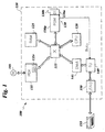
- a motor vehicle 100 has an engine 105; the operation of the engine 105 is managed by a control device 110 (which controls, for example, electronic injection, engine timing, and the like).
- the control device 110 is formed by various units which are connected selectively in pairs by means of an interconnection unit (cross-bar) 115.
- a central processing unit (CPU) 120 manages the operation of the control device 110
- a working memory (RAM) 125 is used directly by the CPU 120
- a non-volatile memory 130 contains programs and data for the operation of the CPU 120.
- the memory 130 which is produced in integrated form on a single chip of semiconductor material, is constituted by a flash E 2 PROM memory (erasable and reprogrammable in blocks); the flash memory 130 is a read-while-write memory so that it is possible to erase and reprogram one block whilst data is read from another block.
- a flash E 2 PROM memory erasable and reprogrammable in blocks
- the flash memory 130 is a read-while-write memory so that it is possible to erase and reprogram one block whilst data is read from another block.
- the flash memory 130 stores a control program for the CPU 120 and configuration parameters of the engine 105, typically organized in vectors and matrices of coherent data, that is, of data relating as a whole to the control of a particular function of the motor 105.
- the program (PGM) is stored in a dedicated portion 130p of the flash memory.
- the flash memory includes two further portions 130a and 130b; each portion 130a, 130b is used alternatively in an active state for storing a current version of the configuration parameters (read by the program executed by the CPU 120) or in an inactive state for the writing (as described in detail below) of a new version of the configuration parameters.
- a series of peripheral units 135 is also connected to the cross-bar 115; the peripheral units 135 consist, for example, of actuators for the regulation of the engine 105, or of sensors for measuring operating parameters thereof. Some of the peripheral units 135 (such as the actuators) have internal registers 135r which enable their operation to be regulated.
- the control device 100 also includes a calibration unit (TU) 140 with which a DMA (direct memory access) controller 145, directly connected to the cross-bar 115, is associated.
- a dedicated line is used to send, from the flash memory 130 to the calibration unit 140, a signal (busy) indicative of a writing operation in progress in the flash memory 130.
- the calibration unit 140 also communicates with an interface 150, for example, of the JTAG (Joint Test Access Group) type commonly used for testing the control device 110 and for periodic checking of its functionality.
- An external computer for example, a portable (laptop) computer 155, is connected to the control device 110 by means of a cable terminating in a PCMCIA connector inserted in a corresponding port associated with the JTAG interface 150.
- the JTAG interface 150 consists of a control logic unit which manages the serial transfer of data with one or more shift registers.
- the JTAG interface provides a line JTDI for receiving an input binary datum (bit), a line JTDO for sending an output bit, a line JTTMS for selecting a test mode, an initialization (reset) line JTRST, and a line JTCLK for sending a dedicated clock signal.
- the interface JTAG 150 is activated by the selection signal JTTMS, upon each leading edge of the clock signal JTCLK, the bit input on the line JTDI is recognized (strobed) and, upon each trailing edge of the clock signal JTCLK, a bit is output on the line JTDO.
- Both the CPU 120 and the DMA controller 145 operate in master mode for controlling access to the interconnection resources of the cross-bar 115 (within which there is an arbitrator which manages mutually exclusive access to the resources).
- These units have access to a memory space which is mapped in all of the resources of the control device 110 (the flash memory, the RAM memory, and the internal registers of the various units); in particular, the portion of the memory space which is dedicated to the current version of the configuration parameters (the current data space) is normally used by the CPU 120, whereas the portion of the memory space which is dedicated to the new version of the configuration parameters (data space being modified) is normally used by the DMA controller 145.
- the control program of the CPU 120 accesses the current version of the configuration parameters stored in one of the data portions 130a, 130b which is in the active state (for example, the data portion 130a).
- the CPU therefore controls the peripheral units 135 so as to send corresponding control signals to the engine 105.
- the CPU can interrogate (poll) the peripheral units 135 periodically, for example, every hour, to measure operating parameters of the engine 105.
- the operating parameters read are written in the other data portion of the flash memory which is in the inactive state (the portion 130b in the example in question).
- a corresponding interrupt signal for example, is sent to the CPU 120.
- the CPU consequently interrupts the storage of the operating parameters of the engine in the data portion 130b which is in the inactive state (whilst the reading of the configuration parameters from the portion 130a which is in the active state proceeds normally).
- the external computer 155 can thus load a command to read the operating parameters of the engine into the shift register of the JTAG interface 150.
- This read command is then supplied to the calibration unit 140 which manages the reading of the data portion 130b which is in the inactive state, directly by means of the DMA controller 145.
- the configuration parameters of the engine thus read are then supplied to the external computer 155 by the JTAG interface 150.
- the current version of the configuration parameter is downloaded to the external computer 155 in similar manner from the data portion 130a which is in the active state.
- the configuration parameters are modified in the external computer 155.
- the external computer 155 then loads a command to write a new configuration parameter in the shift register of the interface JTAG 150.
- the write command is then supplied to the calibration unit 140 which manages the writing of the data portion 130b which is in the inactive state, directly by means of the DMA controller 145.
- the flash memory 130 activates the busy signal; the calibration unit 140 does not therefore accept any subsequent command to write the flash memory until the writing operation in progress is completed (busy signal cancelled).
- the external computer 155 sends a corresponding writing-completed signal to the calibration unit 140 (by means of the JTAG interface 150).
- the states of the data portions 130a and 130b are consequently reversed; in the example in question, the data portion 130a switches to the inactive state and the data portion 130b switches to the active state.
- the management program of the CPU 120 thus automatically accesses the new version of the configuration parameters stored in the data portion 130b (whilst the other data portion 130a becomes available for further modification).
- the external computer 155 can also load a command to read the registers 135r into the shift register of the JTAG interface 150. This read command is then supplied to the calibration unit 140 which manages the reading of the registers 135b directly, by means of the DMA controller 145. The values thus read are then supplied to the external computer 155 by means of the JTAG interface 150.
- control device is used in a vehicle of a different type (for example, a motor cycle) or has a different structure (for example, with the various units connected in parallel to a bus), if the external computer is of a different type, for example, of the palmtop type, if it is connected to the control device by means of a connector of another type (for example, of the RJ45 type), or if the communication between the external computer and the control device uses a different protocol, and the like.
- the cross-bar 115 includes a multiplexer 205 having four inputs each of which is connected to one of the other connection ports of the cross-bar 115 (associated with the CPU, the RAM memory, the peripheral units and the DMA controller); the multiplexer 205 receives an address transmitted by the CPU or by the DMA controller to the respective connection port.
- the multiplexer 205 transmits this address (ADR) as an output in dependence on a selection signal (generated by the arbitrator of the cross-bar 115).
- a further multiplexer 210 has three inputs connected, respectively, to an output of the multiplexer 205, to an output of an adder 215a, and to an output of a subtractor 215b; the signal output by the multiplexer 210 is transferred to the port for connection to the flash memory.
- the adder 215a and the subtractor 215b receive, at respective inputs, the address ADR and an offset value OFS stored in a register 220; the offset OFS is equal to the difference between a first address of the data space being modified and a first address of the current data space.
- the address ADR is also supplied to a first input of a comparator 225a; a second input of the comparator 225a receives a signal (LMTa) stored in a register 230a.
- the address ADR is supplied to a first input of a further comparator 225b; a second input of the comparator 225b receives a signal (LMTb) stored in a further register 230b.
- the signal LMTa and the signal LMTb define the limits of the current data space and the limits of the data space being modified, respectively.
- the comparator 225a outputs a bit DTa indicative of the fact that the address ADR falls within the limits of the current data space; the comparator 225b outputs a bit DTb indicative of the fact that the address ADR falls within the limits of the data space being modified.
- the bit DTa and the bit DTb are supplied, respectively, to a first input of an AND logic gate 235a and to a first input of an AND logic gate 235b; the AND gates 235a and 235b receive, at respective second inputs, a flag SWP for inverting the memory mapping of the current data space and of the data space being modified.
- the AND gate 235a outputs a bit Sa and the AND gate outputs a bit Sb, and these are applied to respective selection inputs of the multiplexer 210.
- the corresponding bit Dta is set at logic level 1 (whilst the bit Dtb is cancelled).
- the bits Sa,Sb also adopt the value 00 in this case so that the address ADR is transferred as an output to the multiplexer 210 so as to access a corresponding location of a predetermined one of the data portions of the flash memory (for example, the first portion indicated 130a in Figure 1).
- the bit Sa adopts the value 1.
- the registers 220, 230a, 230b and 240 are set in response to an initialization (reset) command. Each time the calibration unit receives a writing-completed signal from the external computer, it sends an interrupt signal to the CPU 120. The CPU consequently performs a service routine which inverts the value of the flag SWP stored in the register 240 (so as to switch the states of the flash-memory data portions).
- the interrupt signal is preferably masked by the management program of the CPU during an operation to read a coherent data structure so as to be used only when all of the configuration parameters of the structure have been read.
- cross-bar has a different structure, if the functions described above are performed by other circuit components (possibly outside the cross-bar), and the like.
- the control device includes a first portion and a second portion of the memory unit each of which can be used alternatively in an active state for storing a current version of the configuration parameters or in an inactive state for the writing of a new version of the configuration parameters, the processing unit accessing the portion which is in the active state, for reading, and the input/output unit accessing the portion which is in the inactive state, for writing, and means for selectively switching one of the portions to the active state and the other of the portions to the inactive state.
- the management of the switching of the states of the portions of the flash memory by interruption is particularly quick and easy.
- the masking of the interrupt signal during the reading of a coherent data structure also ensures that the operating parameters used by the control device are modified only at safe moments, so as to ensure correct operation of the engine.
- the busy signal sent by the flash memory to the calibration unit enables the operation of the external computer (fast) to be synchronized with that of the flash memory (slow) without slowing down the operation of the control device in any way.
- the solution of the present invention may, however, also be implemented with two separate flash memories, with hardware switching of the states of the data portions (by means of two signals) without any control of the moment of switching, the external computer and the flash memory being synchronized by means of a flag (within the flash memory) which is indicative of the completion of the writing operation and is interrogated periodically by the calibration unit, and the like.
- the use of the JTAG interface enables functions already present in the control device to be utilized and does not require the addition of any new external connection terminals; moreover, this enables the external computer to be connected to the control device by standard connectors.
- the calibration unit with the respective DMA controller renders the writing of the new configuration parameters completely transparent to the external computer; this result is achieved independently of the CPU, with negligible slowing of the operation of the control device (due solely to any conflict with the CPU for access to the cross-bar).
- the calibration unit is not of the master type and the writing of the new configuration parameters in the flash memory is controlled directly by the CPU, the control device provides for a different input/output unit for connection to the external computer (with a dedicated interface and respective additional connection terminals), and the like.
Landscapes
- Engineering & Computer Science (AREA)
- Chemical & Material Sciences (AREA)
- Combustion & Propulsion (AREA)
- Mechanical Engineering (AREA)
- General Engineering & Computer Science (AREA)
- Computer Hardware Design (AREA)
- Microelectronics & Electronic Packaging (AREA)
- Physics & Mathematics (AREA)
- General Physics & Mathematics (AREA)
- Automation & Control Theory (AREA)
- Combined Controls Of Internal Combustion Engines (AREA)
- Control Of Electric Motors In General (AREA)
Priority Applications (2)
| Application Number | Priority Date | Filing Date | Title |
|---|---|---|---|
| BRPI0105641A BRPI0105641B1 (pt) | 2000-10-16 | 2001-10-15 | dispositivo de controle para um motor de veículo |
| US09/977,563 US6735514B2 (en) | 2000-10-16 | 2001-10-15 | Control device for a vehicle engine |
Applications Claiming Priority (2)
| Application Number | Priority Date | Filing Date | Title |
|---|---|---|---|
| WOPCT/IT00/00412 | 2000-10-16 | ||
| IT0000412 | 2000-10-16 |
Publications (3)
| Publication Number | Publication Date |
|---|---|
| EP1201899A2 true EP1201899A2 (de) | 2002-05-02 |
| EP1201899A3 EP1201899A3 (de) | 2003-11-26 |
| EP1201899B1 EP1201899B1 (de) | 2006-04-05 |
Family
ID=11133570
Family Applications (1)
| Application Number | Title | Priority Date | Filing Date |
|---|---|---|---|
| EP01101520A Expired - Lifetime EP1201899B1 (de) | 2000-10-16 | 2001-01-24 | Steuergerät für einen Kraftfahrzeugmotor |
Country Status (3)
| Country | Link |
|---|---|
| EP (1) | EP1201899B1 (de) |
| DE (1) | DE60118492T2 (de) |
| ES (1) | ES2260102T3 (de) |
Cited By (1)
| Publication number | Priority date | Publication date | Assignee | Title |
|---|---|---|---|---|
| WO2007015136A1 (en) * | 2005-08-01 | 2007-02-08 | Toyota Jidosha Kabusiki Kaisha | Robot control system and control method for robot |
Family Cites Families (4)
| Publication number | Priority date | Publication date | Assignee | Title |
|---|---|---|---|---|
| DE3018275A1 (de) * | 1980-05-13 | 1981-11-19 | Robert Bosch Gmbh, 7000 Stuttgart | Vorrichtung zur optimierung von daten und/oder programmen fuer programmierte steuergeraete |
| US5123397A (en) * | 1988-07-29 | 1992-06-23 | North American Philips Corporation | Vehicle management computer |
| WO1991007754A1 (en) * | 1989-11-13 | 1991-05-30 | Cray Research, Inc. | Read-while-write-memory |
| US6088264A (en) * | 1998-01-05 | 2000-07-11 | Intel Corporation | Flash memory partitioning for read-while-write operation |
-
2001
- 2001-01-24 EP EP01101520A patent/EP1201899B1/de not_active Expired - Lifetime
- 2001-01-24 DE DE60118492T patent/DE60118492T2/de not_active Expired - Lifetime
- 2001-01-24 ES ES01101520T patent/ES2260102T3/es not_active Expired - Lifetime
Cited By (1)
| Publication number | Priority date | Publication date | Assignee | Title |
|---|---|---|---|---|
| WO2007015136A1 (en) * | 2005-08-01 | 2007-02-08 | Toyota Jidosha Kabusiki Kaisha | Robot control system and control method for robot |
Also Published As
| Publication number | Publication date |
|---|---|
| EP1201899A3 (de) | 2003-11-26 |
| DE60118492T2 (de) | 2006-09-28 |
| DE60118492D1 (de) | 2006-05-18 |
| EP1201899B1 (de) | 2006-04-05 |
| ES2260102T3 (es) | 2006-11-01 |
Similar Documents
| Publication | Publication Date | Title |
|---|---|---|
| US4158227A (en) | Paged memory mapping with elimination of recurrent decoding | |
| EP0464433A2 (de) | Mikrocontroller mit fernprogrammierbarem EPROM und Programmierverfahren dafür | |
| KR100319733B1 (ko) | 불휘발성 반도체 메모리ic 및 그 번인 테스트 방법 | |
| US9092322B2 (en) | Processor system and control method thereof | |
| US5832251A (en) | Emulation device | |
| US5175831A (en) | System register initialization technique employing a non-volatile/read only memory | |
| US5903912A (en) | Microcontroller configured to convey data corresponding to internal memory accesses externally | |
| US6735514B2 (en) | Control device for a vehicle engine | |
| US20060178804A1 (en) | Control device for a motor vehicle and communication method therefor | |
| US5168559A (en) | Emulation system capable of complying with microcomputers having different on-chip memory capacities | |
| EP1480224A1 (de) | Ein Halbleiterspeicher mit serieller Multiprotokoll-Kommunikations-Schnittstelle | |
| US5860161A (en) | Microcontroller configured to indicate internal memory accesses externally | |
| EP1201899B1 (de) | Steuergerät für einen Kraftfahrzeugmotor | |
| EP2207100B1 (de) | System und Verfahren zur Datenwiederherstellung bei einer deaktivierten integrierten Schaltung | |
| US5644756A (en) | Integrated circuit data processor with selectable routing of data accesses | |
| US7028237B2 (en) | Internal bus testing device and method | |
| US6240377B1 (en) | Integrated circuit with embedded reprogrammable EEPROM and emulation method to facilitate debugging | |
| US5126972A (en) | Arrangement and method of ascertaining memory addresses which have been accessed during program execution | |
| KR20050110006A (ko) | 데이터 프로세싱 시스템의 메모리 관리 | |
| US5704048A (en) | Integrated microprocessor with internal bus and on-chip peripheral | |
| US5826059A (en) | Microcomputer for emulation | |
| US7743295B2 (en) | System and method for testing an integrated circuit | |
| KR0184154B1 (ko) | 원칩 마이크로 컴퓨터 | |
| JP2643803B2 (ja) | マイクロコンピュータ | |
| JP2000020340A (ja) | マイクロコンピュータ及びそのテスト方法 |
Legal Events
| Date | Code | Title | Description |
|---|---|---|---|
| PUAI | Public reference made under article 153(3) epc to a published international application that has entered the european phase |
Free format text: ORIGINAL CODE: 0009012 |
|
| AK | Designated contracting states |
Kind code of ref document: A2 Designated state(s): AT BE CH CY DE DK ES FI FR GB GR IE IT LI LU MC NL PT SE TR |
|
| AX | Request for extension of the european patent |
Free format text: AL;LT;LV;MK;RO;SI |
|
| PUAL | Search report despatched |
Free format text: ORIGINAL CODE: 0009013 |
|
| AK | Designated contracting states |
Kind code of ref document: A3 Designated state(s): AT BE CH CY DE DK ES FI FR GB GR IE IT LI LU MC NL PT SE TR |
|
| AX | Request for extension of the european patent |
Extension state: AL LT LV MK RO SI |
|
| 17P | Request for examination filed |
Effective date: 20040506 |
|
| 17Q | First examination report despatched |
Effective date: 20040701 |
|
| AKX | Designation fees paid |
Designated state(s): DE ES FR GB IT SE |
|
| GRAP | Despatch of communication of intention to grant a patent |
Free format text: ORIGINAL CODE: EPIDOSNIGR1 |
|
| GRAS | Grant fee paid |
Free format text: ORIGINAL CODE: EPIDOSNIGR3 |
|
| RIN1 | Information on inventor provided before grant (corrected) |
Inventor name: PEZZINI, SAVERIO Inventor name: PEPI, ALESSANDRO Inventor name: MARCECA, PAOLO Inventor name: FERRARI, ALBERTO |
|
| RAP1 | Party data changed (applicant data changed or rights of an application transferred) |
Owner name: MAGNETI MARELLI POWERTRAIN S.P.A. Owner name: STMICROELECTRONICS S.R.L. |
|
| GRAA | (expected) grant |
Free format text: ORIGINAL CODE: 0009210 |
|
| AK | Designated contracting states |
Kind code of ref document: B1 Designated state(s): DE ES FR GB IT SE |
|
| PG25 | Lapsed in a contracting state [announced via postgrant information from national office to epo] |
Ref country code: IT Free format text: LAPSE BECAUSE OF FAILURE TO SUBMIT A TRANSLATION OF THE DESCRIPTION OR TO PAY THE FEE WITHIN THE PRESCRIBED TIME-LIMIT;WARNING: LAPSES OF ITALIAN PATENTS WITH EFFECTIVE DATE BEFORE 2007 MAY HAVE OCCURRED AT ANY TIME BEFORE 2007. THE CORRECT EFFECTIVE DATE MAY BE DIFFERENT FROM THE ONE RECORDED. Effective date: 20060405 |
|
| REG | Reference to a national code |
Ref country code: GB Ref legal event code: FG4D |
|
| REF | Corresponds to: |
Ref document number: 60118492 Country of ref document: DE Date of ref document: 20060518 Kind code of ref document: P |
|
| REG | Reference to a national code |
Ref country code: SE Ref legal event code: TRGR |
|
| ET | Fr: translation filed | ||
| REG | Reference to a national code |
Ref country code: ES Ref legal event code: FG2A Ref document number: 2260102 Country of ref document: ES Kind code of ref document: T3 |
|
| PLBE | No opposition filed within time limit |
Free format text: ORIGINAL CODE: 0009261 |
|
| STAA | Information on the status of an ep patent application or granted ep patent |
Free format text: STATUS: NO OPPOSITION FILED WITHIN TIME LIMIT |
|
| 26N | No opposition filed |
Effective date: 20070108 |
|
| REG | Reference to a national code |
Ref country code: FR Ref legal event code: PLFP Year of fee payment: 16 |
|
| REG | Reference to a national code |
Ref country code: FR Ref legal event code: PLFP Year of fee payment: 17 |
|
| REG | Reference to a national code |
Ref country code: FR Ref legal event code: PLFP Year of fee payment: 18 |
|
| PGFP | Annual fee paid to national office [announced via postgrant information from national office to epo] |
Ref country code: SE Payment date: 20191227 Year of fee payment: 20 |
|
| PGFP | Annual fee paid to national office [announced via postgrant information from national office to epo] |
Ref country code: FR Payment date: 20191219 Year of fee payment: 20 |
|
| PGFP | Annual fee paid to national office [announced via postgrant information from national office to epo] |
Ref country code: IT Payment date: 20200102 Year of fee payment: 20 Ref country code: DE Payment date: 20191218 Year of fee payment: 20 Ref country code: ES Payment date: 20200203 Year of fee payment: 20 Ref country code: GB Payment date: 20191223 Year of fee payment: 20 |
|
| REG | Reference to a national code |
Ref country code: DE Ref legal event code: R071 Ref document number: 60118492 Country of ref document: DE |
|
| REG | Reference to a national code |
Ref country code: GB Ref legal event code: PE20 Expiry date: 20210123 |
|
| REG | Reference to a national code |
Ref country code: SE Ref legal event code: EUG |
|
| PG25 | Lapsed in a contracting state [announced via postgrant information from national office to epo] |
Ref country code: GB Free format text: LAPSE BECAUSE OF EXPIRATION OF PROTECTION Effective date: 20210123 |
|
| REG | Reference to a national code |
Ref country code: ES Ref legal event code: FD2A Effective date: 20220128 |
|
| PG25 | Lapsed in a contracting state [announced via postgrant information from national office to epo] |
Ref country code: ES Free format text: LAPSE BECAUSE OF EXPIRATION OF PROTECTION Effective date: 20210125 |