EP1201108B1 - A circuit singulation system and method - Google Patents
A circuit singulation system and method Download PDFInfo
- Publication number
- EP1201108B1 EP1201108B1 EP00948225A EP00948225A EP1201108B1 EP 1201108 B1 EP1201108 B1 EP 1201108B1 EP 00948225 A EP00948225 A EP 00948225A EP 00948225 A EP00948225 A EP 00948225A EP 1201108 B1 EP1201108 B1 EP 1201108B1
- Authority
- EP
- European Patent Office
- Prior art keywords
- cut
- laser
- laser beam
- cutting
- wavelength
- Prior art date
- Legal status (The legal status is an assumption and is not a legal conclusion. Google has not performed a legal analysis and makes no representation as to the accuracy of the status listed.)
- Expired - Lifetime
Links
Images



Classifications
-
- H—ELECTRICITY
- H05—ELECTRIC TECHNIQUES NOT OTHERWISE PROVIDED FOR
- H05K—PRINTED CIRCUITS; CASINGS OR CONSTRUCTIONAL DETAILS OF ELECTRIC APPARATUS; MANUFACTURE OF ASSEMBLAGES OF ELECTRICAL COMPONENTS
- H05K3/00—Apparatus or processes for manufacturing printed circuits
- H05K3/0011—Working of insulating substrates or insulating layers
- H05K3/0017—Etching of the substrate by chemical or physical means
- H05K3/0026—Etching of the substrate by chemical or physical means by laser ablation
- H05K3/0032—Etching of the substrate by chemical or physical means by laser ablation of organic insulating material
-
- B—PERFORMING OPERATIONS; TRANSPORTING
- B23—MACHINE TOOLS; METAL-WORKING NOT OTHERWISE PROVIDED FOR
- B23K—SOLDERING OR UNSOLDERING; WELDING; CLADDING OR PLATING BY SOLDERING OR WELDING; CUTTING BY APPLYING HEAT LOCALLY, e.g. FLAME CUTTING; WORKING BY LASER BEAM
- B23K26/00—Working by laser beam, e.g. welding, cutting or boring
- B23K26/36—Removing material
- B23K26/40—Removing material taking account of the properties of the material involved
-
- H—ELECTRICITY
- H10—SEMICONDUCTOR DEVICES; ELECTRIC SOLID-STATE DEVICES NOT OTHERWISE PROVIDED FOR
- H10P—GENERIC PROCESSES OR APPARATUS FOR THE MANUFACTURE OR TREATMENT OF DEVICES COVERED BY CLASS H10
- H10P72/00—Handling or holding of wafers, substrates or devices during manufacture or treatment thereof
- H10P72/04—Apparatus for manufacture or treatment
- H10P72/0428—Apparatus for mechanical treatment or grinding or cutting
-
- H—ELECTRICITY
- H10—SEMICONDUCTOR DEVICES; ELECTRIC SOLID-STATE DEVICES NOT OTHERWISE PROVIDED FOR
- H10W—GENERIC PACKAGES, INTERCONNECTIONS, CONNECTORS OR OTHER CONSTRUCTIONAL DETAILS OF DEVICES COVERED BY CLASS H10
- H10W99/00—Subject matter not provided for in other groups of this subclass
-
- B—PERFORMING OPERATIONS; TRANSPORTING
- B23—MACHINE TOOLS; METAL-WORKING NOT OTHERWISE PROVIDED FOR
- B23K—SOLDERING OR UNSOLDERING; WELDING; CLADDING OR PLATING BY SOLDERING OR WELDING; CUTTING BY APPLYING HEAT LOCALLY, e.g. FLAME CUTTING; WORKING BY LASER BEAM
- B23K2101/00—Articles made by soldering, welding or cutting
- B23K2101/36—Electric or electronic devices
- B23K2101/40—Semiconductor devices
-
- B—PERFORMING OPERATIONS; TRANSPORTING
- B23—MACHINE TOOLS; METAL-WORKING NOT OTHERWISE PROVIDED FOR
- B23K—SOLDERING OR UNSOLDERING; WELDING; CLADDING OR PLATING BY SOLDERING OR WELDING; CUTTING BY APPLYING HEAT LOCALLY, e.g. FLAME CUTTING; WORKING BY LASER BEAM
- B23K2103/00—Materials to be soldered, welded or cut
- B23K2103/50—Inorganic materials other than metals or composite materials
-
- H—ELECTRICITY
- H05—ELECTRIC TECHNIQUES NOT OTHERWISE PROVIDED FOR
- H05K—PRINTED CIRCUITS; CASINGS OR CONSTRUCTIONAL DETAILS OF ELECTRIC APPARATUS; MANUFACTURE OF ASSEMBLAGES OF ELECTRICAL COMPONENTS
- H05K1/00—Printed circuits
- H05K1/02—Details
- H05K1/0266—Marks, test patterns or identification means
- H05K1/0269—Marks, test patterns or identification means for visual or optical inspection
-
- H—ELECTRICITY
- H05—ELECTRIC TECHNIQUES NOT OTHERWISE PROVIDED FOR
- H05K—PRINTED CIRCUITS; CASINGS OR CONSTRUCTIONAL DETAILS OF ELECTRIC APPARATUS; MANUFACTURE OF ASSEMBLAGES OF ELECTRICAL COMPONENTS
- H05K2201/00—Indexing scheme relating to printed circuits covered by H05K1/00
- H05K2201/09—Shape and layout
- H05K2201/09818—Shape or layout details not covered by a single group of H05K2201/09009 - H05K2201/09809
- H05K2201/09918—Optically detected marks used for aligning tool relative to the PCB, e.g. for mounting of components
-
- H—ELECTRICITY
- H05—ELECTRIC TECHNIQUES NOT OTHERWISE PROVIDED FOR
- H05K—PRINTED CIRCUITS; CASINGS OR CONSTRUCTIONAL DETAILS OF ELECTRIC APPARATUS; MANUFACTURE OF ASSEMBLAGES OF ELECTRICAL COMPONENTS
- H05K3/00—Apparatus or processes for manufacturing printed circuits
- H05K3/0008—Apparatus or processes for manufacturing printed circuits for aligning or positioning of tools relative to the circuit board
-
- H—ELECTRICITY
- H05—ELECTRIC TECHNIQUES NOT OTHERWISE PROVIDED FOR
- H05K—PRINTED CIRCUITS; CASINGS OR CONSTRUCTIONAL DETAILS OF ELECTRIC APPARATUS; MANUFACTURE OF ASSEMBLAGES OF ELECTRICAL COMPONENTS
- H05K3/00—Apparatus or processes for manufacturing printed circuits
- H05K3/0011—Working of insulating substrates or insulating layers
- H05K3/0017—Etching of the substrate by chemical or physical means
- H05K3/0026—Etching of the substrate by chemical or physical means by laser ablation
- H05K3/0032—Etching of the substrate by chemical or physical means by laser ablation of organic insulating material
- H05K3/0038—Etching of the substrate by chemical or physical means by laser ablation of organic insulating material combined with laser drilling through a metal layer
-
- H—ELECTRICITY
- H05—ELECTRIC TECHNIQUES NOT OTHERWISE PROVIDED FOR
- H05K—PRINTED CIRCUITS; CASINGS OR CONSTRUCTIONAL DETAILS OF ELECTRIC APPARATUS; MANUFACTURE OF ASSEMBLAGES OF ELECTRICAL COMPONENTS
- H05K3/00—Apparatus or processes for manufacturing printed circuits
- H05K3/0011—Working of insulating substrates or insulating layers
- H05K3/0044—Mechanical working of the substrate, e.g. drilling or punching
- H05K3/0052—Depaneling, i.e. dividing a panel into circuit boards; Working of the edges of circuit boards
-
- H—ELECTRICITY
- H10—SEMICONDUCTOR DEVICES; ELECTRIC SOLID-STATE DEVICES NOT OTHERWISE PROVIDED FOR
- H10P—GENERIC PROCESSES OR APPARATUS FOR THE MANUFACTURE OR TREATMENT OF DEVICES COVERED BY CLASS H10
- H10P72/00—Handling or holding of wafers, substrates or devices during manufacture or treatment thereof
- H10P72/70—Handling or holding of wafers, substrates or devices during manufacture or treatment thereof for supporting or gripping
- H10P72/74—Handling or holding of wafers, substrates or devices during manufacture or treatment thereof for supporting or gripping using temporarily an auxiliary support
- H10P72/741—Handling or holding of wafers, substrates or devices during manufacture or treatment thereof for supporting or gripping using temporarily an auxiliary support the auxiliary support including a cavity for storing a finished or partly finished device during manufacturing or mounting, e.g. for an IC package or for a chip
-
- H—ELECTRICITY
- H10—SEMICONDUCTOR DEVICES; ELECTRIC SOLID-STATE DEVICES NOT OTHERWISE PROVIDED FOR
- H10W—GENERIC PACKAGES, INTERCONNECTIONS, CONNECTORS OR OTHER CONSTRUCTIONAL DETAILS OF DEVICES COVERED BY CLASS H10
- H10W46/00—Marks applied to devices, e.g. for alignment or identification
- H10W46/601—Marks applied to devices, e.g. for alignment or identification for use after dicing
- H10W46/607—Located on parts of packages, e.g. on encapsulations or on package substrates
-
- H—ELECTRICITY
- H10—SEMICONDUCTOR DEVICES; ELECTRIC SOLID-STATE DEVICES NOT OTHERWISE PROVIDED FOR
- H10W—GENERIC PACKAGES, INTERCONNECTIONS, CONNECTORS OR OTHER CONSTRUCTIONAL DETAILS OF DEVICES COVERED BY CLASS H10
- H10W72/00—Interconnections or connectors in packages
- H10W72/01—Manufacture or treatment
- H10W72/0198—Manufacture or treatment batch processes
-
- H—ELECTRICITY
- H10—SEMICONDUCTOR DEVICES; ELECTRIC SOLID-STATE DEVICES NOT OTHERWISE PROVIDED FOR
- H10W—GENERIC PACKAGES, INTERCONNECTIONS, CONNECTORS OR OTHER CONSTRUCTIONAL DETAILS OF DEVICES COVERED BY CLASS H10
- H10W72/00—Interconnections or connectors in packages
- H10W72/071—Connecting or disconnecting
- H10W72/072—Connecting or disconnecting of bump connectors
- H10W72/07251—Connecting or disconnecting of bump connectors characterised by changes in properties of the bump connectors during connecting
-
- H—ELECTRICITY
- H10—SEMICONDUCTOR DEVICES; ELECTRIC SOLID-STATE DEVICES NOT OTHERWISE PROVIDED FOR
- H10W—GENERIC PACKAGES, INTERCONNECTIONS, CONNECTORS OR OTHER CONSTRUCTIONAL DETAILS OF DEVICES COVERED BY CLASS H10
- H10W72/00—Interconnections or connectors in packages
- H10W72/20—Bump connectors, e.g. solder bumps or copper pillars; Dummy bumps; Thermal bumps
-
- H—ELECTRICITY
- H10—SEMICONDUCTOR DEVICES; ELECTRIC SOLID-STATE DEVICES NOT OTHERWISE PROVIDED FOR
- H10W—GENERIC PACKAGES, INTERCONNECTIONS, CONNECTORS OR OTHER CONSTRUCTIONAL DETAILS OF DEVICES COVERED BY CLASS H10
- H10W74/00—Encapsulations, e.g. protective coatings
- H10W74/10—Encapsulations, e.g. protective coatings characterised by their shape or disposition
- H10W74/131—Encapsulations, e.g. protective coatings characterised by their shape or disposition the semiconductor body being only partially enclosed
- H10W74/142—Encapsulations, e.g. protective coatings characterised by their shape or disposition the semiconductor body being only partially enclosed the encapsulations exposing the passive side of the semiconductor body
Definitions
- the invention relates to a method and machine to cut circuit boards or integrated circuit packages.
- circuit boards are becoming lighter and smaller.
- the materials from which integrated circuit packages or circuit boards are fabricated may include, for example, copper layers, glass fiber layers or weave, FR4, BT glass/epoxy, adhesives, encapsulants, solder masks or semiconductor.
- Another type of circuit board is a polymer-based flexible (flex) circuit.
- the invention may be applied to cut thin layers such as liquid crystal sheets or electrochromic dielectric thin films as used in displays.
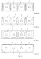
- Figs. 1A(a) to 1A(d) show examples of strips on which several BGA devices are mounted.
- encapsulant material 1 protects the die 2 and the electrical connections between the die and the substrate 3.
- the assembly process may require the presence of tooling holes and cut out sections 4 for ease of punching.
- the strip of Fig. 1A(c) is similar to that of Fig.1A(a) except that cut out strips are missing, and in the strip of Fig. 1A(c) there are no tooling holes.
- the encapsulant covers multiple dies. In this situation, BGA singulation requires that the encapsulant be cut also.
- the dashed lines 5 in the drawings indicate the cutting lines to singulate individual packages.
- FIG. 1B A further example of a multiple unit, chip-scale package assembly is shown in Fig. 1B.
- dies are mounted on a substrate in two dimensions to form an N x N assembly of BGA packages 6.
- Fig. 1B shows the underside of the assembly.
- Solder balls 7 are positioned at the correct position on the circuit board and are then reflowed. The reflowed solder balls then form the electrical contact between the circuit board and the package.
- the electrical connection to the die is through the package substrate.
- the substrate layers may be copper layers, glass fiber layers or weave, FR4, BT glass/epoxy, adhesives, encapsulants, solder masks or semiconductor. Referring to the end view in Fig. 1B the substrate often comprises multiple layers which may include solder mask 8, copper 9, dielectric 10, glass 11, and epoxy 12. Gold or another conductor may be used in the layer 9 instead of copper.
- Fig. 1C shows an example of a circuit board panel containing multiple circuit boards 21. Such panels may be those used for "smart cards" or mobile telephone circuits.
- the circuit board material may be rigid or flexible material made from laminated layers of copper layers, glass fiber layers or weave, FR4, BT glass/epoxy, adhesives, encapsulants, solder masks, or other materials used in circuit board manufacture.
- the circuit board may be of a flexible material.
- This type of circuit generally is made from layers of copper, adhesive and polymer such as Kapton polyimide or another polymer with the required mechanical properties.
- liquid crystal electro- chromic or more generally, thin film sheeting in liquid crystal displays or in mass-produced display assemblies.
- Fig. 1D shows the final steps involved in the present method of manufacturing of BGA/CSP devices. Due to the nature of the devices and systems involved, several handling and cleaning steps must be added in order to support the singulation process with wafer saws. The steps include:
- US-A-5 928 526 and US-A-5 500 505 show methods for singulating a circuit by cutting with a laser.
- An object of the invention is to provide a system and a method to cut through the above materials at a rate sufficient to meet the singulation rate requirements for a production line.
- Another object is that the method and apparatus provide a higher yield by reducing the extent of deposited debris and by reducing handling requirements.
- beam is moved to have a spatial overlap of consecutive pulses, the overlap being in the range of 5% to 95%.
- the overlap is in the range of 30% to 50%.
- the beam is moved in a plurality of passes.
- the beam is moved in greater than five passes.
- the beam is generated with a pulse repetition rate of greater than 1kHz.
- the thickness of the laminated structures may be up to the thickness defined by the depth of focus of the laser beam.
- the laminate material contains two or more layers selected from BT epoxy, glass fibers, copper, gold, poly-imide, adhesive, overmold materials, underfills, conductors, dielectrics, stiffeners, stabilisers, protectors or other materials as used in electronic packaging.
- the individual layers of the laminate material have different ablation and ionization thresholds, different abalation and ionization rates, and different non-linear absorption and non-ionization coefficients.
- the beam is generated from a solid state laser with a characteristic average power peak at a specific repetition frequency.
- the beam is controlled so that the average power drops as the repetition frequency is increased or decreased, and although individual pulse energy may be increased at a repetition frequency other than the repetition frequency for maximum average power the maximum cut rate is achieved at a repetition frequency other than either of these frequencies due to the contribution of other laser cutting parameters.
- the average power of said laser beam is greater than 3W, with a pulse width less than 100 nanoseconds, a consecutive pulse spatial overlap of 10-70%, and a beam diameter less than 70 microns at the 1/e 2 point of a spatial intensity profile.
- the laser beam is generated by a diode laser pumped gain medium device with a fundamental emission in the 900 to 1600nm wavelength range and with second, third, fourth or fifth harmonic generation of 1 ⁇ 2, 1/3, 1 ⁇ 4, 1/5 th of this wavelength which is obtained by placing appropriate crystals in the laser cavity or outside the laser cavity.
- said laser device may be of the Nd: YAG, ND: YLF, Nd:YVO4 or the other combinations of Impurity:Host gain media lasing in the required range and with harmonic generation to an operating wavelength of less than 400nm.
- the beam is delivered to the work surface using one or more mirrors mounted on one or more scanning galvanometers, and in which the required spot size is achieved by use of an on-axis lens position adjustment at a stage before the galvanometer mirror, and at a stage after the galvanometer mirror by a lens of a flat field lens, or by the use of a combination of these lenses.
- the laser beam is delivered using one or more minors mounted on one or more translational stages, and focusing is achieved by the use of a telescope or an on-axis lens before the moving mirrors or lens mounted before the sample surface and moving with the beam delivery mirror such that the focussed beam is delivered to the sample surface.
- the beam is telescoped and focussed to achieve the required spot size at the cutting plane with the telescope or scan lens chosen such that the beam waist remains within a specified percentage of the optimum spot size throughout the range over which the beam is delivered, and wherein the range is greater than the thickness of the part.
- an assist gas is used to assist the cutting process to prevent debris from being deposited on the material surface, and wherein the assist gas removes material generated during the cut process so that it does not create absorption or scattering of consecutive laser light pulses.
- the assist gas is used to provide an inert atmosphere to prevent unwanted specific photochemical or photo-physical reactions form occurring during cutting.
- a vacuum suction process is used to extract fumes and solid debris generated at the cut surface.
- alignment of the laser beam to a feature on the material surface is achieved by use of a sensor and means for image processing to provide the coordinates along which cutting occurs, and wherein a beam positioning mechanism is controlled to ensure that the laser beam follows the required cutting path.
- the invention provides a circuit singulation system comprising:
- the beam positioning system comprises a series of mirrors, at least some of which are movable for directing the laser beam, and a focusing lens.
- the mirrors are linearly movable.
- the mirrors are rotatable.
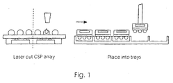
- the invention is based upon use of a laser beam for singulation, as shown in Fig. 1.
- the process uses an ultraviolet laser to "saw” the package.
- the laser creates excellent quality cuts which generate only vapor debris, use no consumables, and do not cause any chips or micro-cracks in the cut edges.
- the apparatus of the invention uses an ultra-violet solid state laser to cut materials that form chip scale packages such as ball grid arrays, circuit board materials and other "thin film” type materials that may form the lamellae of such laminated packages.
- Solid state YAG/YLF and NVO4 lasers and other lasers operating with fundamental laser emission in the visible or infra red may be converted to ultraviolet lasers through second and third harmonic generation, sum and difference frequency mixing in second order nonlinear crystals.
- the apparatus consists of an ultraviolet laser system as described above, and a beam positioning mechanism.
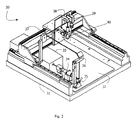
- the beam positioning mechanism may be a multiple axis stage as illustrated in Fig. 2 or a scanning galvanometer as illustrated in Fig. 3.
- a frame 31 supports a target 32 to be singulated.
- the optical path is:-
- the cut process may be monitored in real time by observing the light energy reflected from the surface of the material being cut back-reflected along the path of the incident beam and on to a photo-electric detector. In the event that the material has been completely cut, there will be no reflective surface and the signal at the detector will drop to a background level, ideally zero.
- the reflected light may be U.V. laser light, in which case a beam splitter for the laser wavelength is used.
- a mirror transparent to Ultraviolet e.g. 355nm
- the second harmonic wavelength e.g. 532nm
- the feedback mechanism is the visible to infrared emission of the plume generated during the cutting process. In the absence of this plume, no cutting occurs and the sample has been cut through. The presence of the plume may be taken as evidence that cutting is occurring. Furthermore, the spectral content of the plume provides information on the material that is being cut.
- Real time control of cutting multi-layer materials is possible by monitoring the spectral output at each position of the pulse on the cut scan. From the control point, once the signal can be delivered and processed before the next measurement occurs it is possible to control the laser output parameters on a pulse to pulse basis. This is beneficial in the case where composite materials such as laminated packages may have variations in material distribution across the cut surface. In addition, once a layer has been completely cut through the laser parameters can be varied on the fly such that the cut process is optimised for the next layer.
- a second option for beam delivery and position control is to use a scanning galvanometer.
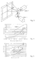
- Fig. 3 shows the essential geometry. Two mirrors are mounted on current driven galvanometer coils that rotate the axes on which the mirror is mounted. Scanning from position A to position D can be achieved by scanning galvanometer Galv.1 through an angle G1 with galvanometer Galv.2 oriented so that its mirror reflects along this line. Scanning from position A to position B may be achieved by rotating galvanometer Galv.2 through an angle G2 with galvanometer Galv.1 fixed for position A on the AD line. Accordingly, any position in two dimensions may be marked out by a combination of moves of the two mirrors.
- the galvanometer approach allows high acceleration and deceleration times, resulting in minimal time between moves and minimal effect on processing time.
- a combination of a galvanometer and XY stage or gantry approach can provide this.
- a specimen may be mounted on an XY stage below a galvanometer arrangement.
- High speed and acceleration is possible over a small area with a high degree of accuracy through the galvo action and slower moves with high accuracy are possible with the XY stage. Where the number of slower moves is low, the overall effect on processing time will be negligible.
- This galvo/XY stage combination allows accuracy and speed to be exploited.
- the type of laser, the laser output specifications, the beam delivery method and the material that is to be cut all affect the rate at which the material is cut and the quality of the resulting cut.
- the optical configuration described above delivers a laser beam to the surface to be cut.
- the beam is focussed to a small diameter, high-intensity spot.
- the laser fires pulses in sequence at rates greater than 1 kHz.
- Cutting is achieved by scanning the beam over the sample (or scanning the sample through the beam) at a speed such that there is sufficient overlap between the pulses to allow cutting.
- Pulse energy is the energy within a single pulse of the pulse train, and the energy density is the value per cm 2 .
- Repetition frequency defines the number of pulses per second.
- Scan speed The scan speed of the laser relative to the sample is defined by the required spatial overlap for a given spot size at a fixed repetition rate.
- Overlap The overlap is defined as the percentage of the beam diameter that overlaps spatially with the other pulses in sequence.
- the spot size or beam diameter determines the peak power density(W/cm2) and fluence (J/cm2) at the cutting surface. Also, the spot size determines at which velocity the laser should be scanned relative to the sample to achieve the required overlap.
- Peak power density is the peak power delivered per unit area (cm 2 ).
- the linear absorption coefficient, ⁇ determines the penetration depth of the pulse.
- Nonlinear absorption processes include absorption saturation, inverse saturable absorption, and photo-ionisation.
- an assist gas it is possible to ensure that debris is not redepositied on the sample surface. Also, some gases may enhance photo- removal of material and others may suppress unwanted non-clean chemical processes.
- the cut rate increases linearly or "super" linearly as pulse energy is increased.
- a further parameter that affects the beam energy/power density at the sample is the beam diameter. Focussing to a smaller beam waist at the sample results in an increase in the peak power density, average power density and energy density at the sample. All of these result in an increase in material removal. Eventually, however, the "kerf" or width of the cutting region physically occludes material removal and it is necessary to ensure a sufficient kerf width to maintain the material removal rate. A second factor which must be taken into account is the depth of field. Focussing too tightly will reduce the depth of field. Finally, reproducibility of the positioning system will become critical at smaller beam sizes. With these factors in mind, the optimum beam diameter lies in the range from 8 to 70 microns.
- the parameter space is then defined by (in no particular order):
- Example 1 Flex circuit packages and liquid crystal sheet
- the laser was a frequency tripled Q-switched Nd: Yag laser.
- the laser stability was better than 7% about the mean and the mode operation was in the fundamental TEM 00.
- the operating specification is shown in Table 2.
- Laser parameters for Example 1 Parameter Value Wavelength 355nm Average power 4W Pulse-width 95 ns Rep Rate 5.5kHz Pulse energy 0.727mJ Fluence 148 J/cm2 Peak Power 7.7KW Peak Power density 1.56 GW/cm 2
- the cutting parameters for five representative flex circuit materials were used.
- the samples consist of solder mask, poly-imide and adhesive in various laminations.
- Sample #1 Contains 5 layers of material. 2-poly-imide, 2-adhesive, 1- solder mask. Sample #1A: Sample is identical to sample # 1 except for the continuation of the solder mask over the heat bond area on one side.
- Sample #2 Sample contains 3 layers of material. 1-poly-imide, 2-solder mask.
- Sample #3 Sample contains 5 layers in the non-copper loaded areas. 3-poly-imide, 2-adhesive
- Sample #4 Sample contains 3 layers of material(1-liquid crystal polymer, 2-solder mask
- the optimum rep rate was established by varying the rep rate and scan speed, ensuring similar overlap and counting the number of passes required to machine through. Although the rep rate could be tuned up to 15kHz the optimum machining performance is obtained when the average power is near the peak. At this point the individual pulse energy may not be at a maximum but the total delivered energy is such that that cutting occurs in the fastest possible time.
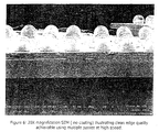
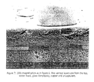
- the cut rate for a 1mm thick overmolded BGA package was measured as 4.2mm /sec at 3W average power. This was accomplished by using 24 passes at a speed of 100mm/s ( approx. 50% overlap at the FWHM intensity point). 20X and 100X SEM images of the edges obtained are shown in Figs. 6 and 7 respectively.
- the sample consists of solder mask, glass fiber matrix, epoxy and adhesive, copper and encapsulant regions. It is clear that the edge quality is defect free. The open space that appears is likely due to the free volume of the encapsulant material.
- the laser cutting process does not incur costs associated with wafer saw, for UV tape deionised water, drying, and for saw consumables.
- Laser excising consumes less space in class 1000 clean room area. Laser excising and inspection require only approximately 2 square metre, as opposed to approximately 5 square metres for prior art sawing, handling, and inspection equipment.
- the excising method of the invention results in much smaller "kerf". Typically in the prior art methods saws are given 250 ⁇ m waste area and use 175um cuts. In the invention, the waste area is 25 ⁇ m or less. Thus, the invention achieves greater "real estate" for components, particularly small components. Also, the invention achieves edges with less stress and no micro-cracking.
Landscapes
- Engineering & Computer Science (AREA)
- Physics & Mathematics (AREA)
- Optics & Photonics (AREA)
- Manufacturing & Machinery (AREA)
- Microelectronics & Electronic Packaging (AREA)
- Plasma & Fusion (AREA)
- Mechanical Engineering (AREA)
- Laser Beam Processing (AREA)
- Dicing (AREA)
- Electrotherapy Devices (AREA)
- Mobile Radio Communication Systems (AREA)
Abstract
Description
- The invention relates to a method and machine to cut circuit boards or integrated circuit packages.
- In recent years, in the microelectronics industry there has been a drive for lightweight, low profile consumer electronics products such as laptop computers and mobile telephones. These consumer electronics products require high-throughput assembly of low-cost, low-profile and lightweight integrated circuit packages. Integrated circuits are packaged in multiple units to achieve the required throughput and to reduce handling requirements. At the end of this process it is then necessary to singulate the packaged devices.
- By reducing the area of the integrated circuit package it is also possible to reduce the area of the circuit boards on which these devices will perform their function. To this end, circuit boards are becoming lighter and smaller.
- The materials from which integrated circuit packages or circuit boards are fabricated may include, for example, copper layers, glass fiber layers or weave, FR4, BT glass/epoxy, adhesives, encapsulants, solder masks or semiconductor. Another type of circuit board, is a polymer-based flexible (flex) circuit. Also, the invention may be applied to cut thin layers such as liquid crystal sheets or electrochromic dielectric thin films as used in displays.
- Figs. 1A(a) to 1A(d) show examples of strips on which several BGA devices are mounted. In Fig.1A(a) encapsulant material 1 protects the die 2 and the electrical connections between the die and the substrate 3. The assembly process may require the presence of tooling holes and cut out sections 4 for ease of punching. The strip of Fig. 1A(c) is similar to that of Fig.1A(a) except that cut out strips are missing, and in the strip of Fig. 1A(c) there are no tooling holes. In the strip of Fig 1A(d) the encapsulant covers multiple dies. In this situation, BGA singulation requires that the encapsulant be cut also. The dashed lines 5 in the drawings indicate the cutting lines to singulate individual packages.
- A further example of a multiple unit, chip-scale package assembly is shown in Fig. 1B. In this example dies are mounted on a substrate in two dimensions to form an N x N assembly of BGA packages 6. Fig. 1B shows the underside of the assembly. Solder balls 7 are positioned at the correct position on the circuit board and are then reflowed. The reflowed solder balls then form the electrical contact between the circuit board and the package. The electrical connection to the die is through the package substrate. The substrate layers may be copper layers, glass fiber layers or weave, FR4, BT glass/epoxy, adhesives, encapsulants, solder masks or semiconductor. Referring to the end view in Fig. 1B the substrate often comprises multiple layers which may include solder mask 8, copper 9, dielectric 10, glass 11, and epoxy 12. Gold or another conductor may be used in the layer 9 instead of copper.
- Fig. 1C shows an example of a circuit board panel containing multiple circuit boards 21. Such panels may be those used for "smart cards" or mobile telephone circuits. The circuit board material may be rigid or flexible material made from laminated layers of copper layers, glass fiber layers or weave, FR4, BT glass/epoxy, adhesives, encapsulants, solder masks, or other materials used in circuit board manufacture.
- The circuit board may be of a flexible material. This type of circuit generally is made from layers of copper, adhesive and polymer such as Kapton polyimide or another polymer with the required mechanical properties.
- The electronics industry also uses liquid crystal, electro- chromic or more generally, thin film sheeting in liquid crystal displays or in mass-produced display assemblies.
- Regarding the present methods of singulation, Fig. 1D shows the final steps involved in the present method of manufacturing of BGA/CSP devices. Due to the nature of the devices and systems involved, several handling and cleaning steps must be added in order to support the singulation process with wafer saws. The steps include:
- electrical test and laser mark in boats, panels or trays,
- removal from boat or tray and mounting on tacky UV tape ,
- cutting with saw and cleaning,
- UV cure,
- placing on trays,
- marking and inspection.
-
- Sawing and punching of chip scale packages is described in WO9903128: (Singulation system for chip scale packages) and in WO98/52212: (Pick and place cutting head that separates chip scale packages from a Multi layered film strip). Several consumables, such as UV tape, wafer rings, saw blades, and cleaning solutions must be used.
- US-A-5 928 526 and US-A-5 500 505 show methods for singulating a circuit by cutting with a laser.
- An object of the invention is to provide a system and a method to cut through the above materials at a rate sufficient to meet the singulation rate requirements for a production line.
- Another object is that the method and apparatus provide a higher yield by reducing the extent of deposited debris and by reducing handling requirements.
- According to the invention, there is provided a method for singulating an electronic circuit by cutting laminated material joining the circuits, the method comprising the steps of:-
- generating a laser beam having the following properties:
- a wavelength of less than 400nm, and
- a minimum energy density of 100 J/cm2 or a minimum peak power
- density of 1GW/cm2;
- aligning the beam relative to a feature or fiducial of the material; and
- training the beam along the material until a cut has been made.
-
- In one embodiment, beam is moved to have a spatial overlap of consecutive pulses, the overlap being in the range of 5% to 95%.
- In one embodiment, the overlap is in the range of 30% to 50%.
- In another embodiment, the beam is moved in a plurality of passes.
- In a further embodiment, the beam is moved in greater than five passes.
- In one embodiment, the beam is generated with a pulse repetition rate of greater than 1kHz.
- In one embodiment, the thickness of the laminated structures may be up to the thickness defined by the depth of focus of the laser beam.
- In one embodiment, the laminate material contains two or more layers selected from BT epoxy, glass fibers, copper, gold, poly-imide, adhesive, overmold materials, underfills, conductors, dielectrics, stiffeners, stabilisers, protectors or other materials as used in electronic packaging.
- In another embodiment, the individual layers of the laminate material have different ablation and ionization thresholds, different abalation and ionization rates, and different non-linear absorption and non-ionization coefficients.
- In a further embodiment, the beam is generated from a solid state laser with a characteristic average power peak at a specific repetition frequency.
- In one embodiment, the beam is controlled so that the average power drops as the repetition frequency is increased or decreased, and although individual pulse energy may be increased at a repetition frequency other than the repetition frequency for maximum average power the maximum cut rate is achieved at a repetition frequency other than either of these frequencies due to the contribution of other laser cutting parameters.
- In one embodiment, the average power of said laser beam is greater than 3W, with a pulse width less than 100 nanoseconds, a consecutive pulse spatial overlap of 10-70%, and a beam diameter less than 70 microns at the 1/e2 point of a spatial intensity profile.
- In one embodiment, the laser beam is generated by a diode laser pumped gain medium device with a fundamental emission in the 900 to 1600nm wavelength range and with second, third, fourth or fifth harmonic generation of ½, 1/3, ¼, 1/5th of this wavelength which is obtained by placing appropriate crystals in the laser cavity or outside the laser cavity.
- In one embodiment, said laser device may be of the Nd: YAG, ND: YLF, Nd:YVO4 or the other combinations of Impurity:Host gain media lasing in the required range and with harmonic generation to an operating wavelength of less than 400nm.
- In one embodiment, the beam is delivered to the work surface using one or more mirrors mounted on one or more scanning galvanometers, and in which the required spot size is achieved by use of an on-axis lens position adjustment at a stage before the galvanometer mirror, and at a stage after the galvanometer mirror by a lens of a flat field lens, or by the use of a combination of these lenses.
- In one embodiment, the laser beam is delivered using one or more minors mounted on one or more translational stages, and focusing is achieved by the use of a telescope or an on-axis lens before the moving mirrors or lens mounted before the sample surface and moving with the beam delivery mirror such that the focussed beam is delivered to the sample surface.
- In another embodiment, the beam is telescoped and focussed to achieve the required spot size at the cutting plane with the telescope or scan lens chosen such that the beam waist remains within a specified percentage of the optimum spot size throughout the range over which the beam is delivered, and wherein the range is greater than the thickness of the part.
- In a further embodiment, an assist gas is used to assist the cutting process to prevent debris from being deposited on the material surface, and wherein the assist gas removes material generated during the cut process so that it does not create absorption or scattering of consecutive laser light pulses.
- In a still further embodiment, the assist gas is used to provide an inert atmosphere to prevent unwanted specific photochemical or photo-physical reactions form occurring during cutting.
- In one embodiment, a vacuum suction process is used to extract fumes and solid debris generated at the cut surface.
- In one embodiment, alignment of the laser beam to a feature on the material surface is achieved by use of a sensor and means for image processing to provide the coordinates along which cutting occurs, and wherein a beam positioning mechanism is controlled to ensure that the laser beam follows the required cutting path.
- According to another aspect, the invention provides a circuit singulation system comprising:
- means for supporting a set of electronic circuits interconnected by material;
- a laser beam source comprising means for generating a laser beam having:
- a wavelength of less than 400nm, and
- a minimum energy density of 100J/cm2 or a minimum peak power density of 1GW/cm2,
- a beam positioning mechanism comprising means for directing the beam at the material and for training it along cut lines to singulate the electronic circuits.
-
- In one embodiment, the beam positioning system comprises a series of mirrors, at least some of which are movable for directing the laser beam, and a focusing lens.
- In one embodiment, the mirrors are linearly movable.
- In another embodiment, the mirrors are rotatable.
- The invention will be more clearly understood from the following description of some embodiments thereof, given by way of example only with reference to the accompanying drawing in which:-
- Fig. 1 is a diagrammatic view of a cutting method of the invention;
- Figs. 2 and 3 are diagrams showing control of a laser beam for cutting;
- Figs. 4 and 5 are plots indicating cutting performance; and
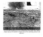
- Figs. 6 to 9 inclusive are photographs of cut material cross-sections.
-
- The invention is based upon use of a laser beam for singulation, as shown in Fig. 1. The process uses an ultraviolet laser to "saw" the package. The laser creates excellent quality cuts which generate only vapor debris, use no consumables, and do not cause any chips or micro-cracks in the cut edges.
- The concept of photo-ablative decomposition of materials using ultraviolet laser pulses was introduced by Srinivasan in 1982. (R. Srinivasan et al.,. Applied physics letters, 41, page 576, 1982). The basic mechanism for material removal differs from longer wavelength processes in that the energy of individual photons at ultra-violet wavelengths is close to the energy of the bonds that hold the material together. Examples of the covalent bond strengths of some representative bonds are shown in Table 1. In addition, at room temperature, the width of the absorption bands is sufficient that, at least for organic covalent bonds, pulsed ultraviolet radiation in the wavelength range below 400nm (>3eV) is sufficient to cause photo-ablative decomposition.
Covalent bond strength in polyatomic organic compounds (Source: handbook of chemistry and physics page F239, Ed. 1978-1979, CRC press). The corresponding wavelength of a photon with this energy is also shown. Bond type eV λ H3C-CH3 3.83 324 H-CH3 4.53 274 CH3CO-COCH3 2.93 423 C6H5CH2-N(CH3)2 2.66 466 F-CH3 4.70 264 - From our investigations into photo-ablative decomposition the following conclusions may be drawn:
- Below a certain threshold of fluence or intensity, no ablation is observed. However, photo-degradation can occur and lead to morphological changes on the material surface. (P.E.Dyer et al., Journal of applied physics, 57, p1420, 1985 ; J.H. Brannon et al., Journal of applied physics, 58, p2036, 1985; R. Srinivasan et al., Applied physics 61 p372, 1987)
- The fragments coming off the surface that is being ablated consist of small clusters of material and gaseous products. (R.C.Estler et al, Applied physics letters, 49, p1175, 1986; G. Koren et al, Applied physics letters, 44, p1112, 1984; G.S. Hansen et al., Journal of applied physics, p1878, 1990.)
- With the exception of 308nm ablation of polyimide (D.L. Singleton et al., Chemical physics, 144, p415, 1990), the laser pulse duration and shape are reported to have a determinant effect on the ablation.(R. Srinivasan et al, Applied physics letters, 53,p 1233, 1988.)
- The photo-ablation process generally occurs on a fast time-scale less than the laser pulse width of 20ns.
- A blast wave is generated following pulse impact and absorption. (R. Srinivasan et al, Journal of applied physics, 68, p1842, 1990).
- Absorption coefficient is defined at low power density (mW/cm2) and etch rate represents material removal at much higher power densities (mW to MW/cm2). As ablation starts with absorption, there is often a link between absorption coefficient, alpha, and the etch depth. That is, a strong absorber will have a lower ablation threshold (power density) than a weak absorber. However, etch rate for a strong absorber can be much smaller as most of the photonic energy is confined to shallower depths. This is a common observation. However, this is by no means the general case. Absorption is only a necessary condition. It is not sufficient. A high absorber could relax radiatively or thermally to its original ground state. To have photo-ablation requires bond breaking. i.e. a reaction from reactant to products via excited state (photo-chemical reaction) or ground state (photo-thermal reaction). Secondly, because of the different intensity regime between the spectroscopic measurement of alpha and the ablation regime, non-linear phenomena such as multi-photon absorption could lead to a dramatic increase (and then possibly to saturation) of the etch rate with power density. In this way, two materials having a similar alpha (i.e. at low intensity) but completely different etch rates (at high intensity) because, in one material, two-photon or multi-photon absorption sets in. For example, at 355nm the aromatic rings of organic are not yet excited (absorption peaks at 240-280nm). But with sufficient power -photon bond breaking may occur.
- A true description of the processes is difficult because (i) most of the cross sections and relaxation times are unknown, and (ii) ablation happens in the solid state where multi-molecular events, (i.e. the way the energy of the broken bonds dissipates into the matrix), mechanical properties, and thermal properties are also of importance.
- The apparatus of the invention uses an ultra-violet solid state laser to cut materials that form chip scale packages such as ball grid arrays, circuit board materials and other "thin film" type materials that may form the lamellae of such laminated packages.
- Solid state YAG/YLF and NVO4 lasers and other lasers operating with fundamental laser emission in the visible or infra red may be converted to ultraviolet lasers through second and third harmonic generation, sum and difference frequency mixing in second order nonlinear crystals.
- As an example, using lasers operating in the "third harmonic" regime we have established that with average power in excess of 3W, we can meet or better the cut rate required to match most BGA process line throughputs.
- The apparatus consists of an ultraviolet laser system as described above, and a beam positioning mechanism. The beam positioning mechanism may be a multiple axis stage as illustrated in Fig. 2 or a scanning galvanometer as illustrated in Fig. 3.
- Referring to Fig. 2 a beam positioning mechanism 30 is illustrated. A frame 31 supports a target 32 to be singulated. The optical path is:-
- 33: laser beam source,
- 34: beam optics (expander),
- 35: fixed mirror,
- 36: fixed mirror,
- 37: mirror movable in X direction,
- 38: mirror movable in Y direction,
- 39: camera for alignment to package features, and
- 40: a focusing lens.
-
- The advantages of the translational stage approach are:
- Small spot sizes are possible over a large area
- Variation in spot size may be effectively eliminated by mirror control.
- Highly repeatable and accurate positioning
- The cut process may be monitored in real time by observing the light energy reflected from the surface of the material being cut back-reflected along the path of the incident beam and on to a photo-electric detector. In the event that the material has been completely cut, there will be no reflective surface and the signal at the detector will drop to a background level, ideally zero. The reflected light may be U.V. laser light, in which case a beam splitter for the laser wavelength is used. In another embodiment a mirror transparent to Ultraviolet (e.g. 355nm) is used to reflect a second wavelength such as the second harmonic wavelength (e.g. 532nm). In this instance, there is no input power sacrifice at the ultraviolet wavelength.
- Another possibility is that the feedback mechanism is the visible to infrared emission of the plume generated during the cutting process. In the absence of this plume, no cutting occurs and the sample has been cut through. The presence of the plume may be taken as evidence that cutting is occurring. Furthermore, the spectral content of the plume provides information on the material that is being cut.
- Real time control of cutting multi-layer materials is possible by monitoring the spectral output at each position of the pulse on the cut scan. From the control point, once the signal can be delivered and processed before the next measurement occurs it is possible to control the laser output parameters on a pulse to pulse basis. This is beneficial in the case where composite materials such as laminated packages may have variations in material distribution across the cut surface. In addition, once a layer has been completely cut through the laser parameters can be varied on the fly such that the cut process is optimised for the next layer.
- A second option for beam delivery and position control is to use a scanning galvanometer. Fig. 3 shows the essential geometry. Two mirrors are mounted on current driven galvanometer coils that rotate the axes on which the mirror is mounted. Scanning from position A to position D can be achieved by scanning galvanometer Galv.1 through an angle G1 with galvanometer Galv.2 oriented so that its mirror reflects along this line. Scanning from position A to position B may be achieved by rotating galvanometer Galv.2 through an angle G2 with galvanometer Galv.1 fixed for position A on the AD line. Accordingly, any position in two dimensions may be marked out by a combination of moves of the two mirrors. The galvanometer approach allows high acceleration and deceleration times, resulting in minimal time between moves and minimal effect on processing time.
- To deliver a focussed laser beam to the work surface it is necessary to use a flat field lens or a z-axis focus adjustment. Both galvanometer and gantry systems are possible for ultraviolet laser excising of circuit board and chip scale package materials. The choice depends on the exact requirements of the cutting process.
- In a situation where the high acceleration of a galvanometer approach is required with high accuracy a combination of a galvanometer and XY stage or gantry approach can provide this. For example, a specimen may be mounted on an XY stage below a galvanometer arrangement. High speed and acceleration is possible over a small area with a high degree of accuracy through the galvo action and slower moves with high accuracy are possible with the XY stage. Where the number of slower moves is low, the overall effect on processing time will be negligible. This galvo/XY stage combination allows accuracy and speed to be exploited.
- The type of laser, the laser output specifications, the beam delivery method and the material that is to be cut all affect the rate at which the material is cut and the quality of the resulting cut.
- The optical configuration described above delivers a laser beam to the surface to be cut. Using a lens, the beam is focussed to a small diameter, high-intensity spot. The laser fires pulses in sequence at rates greater than 1 kHz. Cutting is achieved by scanning the beam over the sample (or scanning the sample through the beam) at a speed such that there is sufficient overlap between the pulses to allow cutting. We have established that in order to maximise the cut speed and quality it is necessary to ensure the correct overlap factor and to use multiple passes over the same path to cut through a material. From our investigations into the cutting process we have established that:
- The laser, material and scanning parameters form a set of parameters that must be optimised for the optimum cut speed and quality.
- Using the average power, repetition rate, and scan rate relationships it is possible to ensure a linear scaling of cut rate with average power by using multiple passes.
- The cut quality is also affected by the overlap.
- The focal spot size may be reduced or increased and the corresponding overlap parameter adjusted (by adjusting rep rate or scan rate) if higher peak power density is required.
- The high power density (> 100MW/cm2) scaling laws for etch rate or cut rate are different to those observed for low power (1KW to 100MW/cm2)
- Wavelength of the laser beam.
Pulse energy: The pulse energy is the energy within a single pulse of the pulse train, and the energy density is the value per cm2.
Repetition frequency defines the number of pulses per second. - Scan speed: The scan speed of the laser relative to the sample is defined by the required spatial overlap for a given spot size at a fixed repetition rate.
- Overlap: The overlap is defined as the percentage of the beam diameter that overlaps spatially with the other pulses in sequence.
- Spot size: The spot size or beam diameter determines the peak power density(W/cm2) and fluence (J/cm2) at the cutting surface. Also, the spot size determines at which velocity the laser should be scanned relative to the sample to achieve the required overlap.

- Average power is the pulse energy delivered by all pulses in one second. Energy x Repetition frequency.
- Pulse width: Pulse width determines the peak power and the peak power density
- Peak power density is the peak power delivered per unit area (cm2).
- The linear absorption coefficient, α, determines the penetration depth of the pulse. The Beer Lambert law states that
- Accordingly, the depth at which the incident intensity, I0, reduces by 50% (I=I0/2) is given by
- Two-photon absorption may be understood by taking the total absorption as the sum of a linear and intensity dependent absorption coefficient given by
- For a fixed intensity wave and at a wavelength where two-photon absorption occurs the resulting decrease in the wave intensity may be represented mathematically bywhere I0 is the initial intensity of the wave. If there is negligible two-photon absorption, α2 is zero and this expression reduces to the Beer-Lambert law for linear absorption. In the presence of two-photon absorption an intensity limiting effect occurs.

- Considering these expressions the following conclusions may be drawn.
- Energy may be absorbed even if the low intensity absorption coefficient is zero. (A)
- As the intensity is increased the total energy absorbed increases (A)
- As Intensity is increased in the presence of two photon absorption, the depth at which the intensity is above a threshold value, Ith, increases also.
- Similar to two photon absorption three and multi-photon absorption can be defined using the procedures above.
- Other nonlinear absorption processes include absorption saturation, inverse saturable absorption, and photo-ionisation.
- Using an assist gas it is possible to ensure that debris is not redepositied on the sample surface. Also, some gases may enhance photo- removal of material and others may suppress unwanted non-clean chemical processes.
- Based on the parameter space described it is possible to state the following.
- The wavelength should be less than 400nm.
- The minimum energy density should be 100J/cm2 or the minimum peak power density should be 1.0GW/cm2.
- For a given laser pulse energy, the scan rate and repetition rate define overlap. By increasing scan rate and repetition rate the overlap can be maintained, the number of scans remains constant but the time required to cut decreases linearly according to the increase in scan rate. i.e. the cut rate decreases linearly.
- For a given pulse repetition frequency, scan speed and overlap (5% - 95%), the number of passes required to cut through a sample decreases as the energy of the pulse is increased. For UV solid state lasers with average power up to 4W working at the optimum cut rate and with parameters set to achieve this, the increase generally follows a linear trend. As well as standard photo-ablation, nonlinear absorption and ionization effects occur in the higher power density regime (greater than 100MW/cm2).
- Accordingly, the cut rate increases with a linear or better than linear dependence on pulse energy. For the UV lasers described above, it is possible to reduce the number of scans required to achieve cutting by:
- optimising the cut rate at a low power of 3 W, and
- by scaling the average power output upward such that the only parameter to change is the pulse energy (for example yielding 15W average power),.
- Depending on the material it may be possible to reduce the number of scans by five (15W/3W, linear), more than five (super-linear) or less than five (saturating) to achieve complete cutting. Generally, for the materials in chip scale packages, circuit boards and flex circuits, the cut rate increases linearly or "super" linearly as pulse energy is increased.
- As example of the scaling laws above consider a 1 mm thick multi-layer structure. We achieve a cut rate of 4.2 mm/s with an average power of 3W. This is achieved with a repetition rate of 5.5 kHz, pulse-width of 95ns, scanning at 100mm/s and with a 25micron spot size. This requires a total of 24 passes to cut through and achieve the quality required. For this example the corresponding energy density (or fluence) and peak power density may be calculated as:
- Increasing the scan rate to 300mm/s and increasing the repetition rate to 16.5 kHz, and taking the same pulse energy, it is possible to achieve a cut rate of at least 12.6mm/s. This requires an average power of 9W. This is within the capability of diode pumped UV solid state lasers.
- Increasing the power further at this repetition rate (for example to 18W) and maintaining all other parameters can then result in a doubling of this rate to 25.2mm/s.
- Keeping all of the above parameters the same, further improvements ( cut rate increases) are possible by reducing the pulse-width. Reducing pulse-width for a fixed energy results in an increase in peak power. Nonlinear processes are strongly dependent on peak power and where there is a nonlinear absorption, ionization, or refraction process contributing to the rate of material removal, reducing the pulse-width will increase the material removal rate resulting in an increased cut rate. Ablation also shows a strong pulse width dependence.
- A further parameter that affects the beam energy/power density at the sample is the beam diameter. Focussing to a smaller beam waist at the sample results in an increase in the peak power density, average power density and energy density at the sample. All of these result in an increase in material removal. Eventually, however, the "kerf" or width of the cutting region physically occludes material removal and it is necessary to ensure a sufficient kerf width to maintain the material removal rate. A second factor which must be taken into account is the depth of field. Focussing too tightly will reduce the depth of field. Finally, reproducibility of the positioning system will become critical at smaller beam sizes. With these factors in mind, the optimum beam diameter lies in the range from 8 to 70 microns.
- The parameter space is then defined by (in no particular order):
- Pulsewidth : < 100ns
- Beam waist : < 70 microns
- Average power : >3W
- Repetition frequency: > 1kHz
- Number of passes: > 1
- Wavelength : < 400nm
- Overlap ( rep rate and scan rate dependent): 5% to 95%, and preferably 30% to 50%. Minimum energy density of 100J/cm2 or a minimum peak power density of 1.0GW/cm2.
-
- The laser was a frequency tripled Q-switched Nd: Yag laser. The laser stability was better than 7% about the mean and the mode operation was in the fundamental TEM00. The operating specification is shown in Table 2.
Laser parameters for Example 1. Parameter Value Wavelength 355nm Average power 4W Pulse-width 95 ns Rep Rate 5.5kHz Pulse energy 0.727mJ Fluence 148 J/cm2 Peak Power 7.7KW Peak Power density 1.56 GW/cm2 - The cutting parameters for five representative flex circuit materials were used. The samples consist of solder mask, poly-imide and adhesive in various laminations.
- Sample #1: Contains 5 layers of material. 2-poly-imide, 2-adhesive, 1- solder mask. Sample #1A: Sample is identical to sample # 1 except for the continuation of the solder mask over the heat bond area on one side.
- Sample #2: Sample contains 3 layers of material. 1-poly-imide, 2-solder mask.
- Sample #3: Sample contains 5 layers in the non-copper loaded areas. 3-poly-imide, 2-adhesive
- Sample #4: Sample contains 3 layers of material(1-liquid crystal polymer, 2-solder mask
- The optimum rep rate was established by varying the rep rate and scan speed, ensuring similar overlap and counting the number of passes required to machine through. Although the rep rate could be tuned up to 15kHz the optimum machining performance is obtained when the average power is near the peak. At this point the individual pulse energy may not be at a maximum but the total delivered energy is such that that cutting occurs in the fastest possible time.
- The conclusion that may be drawn from the graphs in Figs. 4 and 5 is:
- Above a power density of 0.5 GW/cm2, by varying the pulse energy only, the cut rate increases without saturation. This relationship varies slightly depending on the sample type and thickness but the relationship may be defined as linearly proportional or better.
- Using the same laser operating parameters as in Example 1 the cut rate for a 1mm thick overmolded BGA package was measured as 4.2mm /sec at 3W average power. This was accomplished by using 24 passes at a speed of 100mm/s ( approx. 50% overlap at the FWHM intensity point). 20X and 100X SEM images of the edges obtained are shown in Figs. 6 and 7 respectively. The sample consists of solder mask, glass fiber matrix, epoxy and adhesive, copper and encapsulant regions. It is clear that the edge quality is defect free. The open space that appears is likely due to the free volume of the encapsulant material.
- The experiment was repeated with two passes and scanning with a speed of 8.3mm/sec. This corresponds to a 93% overlap for a 25 micron spot. The 20X and 100X SEM images of the edge are shown in Figs. 8 and 9 respectively. It is very clear that the cut quality is not as good as in the case for 50% overlap and that this is an important factor in achieving the required cut quality.
- The following example indicates the laser beam power requirements. 1mm thick multilayer overmolded BGA package (see Example 2).
- Average power used = 3W
- Repetition frequency 5.5kHz
- Spot size 25 microns (1/e2)
- Scan speed 100mm/s
- Number of passes required to cut through = 24
- Effective cut rate = 4.2mm/second
-
- Depth of focus:Where ω(z) is the beam waist at a distance z from the minimum beam waist at ω0 and λ is the wavelength. Allowing 5% spot size variation, i.e. ω(z)=1.05 ω0
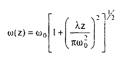
- With ω0 = 25 microns and at a wavelength of 355nm and solve for z=Δz
- Form this data we can conclude that the energy density, peak power density and average power density regime is unique and also that the depth of focus over which this regime can exist yields a completely new set of parameters for laser machining using Ultraviolet light.
- Using a laser of this type with an average power greater than 3W yields a completely new regime of power densities which may be applied to the efficient machining of multiple layer and composite materials such as those used in electronic manufacturing.
- It will be appreciated from the above that the invention achieves the following advantages over the prior art.
-
- Parts transferred directly from previous process in panel, strip, or boats
- For example, for singulation of a package having a thickness of lmm, a speed of greater than 1000UPH (units per hour) is achieved with a 5W laser. This may be greater with more power.
- No cleaning is required
- Unlike use of a diamond saw, the laser cutting process does not incur costs associated with wafer saw, for UV tape deionised water, drying, and for saw consumables.
- Laser excising consumes less space in class 1000 clean room area. Laser excising and inspection require only approximately 2 square metre, as opposed to approximately 5 square metres for prior art sawing, handling, and inspection equipment.
- The excising method of the invention results in much smaller "kerf". Typically in the prior art methods saws are given 250µm waste area and use 175um cuts. In the invention, the waste area is 25µm or less. Thus, the invention achieves greater "real estate" for components, particularly small components. Also, the invention achieves edges with less stress and no micro-cracking.
- The invention is not limited to the embodiments described but may be varied in construction and detail within the scope of the claims.
Claims (34)
- A method for singulating plural electronic circuits (2, 6, 21) by cutting material joining the circuits, the method comprising the steps of:generating a pulsed laser beam having the following properties:a wavelength of less than 400nm, anda minimum energy density of 100 J/cm2 or a minimum peak power density of 1GW/cm2;aligning the beam relative to a feature or fiducial of the material to be cut; and applying the beam to the material until a cut has been made.
- A method as claimed in claim 1, wherein the step of applying the beam comprises moving the beam to have a spatial overlap of consecutive pulses, the overlap being in the range of 5% to 95%.
- A method as claimed in claim 2, wherein the overlap is in the range of 30% to 50%.
- A method as claimed in any of the preceding claims, wherein the step of applying the beam comprises moving the beam in a plurality of passes over the material.
- A method as claimed in claim 4, wherein the beam is moved in more than five passes.
- A method as claimed in any preceding claim, wherein the step of generating a laser beam comprises generating a laser beam with a pulse repetition rate of greater than 1kHz.
- A method as claimed in any preceding claim, wherein the step of generating a laser beam comprises generating a laser beam with a depth of focus at least equal to a thickness of the material to be cut.
- A method as claimed in any of the preceding claims wherein said material is a semiconductor.
- A method as claimed in any of the preceding claims arranged to singulate an electronic integrated circuit.
- A method as claimed in any of the preceding claims wherein said material is a laminate material.
- A method as claimed in claim 10, wherein the laminate material contains two or more layers selected from BT epoxy, glass fibers, copper, gold, poly-imide, adhesive, overmold materials, underfills, conductors, dielectrics, stiffeners, stabilisers, protectors or other materials as used in electronic packaging.
- A method as claimed in claims 10 or 11, wherein individual layers of the laminate material have different ablation and ionization thresholds, different ablation and ionization rates, and different non-linear absorption and non-ionization coefficients.
- A method as claimed in any of the preceding claims, wherein the step of generating the laser beam comprises the additional step of obtaining optical feedback from the material being cut and varying parameters of the laser beam dependent on the optical feedback.
- A method as claimed in claim 13, wherein the step of obtaining optical feedback comprises detecting whether light is reflected from a surface of the material being cut to determine when the material has been cut through.
- A method as claimed in claims 13 or 14, wherein the step of obtaining optical feedback comprises detecting optical emissions from a plume generated by the cutting process.
- A method as claimed in claim 15, wherein the step of obtaining optical feedback comprises determining a spectral content of the plume to provide information on the material being cut.
- A method as claimed in any of claims 13 to 16, wherein the step of varying parameters of the laser beam comprises varying parameters between successive passes.
- A method as claimed in any of claims 13 to16, wherein the step of varying parameters of the laser beam comprises varying parameters between successive pulses during a pass.
- A method as claimed in any preceding claim, wherein the beam is generated from a solid state laser with a characteristic average power peak at a specific repetition frequency.
- A method as claimed in any preceding claim, wherein the beam is controlled so that the average power drops as the repetition frequency is increased or decreased, and although individual pulse energy may be increased at a repetition frequency other than the repetition frequency for maximum average power the maximum cut rate is achieved at a repetition frequency other than either of these frequencies due to the contribution of other laser cutting parameters.
- A method as claimed in any preceding claim, wherein the average power of said laser beam is greater than 3W, with a pulse width less than 100 nanoseconds, a consecutive pulse spatial overlap of 10-70%, and a beam diameter less than 70 microns at the 1/e2 point of a spatial intensity profile.
- A method as claimed in any preceding claim, wherein the laser beam is generated by a diode laser pumped gain medium device with a fundamental emission in a 900 to 1600nm wavelength range and with second, third, fourth or fifth harmonic generation of ½, 1/3, ¼, 1/5 of this wavelength which is obtained by placing appropriate crystals in the laser cavity or outside the laser cavity.
- A method as claimed in claim 22, wherein said laser device is one of a Nd:YAG, Nd:YLF, Nd:YVO4 or other combination of Impurity:Host gain media lasing in the required range and with harmonic generation to an operating wavelength of less than 400nm.
- A method as claimed in any preceding claim, wherein the beam is delivered to a surface of the material to be cut using one or more mirrors mounted on one or more scanning galvanometers, and in which a required spot size is achieved by use of an on-axis lens position adjustment at a stage before the galvanometer mirror, or at a stage after the galvanometer mirror by a lens of a flat field lens, or by the use of a combination of these lenses.
- A method as claimed in any of claims 1 to 23, wherein the laser beam is delivered using one or more mirrors mounted on one or more translational stages, and focusing is achieved by the use of a telescope or an on-axis lens before the moving mirrors or lens mounted before the material surface and moving with the beam delivery mirror such that the focussed beam is delivered to the material surface.
- A method as claimed in any of claims 1 to 23, wherein the beam is telescoped and focussed to achieve the required spot size at the material to be cut with a telescope or scan lens chosen such that a waist of the beam remains within a specified percentage of an optimum spot size throughout the range over which the beam is delivered, and wherein the range is greater than the thickness of the material to be cut.
- A method as claimed in any preceding claim, wherein an assist gas is used to assist the cutting process by preventing debris from being deposited on the material surface, and wherein the assist gas removes material generated during the cutting process so that the debris does not create absorption or scattering of consecutive laser light pulses.
- A method as claimed in claim 27, wherein the assist gas is used to provide an inert atmosphere to prevent unwanted specific photochemical or photo-physical reactions from occurring during cutting.
- A method as claimed in any preceding claim, wherein a vacuum suction process is provided to extract fumes and solid debris generated at the cut surface.
- A method as claimed in any preceding claim, wherein the step of aligning the beam relative to a feature or fiducial of the material comprises using a sensor and means for image processing to provide coordinates along which cutting occurs, and wherein a beam positioning mechanism is controlled to ensure that the laser beam follows a required cutting path.
- A circuit singulation system comprising:means (31) for supporting a plurality of electronic circuits (2,6,21) interconnected by material; a laser beam source (33) comprising means (34) for generating a laser beam having:a wavelength of less than 400nm, anda minimum energy density of 100J/cm2 or a minimum peak power density of 1GW/cm2a beam positioning mechanism comprising means (35-38, 40) for directing the beam at the material and for training the beam along cut lines to singulate at least one of the plurality of electronic circuits.
- A circuit singulation system as claimed in claim 31, wherein the beam positioning mechanism comprises a series of mirrors (35-38) at least some of which are movable for directing the laser beam, and a focusing lens (40).
- A circuit singulation system as claimed in claim 32, wherein the mirrors are linearly movable.
- A circuit singulation system as claimed in claim 32, wherein the mirrors are rotatable.
Applications Claiming Priority (3)
| Application Number | Priority Date | Filing Date | Title |
|---|---|---|---|
| IE990664 | 1999-08-03 | ||
| IE990664 | 1999-08-03 | ||
| PCT/IE2000/000095 WO2001010177A1 (en) | 1999-08-03 | 2000-08-03 | A circuit singulation system and method |
Publications (2)
| Publication Number | Publication Date |
|---|---|
| EP1201108A1 EP1201108A1 (en) | 2002-05-02 |
| EP1201108B1 true EP1201108B1 (en) | 2003-10-22 |
Family
ID=11042109
Family Applications (1)
| Application Number | Title | Priority Date | Filing Date |
|---|---|---|---|
| EP00948225A Expired - Lifetime EP1201108B1 (en) | 1999-08-03 | 2000-08-03 | A circuit singulation system and method |
Country Status (8)
| Country | Link |
|---|---|
| US (1) | US6781093B2 (en) |
| EP (1) | EP1201108B1 (en) |
| JP (2) | JP2003506216A (en) |
| AT (1) | ATE252816T1 (en) |
| AU (1) | AU6178200A (en) |
| DE (1) | DE60006127T2 (en) |
| IE (1) | IE20000618A1 (en) |
| WO (1) | WO2001010177A1 (en) |
Families Citing this family (43)
| Publication number | Priority date | Publication date | Assignee | Title |
|---|---|---|---|---|
| US20020056347A1 (en) * | 2000-11-15 | 2002-05-16 | Signey Ferdinand S. | Method and system for cutting integrated circuit packages |
| NL1016701C2 (en) * | 2000-11-24 | 2002-05-27 | Fico Bv | Method and device for removing a carrier part from a flat carrier. |
| JP2003037085A (en) | 2001-07-06 | 2003-02-07 | Data Storage Inst | Substrate cutting method and apparatus using laser irradiation |
| US7357486B2 (en) | 2001-12-20 | 2008-04-15 | Hewlett-Packard Development Company, L.P. | Method of laser machining a fluid slot |
| US6969822B2 (en) | 2003-05-13 | 2005-11-29 | Hewlett-Packard Development Company, L.P. | Laser micromachining systems |
| US7754999B2 (en) | 2003-05-13 | 2010-07-13 | Hewlett-Packard Development Company, L.P. | Laser micromachining and methods of same |
| JP2005252196A (en) * | 2004-03-08 | 2005-09-15 | Toshiba Corp | Semiconductor device and manufacturing method thereof |
| US6972244B1 (en) * | 2004-04-23 | 2005-12-06 | National Semiconductor Corporation | Marking semiconductor devices through a mount tape |
| US20060097430A1 (en) * | 2004-11-05 | 2006-05-11 | Li Xiaochun | UV pulsed laser machining apparatus and method |
| NL1028588C2 (en) * | 2005-03-22 | 2006-09-25 | Fico Bv | Method and device for separating products with a controlled cut edge and separated product. |
| NL2000028C2 (en) * | 2006-03-16 | 2007-09-18 | Fico Bv | Device for automated laser cutting of a flat carrier provided with encapsulated electronic components. |
| NL2000039C2 (en) * | 2006-03-28 | 2007-10-01 | Fico Bv | Method and device for shielding encapsulated electronic components during laser cutting. |
| US20080067160A1 (en) * | 2006-09-14 | 2008-03-20 | Jouni Suutarinen | Systems and methods for laser cutting of materials |
| GB2458475B (en) * | 2008-03-18 | 2011-10-26 | Xsil Technology Ltd | Processing of multilayer semiconductor wafers |
| KR101605037B1 (en) * | 2010-01-15 | 2016-04-01 | 동우 화인켐 주식회사 | The cutting method of the polarizing plate |
| KR101605034B1 (en) * | 2010-01-15 | 2016-04-01 | 동우 화인켐 주식회사 | The cutting method of the polarizing plate |
| US8361828B1 (en) * | 2011-08-31 | 2013-01-29 | Alta Devices, Inc. | Aligned frontside backside laser dicing of semiconductor films |
| US8399281B1 (en) * | 2011-08-31 | 2013-03-19 | Alta Devices, Inc. | Two beam backside laser dicing of semiconductor films |
| WO2013043434A2 (en) * | 2011-09-20 | 2013-03-28 | 3M Innovative Properties Company | A method, system for manufacturing a circuit board, and the circuit board thereof |
| US9412702B2 (en) * | 2013-03-14 | 2016-08-09 | Intel Corporation | Laser die backside film removal for integrated circuit (IC) packaging |
| US9914985B2 (en) * | 2014-09-09 | 2018-03-13 | G.C. Laser Systems, Inc. | Laser ablation and processing methods and systems |
| CN107205318B (en) * | 2016-03-17 | 2021-01-29 | 塔工程有限公司 | Scribing apparatus and scribing method |
| CN106404786A (en) * | 2016-11-04 | 2017-02-15 | 中国科学院长春光学精密机械与物理研究所 | Circuit board image scanning device |
| KR102437366B1 (en) * | 2017-02-09 | 2022-08-29 | 유에스 신써틱 코포레이션 | Energy machined polycrystalline diamond compacts and related methods |
| KR102629386B1 (en) * | 2017-11-27 | 2024-01-29 | 닛토덴코 가부시키가이샤 | Laser processing method and plastic film of plastic film |
| CN110178228A (en) * | 2017-12-19 | 2019-08-27 | 君泰创新(北京)科技有限公司 | Membrane removal treatment method and equipment |
| CN109635467B (en) * | 2018-12-18 | 2020-12-04 | 深圳市华星光电半导体显示技术有限公司 | Method for acquiring cutting rate of printed circuit board |
| US11342256B2 (en) | 2019-01-24 | 2022-05-24 | Applied Materials, Inc. | Method of fine redistribution interconnect formation for advanced packaging applications |
| IT201900006740A1 (en) * | 2019-05-10 | 2020-11-10 | Applied Materials Inc | SUBSTRATE STRUCTURING PROCEDURES |
| IT201900006736A1 (en) | 2019-05-10 | 2020-11-10 | Applied Materials Inc | PACKAGE MANUFACTURING PROCEDURES |
| US11931855B2 (en) | 2019-06-17 | 2024-03-19 | Applied Materials, Inc. | Planarization methods for packaging substrates |
| PL430653A1 (en) * | 2019-07-18 | 2021-01-25 | Gryglicki Rafał Phu Kontakt | Method of cutting a pieces from polypropylene film and a device for implementing the method |
| US11862546B2 (en) | 2019-11-27 | 2024-01-02 | Applied Materials, Inc. | Package core assembly and fabrication methods |
| CN111001948A (en) * | 2019-12-17 | 2020-04-14 | 广州京海科技有限公司 | A high-efficient type laser cutting equipment for aluminum alloy plate processing |
| US11257790B2 (en) | 2020-03-10 | 2022-02-22 | Applied Materials, Inc. | High connectivity device stacking |
| US11454884B2 (en) | 2020-04-15 | 2022-09-27 | Applied Materials, Inc. | Fluoropolymer stamp fabrication method |
| US11400545B2 (en) | 2020-05-11 | 2022-08-02 | Applied Materials, Inc. | Laser ablation for package fabrication |
| US11232951B1 (en) | 2020-07-14 | 2022-01-25 | Applied Materials, Inc. | Method and apparatus for laser drilling blind vias |
| US11676832B2 (en) | 2020-07-24 | 2023-06-13 | Applied Materials, Inc. | Laser ablation system for package fabrication |
| US11521937B2 (en) | 2020-11-16 | 2022-12-06 | Applied Materials, Inc. | Package structures with built-in EMI shielding |
| US11404318B2 (en) | 2020-11-20 | 2022-08-02 | Applied Materials, Inc. | Methods of forming through-silicon vias in substrates for advanced packaging |
| US11705365B2 (en) | 2021-05-18 | 2023-07-18 | Applied Materials, Inc. | Methods of micro-via formation for advanced packaging |
| US12183684B2 (en) | 2021-10-26 | 2024-12-31 | Applied Materials, Inc. | Semiconductor device packaging methods |
Family Cites Families (24)
| Publication number | Priority date | Publication date | Assignee | Title |
|---|---|---|---|---|
| JPH0466287A (en) * | 1990-07-03 | 1992-03-02 | Sharp Corp | Manufacture of electrical circuit device |
| JPH0785509B2 (en) * | 1990-10-15 | 1995-09-13 | 日本メクトロン株式会社 | Flexible circuit board with carrier tape and manufacturing method thereof |
| JPH04333299A (en) * | 1991-05-08 | 1992-11-20 | Toshiba Corp | Cutting method of film board |
| JPH06142971A (en) * | 1992-11-05 | 1994-05-24 | Ishikawajima Harima Heavy Ind Co Ltd | Underwater processing equipment using ultraviolet pulsed laser light |
| US5500505A (en) * | 1994-05-09 | 1996-03-19 | General Electric Company | Method for cutting epoxy/carbon fiber composite with lasers |
| US5593606A (en) * | 1994-07-18 | 1997-01-14 | Electro Scientific Industries, Inc. | Ultraviolet laser system and method for forming vias in multi-layered targets |
| JP3483969B2 (en) * | 1995-01-27 | 2004-01-06 | 株式会社東芝 | Laser repair method and apparatus for liquid crystal display, and manufacturing method of active matrix type liquid crystal display |
| JPH09219482A (en) * | 1996-02-08 | 1997-08-19 | Hitachi Constr Mach Co Ltd | Positioning device for semiconductor device and dam bar cutting device |
| JP2866831B2 (en) * | 1996-08-30 | 1999-03-08 | 株式会社アドバンテスト | Laser processing equipment positioning method |
| JP3023320B2 (en) * | 1996-12-27 | 2000-03-21 | イビデン株式会社 | Laser processing apparatus, multilayer printed wiring board manufacturing apparatus and manufacturing method |
| WO1998022252A1 (en) | 1996-11-20 | 1998-05-28 | Ibiden Co., Ltd. | Laser machining apparatus, and apparatus and method for manufacturing a multilayered printed wiring board |
| JPH10225788A (en) * | 1997-02-14 | 1998-08-25 | Koike Sanso Kogyo Co Ltd | Laser cutting method and laser cutting torch |
| JP3233060B2 (en) * | 1997-02-26 | 2001-11-26 | 株式会社デンソー | Laser processing method for resin products |
| JPH10277747A (en) * | 1997-04-08 | 1998-10-20 | Toshiba Corp | Processing method and processing apparatus for workpiece |
| US5928526A (en) * | 1997-04-29 | 1999-07-27 | Stellex Microwave Systems, Inc. | Method for manufacturing a substrate having an irregular shape |
| TW411309B (en) * | 1997-05-13 | 2000-11-11 | Taltec Systems Inc | Apparatus and method for automatically separating a silicon chip from a film strip, and apparatus and method of separating chip scale packages from a multi-layered film strip. |
| JP3307280B2 (en) * | 1997-06-05 | 2002-07-24 | 株式会社富士電機総合研究所 | Laser processing equipment |
| WO1999003128A2 (en) | 1997-07-09 | 1999-01-21 | Systemation Engineered Products, Inc. | Singulation system for chip-scale packages |
| CN1205051C (en) * | 1997-07-16 | 2005-06-08 | 奥蒂斯电梯公司 | Method and composition for laser marking, and objects marked with the method and composition |
| JP3769942B2 (en) * | 1997-09-02 | 2006-04-26 | セイコーエプソン株式会社 | Laser processing method and apparatus, and circuit forming method and apparatus for non-conductive transparent substrate |
| JPH11104879A (en) * | 1997-10-01 | 1999-04-20 | Nkk Corp | Laser cutting nozzle and laser cutting method |
| JPH11151584A (en) * | 1997-11-17 | 1999-06-08 | Toshiba Corp | Laser processing method and apparatus |
| JP4132164B2 (en) * | 1997-12-26 | 2008-08-13 | 住友重機械工業株式会社 | Laser drilling machine |
| US6472295B1 (en) * | 1999-08-27 | 2002-10-29 | Jmar Research, Inc. | Method and apparatus for laser ablation of a target material |
-
2000
- 2000-08-03 AU AU61782/00A patent/AU6178200A/en not_active Abandoned
- 2000-08-03 AT AT00948225T patent/ATE252816T1/en active
- 2000-08-03 EP EP00948225A patent/EP1201108B1/en not_active Expired - Lifetime
- 2000-08-03 WO PCT/IE2000/000095 patent/WO2001010177A1/en not_active Ceased
- 2000-08-03 DE DE60006127T patent/DE60006127T2/en not_active Expired - Lifetime
- 2000-08-03 JP JP2001513943A patent/JP2003506216A/en active Pending
- 2000-08-03 IE IE20000618A patent/IE20000618A1/en not_active IP Right Cessation
-
2002
- 2002-02-01 US US10/060,414 patent/US6781093B2/en not_active Expired - Lifetime
-
2012
- 2012-12-06 JP JP2012266877A patent/JP2014007375A/en active Pending
Also Published As
| Publication number | Publication date |
|---|---|
| AU6178200A (en) | 2001-02-19 |
| EP1201108A1 (en) | 2002-05-02 |
| JP2003506216A (en) | 2003-02-18 |
| WO2001010177A1 (en) | 2001-02-08 |
| US6781093B2 (en) | 2004-08-24 |
| ATE252816T1 (en) | 2003-11-15 |
| DE60006127T2 (en) | 2004-07-22 |
| JP2014007375A (en) | 2014-01-16 |
| US20040020901A1 (en) | 2004-02-05 |
| IE20000618A1 (en) | 2001-03-07 |
| DE60006127D1 (en) | 2003-11-27 |
Similar Documents
| Publication | Publication Date | Title |
|---|---|---|
| US6781093B2 (en) | Circuit singulation system and method | |
| US7804043B2 (en) | Method and apparatus for dicing of thin and ultra thin semiconductor wafer using ultrafast pulse laser | |
| US6472295B1 (en) | Method and apparatus for laser ablation of a target material | |
| US7179723B2 (en) | Wafer processing method | |
| EP1341638B1 (en) | Laser machining of semiconductor materials | |
| CN1211862C (en) | Substrate film ablation method and equipment thereof | |
| CN100548564C (en) | Laser processing method and semiconductor device | |
| US8415586B2 (en) | Method for increasing throughput of solder mask removal by minimizing the number of cleaning pulses | |
| US20070141810A1 (en) | Wafer dividing method | |
| US20050101108A1 (en) | Semiconductor wafer dividing method | |
| US20090194516A1 (en) | Method and apparatus for via drilling and selective material removal using an ultrafast pulse laser | |
| US20020149136A1 (en) | Ultraviolet laser ablative patterning of microstructures in semiconductors | |
| CN101432853A (en) | Laser processing of workpieces containing low-K dielectric material | |
| JP4634692B2 (en) | Laser processing method | |
| US20060009008A1 (en) | Method for the laser processing of a wafer | |
| US20060091126A1 (en) | Ultraviolet laser ablative patterning of microstructures in semiconductors | |
| JP2007508946A (en) | Laser processing of locally heated target materials | |
| US7919725B2 (en) | Via hole forming method | |
| US20060261051A1 (en) | Synthetic pulse repetition rate processing for dual-headed laser micromachining systems | |
| US20050205540A1 (en) | Laser beam processing machine | |
| Brannon et al. | Excimer laser ablation of polyimide: a 14-year IBM perspective | |
| Pauchard et al. | Advanced micromachining combining nanosecond lasers with water jet-guided laser technology | |
| Müller | Choosing the Right Laser for Microelectronic Packaging Tasks: With numerous laser technologies available for packaging, understanding the processing and cost characteristics of each is essential to optimizing results | |
| Baek et al. | mu-BGA (ball grid array) singulation with a pulsed Nd: YAG laser | |
| Müller et al. | Laser applications in advanced chip packaging |
Legal Events
| Date | Code | Title | Description |
|---|---|---|---|
| PUAI | Public reference made under article 153(3) epc to a published international application that has entered the european phase |
Free format text: ORIGINAL CODE: 0009012 |
|
| 17P | Request for examination filed |
Effective date: 20020202 |
|
| AK | Designated contracting states |
Kind code of ref document: A1 Designated state(s): AT BE CH CY DE DK ES FI FR GB GR IE IT LI LU MC NL PT SE |
|
| AX | Request for extension of the european patent |
Free format text: AL;LT;LV;MK;RO;SI |
|
| GRAH | Despatch of communication of intention to grant a patent |
Free format text: ORIGINAL CODE: EPIDOS IGRA |
|
| GRAS | Grant fee paid |
Free format text: ORIGINAL CODE: EPIDOSNIGR3 |
|
| GRAA | (expected) grant |
Free format text: ORIGINAL CODE: 0009210 |
|
| AK | Designated contracting states |
Kind code of ref document: B1 Designated state(s): AT BE CH CY DE DK ES FI FR GB GR IE IT LI LU MC NL PT SE |
|
| PG25 | Lapsed in a contracting state [announced via postgrant information from national office to epo] |
Ref country code: FI Free format text: LAPSE BECAUSE OF FAILURE TO SUBMIT A TRANSLATION OF THE DESCRIPTION OR TO PAY THE FEE WITHIN THE PRESCRIBED TIME-LIMIT Effective date: 20031022 Ref country code: ES Free format text: LAPSE BECAUSE OF FAILURE TO SUBMIT A TRANSLATION OF THE DESCRIPTION OR TO PAY THE FEE WITHIN THE PRESCRIBED TIME-LIMIT Effective date: 20031022 Ref country code: CY Free format text: LAPSE BECAUSE OF FAILURE TO SUBMIT A TRANSLATION OF THE DESCRIPTION OR TO PAY THE FEE WITHIN THE PRESCRIBED TIME-LIMIT Effective date: 20031022 |
|
| REG | Reference to a national code |
Ref country code: GB Ref legal event code: FG4D |
|
| RIN1 | Information on inventor provided before grant (corrected) |
Inventor name: OWEN, MARK Inventor name: CONLON, PETER Inventor name: BOYLE, ADRIAN Inventor name: MAHON, JAMES |
|
| REG | Reference to a national code |
Ref country code: CH Ref legal event code: EP |
|
| REG | Reference to a national code |
Ref country code: CH Ref legal event code: NV Representative=s name: E. BLUM & CO. PATENTANWAELTE |
|
| REG | Reference to a national code |
Ref country code: IE Ref legal event code: FG4D |
|
| REF | Corresponds to: |
Ref document number: 60006127 Country of ref document: DE Date of ref document: 20031127 Kind code of ref document: P |
|
| RAP2 | Party data changed (patent owner data changed or rights of a patent transferred) |
Owner name: XSIL TECHNOLOGY LIMITED |
|
| PG25 | Lapsed in a contracting state [announced via postgrant information from national office to epo] |
Ref country code: GR Free format text: LAPSE BECAUSE OF FAILURE TO SUBMIT A TRANSLATION OF THE DESCRIPTION OR TO PAY THE FEE WITHIN THE PRESCRIBED TIME-LIMIT Effective date: 20040122 Ref country code: SE Free format text: LAPSE BECAUSE OF FAILURE TO SUBMIT A TRANSLATION OF THE DESCRIPTION OR TO PAY THE FEE WITHIN THE PRESCRIBED TIME-LIMIT Effective date: 20040122 Ref country code: DK Free format text: LAPSE BECAUSE OF FAILURE TO SUBMIT A TRANSLATION OF THE DESCRIPTION OR TO PAY THE FEE WITHIN THE PRESCRIBED TIME-LIMIT Effective date: 20040122 |
|
| NLT2 | Nl: modifications (of names), taken from the european patent patent bulletin |
Owner name: XSIL TECHNOLOGY LIMITED |
|
| LTIE | Lt: invalidation of european patent or patent extension |
Effective date: 20031022 |
|
| ET | Fr: translation filed | ||
| PG25 | Lapsed in a contracting state [announced via postgrant information from national office to epo] |
Ref country code: LU Free format text: LAPSE BECAUSE OF NON-PAYMENT OF DUE FEES Effective date: 20040803 |
|
| PLBI | Opposition filed |
Free format text: ORIGINAL CODE: 0009260 |
|
| PLAX | Notice of opposition and request to file observation + time limit sent |
Free format text: ORIGINAL CODE: EPIDOSNOBS2 |
|
| PG25 | Lapsed in a contracting state [announced via postgrant information from national office to epo] |
Ref country code: MC Free format text: LAPSE BECAUSE OF NON-PAYMENT OF DUE FEES Effective date: 20040831 |
|
| 26 | Opposition filed |
Opponent name: SIEMENS AG CORPORATE TECHNOLOGY - CT IP L&A Effective date: 20040722 |
|
| NLR1 | Nl: opposition has been filed with the epo |
Opponent name: SIEMENS AG CORPORATE TECHNOLOGY - CT IP L&A |
|
| PLBB | Reply of patent proprietor to notice(s) of opposition received |
Free format text: ORIGINAL CODE: EPIDOSNOBS3 |
|
| PLBP | Opposition withdrawn |
Free format text: ORIGINAL CODE: 0009264 |
|
| PLBD | Termination of opposition procedure: decision despatched |
Free format text: ORIGINAL CODE: EPIDOSNOPC1 |
|
| PLBM | Termination of opposition procedure: date of legal effect published |
Free format text: ORIGINAL CODE: 0009276 |
|
| STAA | Information on the status of an ep patent application or granted ep patent |
Free format text: STATUS: OPPOSITION PROCEDURE CLOSED |
|
| 27C | Opposition proceedings terminated |
Effective date: 20070331 |
|
| REG | Reference to a national code |
Ref country code: CH Ref legal event code: PFA Owner name: XSIL TECHNOLOGY LIMITED Free format text: XSIL TECHNOLOGY LIMITED#UNIT 2, TRINITY ENTERPRISE CENTRE, PEARSE STREET#DUBLIN 2 (IE) -TRANSFER TO- XSIL TECHNOLOGY LIMITED#SILVERSTONE HOUSE, BALLYMOSS ROAD#SANDYFORD, DUBLIN 18 (IE) |
|
| NLR2 | Nl: decision of opposition |
Effective date: 20070331 |
|
| REG | Reference to a national code |
Ref country code: CH Ref legal event code: PFA Owner name: XSIL TECHNOLOGY LIMITED Free format text: XSIL TECHNOLOGY LIMITED#SILVERSTONE HOUSE, BALLYMOSS ROAD#SANDYFORD, DUBLIN 18 (IE) -TRANSFER TO- XSIL TECHNOLOGY LIMITED#SILVERSTONE HOUSE, BALLYMOSS ROAD#SANDYFORD, DUBLIN 18 (IE) |
|
| REG | Reference to a national code |
Ref country code: FR Ref legal event code: CA |
|
| PG25 | Lapsed in a contracting state [announced via postgrant information from national office to epo] |
Ref country code: PT Free format text: LAPSE BECAUSE OF NON-PAYMENT OF DUE FEES Effective date: 20040322 |
|
| PLAB | Opposition data, opponent's data or that of the opponent's representative modified |
Free format text: ORIGINAL CODE: 0009299OPPO |
|
| REG | Reference to a national code |
Ref country code: GB Ref legal event code: 732E Free format text: REGISTERED BETWEEN 20090514 AND 20090520 |
|
| REG | Reference to a national code |
Ref country code: CH Ref legal event code: PUE Owner name: ELECTRO SCIENTIFIC INDUSTRIES, INC. Free format text: XSIL TECHNOLOGY LIMITED#SILVERSTONE HOUSE, BALLYMOSS ROAD#SANDYFORD, DUBLIN 18 (IE) -TRANSFER TO- ELECTRO SCIENTIFIC INDUSTRIES, INC.#13900 NW SCIENCE PARK DRIVE#PORTLAND, OR 97229 (US) |
|
| NLS | Nl: assignments of ep-patents |
Owner name: ELECTRO SCIENTIFIC INDUSTRIES, INC. Effective date: 20090814 |
|
| REG | Reference to a national code |
Ref country code: FR Ref legal event code: TP |
|
| REG | Reference to a national code |
Ref country code: FR Ref legal event code: PLFP Year of fee payment: 17 |
|
| PGFP | Annual fee paid to national office [announced via postgrant information from national office to epo] |
Ref country code: NL Payment date: 20160826 Year of fee payment: 17 |
|
| PGFP | Annual fee paid to national office [announced via postgrant information from national office to epo] |
Ref country code: GB Payment date: 20160830 Year of fee payment: 17 Ref country code: CH Payment date: 20160829 Year of fee payment: 17 Ref country code: IT Payment date: 20160824 Year of fee payment: 17 Ref country code: DE Payment date: 20160826 Year of fee payment: 17 Ref country code: IE Payment date: 20160826 Year of fee payment: 17 |
|
| PGFP | Annual fee paid to national office [announced via postgrant information from national office to epo] |
Ref country code: FR Payment date: 20160825 Year of fee payment: 17 |
|
| PGFP | Annual fee paid to national office [announced via postgrant information from national office to epo] |
Ref country code: BE Payment date: 20160829 Year of fee payment: 17 |
|
| PGFP | Annual fee paid to national office [announced via postgrant information from national office to epo] |
Ref country code: AT Payment date: 20170719 Year of fee payment: 18 |
|
| REG | Reference to a national code |
Ref country code: DE Ref legal event code: R119 Ref document number: 60006127 Country of ref document: DE |
|
| REG | Reference to a national code |
Ref country code: CH Ref legal event code: PL |
|
| REG | Reference to a national code |
Ref country code: NL Ref legal event code: MM Effective date: 20170901 |
|
| GBPC | Gb: european patent ceased through non-payment of renewal fee |
Effective date: 20170803 |
|
| PG25 | Lapsed in a contracting state [announced via postgrant information from national office to epo] |
Ref country code: LI Free format text: LAPSE BECAUSE OF NON-PAYMENT OF DUE FEES Effective date: 20170831 Ref country code: CH Free format text: LAPSE BECAUSE OF NON-PAYMENT OF DUE FEES Effective date: 20170831 |
|
| REG | Reference to a national code |
Ref country code: FR Ref legal event code: ST Effective date: 20180430 |
|
| REG | Reference to a national code |
Ref country code: IE Ref legal event code: MM4A |
|
| REG | Reference to a national code |
Ref country code: BE Ref legal event code: MM Effective date: 20170831 |
|
| PG25 | Lapsed in a contracting state [announced via postgrant information from national office to epo] |
Ref country code: NL Free format text: LAPSE BECAUSE OF NON-PAYMENT OF DUE FEES Effective date: 20170901 |
|
| PG25 | Lapsed in a contracting state [announced via postgrant information from national office to epo] |
Ref country code: IE Free format text: LAPSE BECAUSE OF NON-PAYMENT OF DUE FEES Effective date: 20170803 Ref country code: GB Free format text: LAPSE BECAUSE OF NON-PAYMENT OF DUE FEES Effective date: 20170803 Ref country code: DE Free format text: LAPSE BECAUSE OF NON-PAYMENT OF DUE FEES Effective date: 20180301 |
|
| PG25 | Lapsed in a contracting state [announced via postgrant information from national office to epo] |
Ref country code: BE Free format text: LAPSE BECAUSE OF NON-PAYMENT OF DUE FEES Effective date: 20170831 Ref country code: IT Free format text: LAPSE BECAUSE OF NON-PAYMENT OF DUE FEES Effective date: 20170803 Ref country code: FR Free format text: LAPSE BECAUSE OF NON-PAYMENT OF DUE FEES Effective date: 20170831 |
|
| REG | Reference to a national code |
Ref country code: AT Ref legal event code: MM01 Ref document number: 252816 Country of ref document: AT Kind code of ref document: T Effective date: 20180803 |
|
| PG25 | Lapsed in a contracting state [announced via postgrant information from national office to epo] |
Ref country code: AT Free format text: LAPSE BECAUSE OF NON-PAYMENT OF DUE FEES Effective date: 20180803 |