EP1199857A2 - Tri-State-Treiberanordnung - Google Patents
Tri-State-Treiberanordnung Download PDFInfo
- Publication number
- EP1199857A2 EP1199857A2 EP01121602A EP01121602A EP1199857A2 EP 1199857 A2 EP1199857 A2 EP 1199857A2 EP 01121602 A EP01121602 A EP 01121602A EP 01121602 A EP01121602 A EP 01121602A EP 1199857 A2 EP1199857 A2 EP 1199857A2
- Authority
- EP
- European Patent Office
- Prior art keywords
- tri
- state
- output
- driver
- limit
- Prior art date
- Legal status (The legal status is an assumption and is not a legal conclusion. Google has not performed a legal analysis and makes no representation as to the accuracy of the status listed.)
- Granted
Links
Images


Classifications
-
- H—ELECTRICITY
- H03—ELECTRONIC CIRCUITRY
- H03K—PULSE TECHNIQUE
- H03K19/00—Logic circuits, i.e. having at least two inputs acting on one output; Inverting circuits
- H03K19/02—Logic circuits, i.e. having at least two inputs acting on one output; Inverting circuits using specified components
- H03K19/08—Logic circuits, i.e. having at least two inputs acting on one output; Inverting circuits using specified components using semiconductor devices
- H03K19/082—Logic circuits, i.e. having at least two inputs acting on one output; Inverting circuits using specified components using semiconductor devices using bipolar transistors
- H03K19/0823—Multistate logic
- H03K19/0826—Multistate logic one of the states being the high impedance or floating state
-
- H—ELECTRICITY
- H04—ELECTRIC COMMUNICATION TECHNIQUE
- H04L—TRANSMISSION OF DIGITAL INFORMATION, e.g. TELEGRAPHIC COMMUNICATION
- H04L25/00—Baseband systems
- H04L25/02—Details ; arrangements for supplying electrical power along data transmission lines
- H04L25/0264—Arrangements for coupling to transmission lines
- H04L25/0266—Arrangements for providing Galvanic isolation, e.g. by means of magnetic or capacitive coupling
Definitions
- the present invention relates to a tri-state driver arrangement according to the preamble of claim 1, in particular a tri-state driver arrangement, which in an interface, for example according to the RS-485 standard, for sending data a participant to a via a communication bus additional participants can be used.
- the RS-485 standard is used to define the transmission of information via different communication buses.
- the communication bus consists of a two-wire line on which the individual bus participants are connected in parallel, whereby several bus participants simultaneously from another Bus participants can receive data sent (so-called "multidrop" configuration). Because of the high number of nodes and the requirement for secure data or signal transmission are all bus participants from the communication bus isolated. Furthermore, the individual bus participants assigned line or output drivers Have tri-state property, i.e. in addition to the states "L" and "H” can assume a third, high-resistance state. If a bus device is active, i.e. sends the this bus participant assigned output driver data, all must other bus participants are in receive mode and their Disconnect the output driver from the communication bus, i.e. in switch the tri-state state mentioned.
- FIG. 5 shows an example of a potential-isolated RS-485 interface according to the prior art.
- the RS-485 interface comprises a tri-state driver 12 serving as a transmitter with an output driver 16 which is connected to a two-wire bus line A, B.
- the tri-state driver 12 is supplied with transmission data TxD and amplified with an amplifier 14.
- a fast optocoupler 15 transmits the transmission data to the output driver 16 in an electrically isolated manner.
- the tri-state driver 12 is supplied with an activation or release signal EN and amplified by an amplifier 17.
- a slow optocoupler 18 transmits the enable signal to the output driver 16 in a potential-isolated manner in the form of a corresponding voltage U EN1 , the output driver 16 being activated or deactivated as a function of the voltage value U EN1 , that is to say switched to the tri-state state becomes.
- the RS-485 interface comprises a receiver 13, which is also connected to the two-wire bus line A, B, an amplifier 20 receiving and amplifying the data sent by another subscriber and with another fast optocoupler 21 via a driver 22 are output as receive data RxD.
- the RS-485 interface is required or the corresponding tri-state driver 12 for transmission the transmission data of the TxD and for activating / deactivating the Output driver 16 two channels, each with an optocoupler, i.e. the number of required components as well as the required Driving power is relatively high.
- the present invention is therefore based on the object to provide a tri-state driver arrangement with less Control effort a floating signal transmission allows.
- the tri-state driver arrangement according to the invention is used according to an embodiment as a coupler for electrically isolated Signal transmission between the input and the output the tri-state driver arrangement a magnetic coupler, which in particular through one based on the so-called GMR ("Giant Magnet Resistor") - Effect working sensor formed can be.
- GMR Green Magnet Resistor
- other types of Magnetic couplers e.g. Hall sensors, signal transformers etc., can be used.
- the magnetic coupler By using the magnetic coupler is for sending of information or data as well as for activating / deactivating of the output driver of the tri-state driver arrangement only one channel required. This means compared to that prior art described in the introduction a saving of Components and control performance. Furthermore, the use allows of the magnetic coupler a saving of the silicon area required and the bond expenditure when using the inventive Tri-state driver arrangement in an electrically isolated RS-485 interface and integration of this electrically isolated RS-485 interface in one housing.
- Coupler delivered output signal especially that of the Coupler delivered output voltage
- the present invention is particularly suitable for use in isolated RS-485 interfaces. Of course however, the present invention can be found anywhere be used where a potential-separated signal or Data transmission between an input and an output with Tri-state property is desired.
- the tri-state driver arrangement 1 shown in FIG. 1 has an input to which an input current I IN is supplied. Furthermore, the tri-state driver arrangement has an output which is to be connected to a two-wire bus line A, B, for example.
- the signal transmission between the input and the output of the tri-state driver arrangement is electrically isolated.
- a magnetic coupler 2 is provided, the output voltage of which is amplified by an amplifier 3 and evaluated by a first comparator 4 in order to control a line or output driver 8 accordingly.
- a second comparator 5 which likewise evaluates the output voltage U OUT supplied by the amplifier 3 and, depending on this, generates a corresponding output signal U F which is converted into an activation or release signal U with the aid of a smoothing filter 6 and a flip-flop 7 EN1 for the output driver 8 is implemented.
- the magnetic coupler 2 can in particular be a sensor which operates according to the so-called GMR ("Giant Magnet Resistor") effect, which detects the change in the magnetic field direction caused as a result of the input current I IN and supplies a corresponding output voltage U OUT as a function thereof.
- the magnetic coupler 2 can in particular have a quasi-linear transmission characteristic of the type shown in FIG. 2.
- the mode of operation of the tri-state driver arrangement shown in FIG. 1 is as follows.
- the output voltage U OUT of the magnetic coupler 2 or of the amplifier 3 is evaluated or monitored by the comparator 5 shown in FIG.
- This can be, in particular, a window comparator which measures the output voltage U OUT with regard to the lower limit value -U TH and the upper limit value + U TH , ie the input current I IN with regard to the lower limit value -I TH and the upper limit value + I TH , monitored. If the comparator 5 determines that the output voltage U OUT is in the range - U TH ... + U TH , ie the input current I IN is in the range -I TH ...
- the comparator 5 recognizes the currentless state at the input of the tri-state driver arrangement and then generates an output voltage U F , which sets the enable signal U EN1 present at the tri-state input of the output driver 8 to the low level "L" via the reset input R of the flip-flop 7 and thus deactivates the output driver 8, ie switches to the high-resistance tri-state state. If the output driver 8 is in the tri-state state, the tri-state driver arrangement 1 is separated from the two-wire bus line A, B due to the blocked output of the output driver 8 and can therefore no longer send data.
- the comparator 5 recognizes that the output voltage U OUT of the magnetic coupler 2 is less than -U TH or greater than + U TH , ie that the input current I IN is less than -I TH or greater than + I TH , is via the set input S of the flip-flop 7 sets the enable signal U EN1 to the high level "H" and thus activates the output driver 8, so that data can be transmitted via the output driver 8 via the two-wire bus line A, B.
- the comparator 4 also monitors the output voltage U OUT of the magnetic coupler 2.
- This comparator 4 can also be a window comparator, the comparator 4, however, with respect to the output voltage U OUT of the magnetic coupler 2 Figure 2 shown limits -U H and + U H , ie the input current I IN with respect to -I MIN and + I MIN , monitored.
- the output driver 8 then generates an output voltage U AB corresponding to the input voltage U LT in order to transmit the data or information corresponding to the input current I IN or the output voltage U OUT via the two-wire bus line A, B.
- the comparator 4 is thus in the transmission path of the tri-state driver arrangement 1 arranged, while the comparator 5 in the tri-state path to activate or deactivate the Tri-state state of the output driver 8 is arranged.
- the input current I IN generally passes through the range -I TH ... + I TH several times.
- the reset input R of the flip-flop 7 is preceded by a smoothing filter 6, the time constant of which is dimensioned in such a way that short pulses of the output voltage U F of the comparator 5, which for example only have a duration of 5 to 10 ns, do not lead to the deactivation of the output driver 8.
- the time constant of the smoothing filter 6 can be, for example, between 50 ns and 100 ns.
- the time duration T HL or T LH of these short pulses can be between 5 ns and 10 ns, so that the time constant T F of the smoothing filter 6 should be set to a value between 50 ns and 100 ns by one to ensure that these short pulses are safely hidden.
- the tri-state driver arrangement 1 shown in FIG. 1 can for example in a floating RS-485 interface are used, due to the fact that to send information and to activate / deactivate of the output driver 8, only one channel is required silicon area required for integration into a housing and the corresponding bond expenditure can be reduced can.
- the tri-state driver arrangement 1 or RS-485 interface in the form of a new module in a standard housing (e.g. in an SO-8 or a DIP-8 housing).
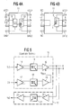
- FIG. 4A shows an example of a two-chip solution, whereby two chips 9, 10 (IC1, IC2) in a common Housing are housed and the first chip 9 for signal processing serves, while the second chip 10 the invention Tri-state driver arrangement 1 includes.
- FIG. 4A shows an embodiment with two separate chips 9, 10 requires two separate supply voltage connections VCC1, VCC2 and two separate ground connections GND1, GND2.
- the chip 9 there is also an input TxD for feeding Send data or for supplying a send signal and a release input EN provided.
- the chip 10, however, are also Outputs A, B shown in Figure 1 assigned.
- FIG. 4B shows an example of a one-chip solution, in this embodiment, only one supply voltage connection VCC2 and a ground connection GND2 required becomes. Those for supplying the input current to the tri-state driver arrangement 1 required connections are with + I or -I. Furthermore, there are the signal outputs A, B provided. The other connection pins are not occupied and labeled NC.
Landscapes
- Engineering & Computer Science (AREA)
- Power Engineering (AREA)
- Physics & Mathematics (AREA)
- Computer Hardware Design (AREA)
- Computing Systems (AREA)
- General Engineering & Computer Science (AREA)
- Mathematical Physics (AREA)
- Computer Networks & Wireless Communication (AREA)
- Signal Processing (AREA)
- Dc Digital Transmission (AREA)
- Transmitters (AREA)
Abstract
Description
Claims (17)
- Tri-State-Treiberanordnung,dadurch gekennzeichnet, dass der Koppler (2) ein Magnetkoppler ist.mit einem Koppler (2) zur potentialgetrennten Signalübertragung zwischen einem Eingang und einem Ausgang der Tri-State-Treiberanordnung (1),mit einem mit dem Ausgang gekoppelten Ausgangstreiber (8), undmit Steuermitteln (4 - 7) zur Ansteuerung des Ausgangstreibers (8), um diesen zum Senden von Daten in einen ersten oder zweiten Zustand und zum Deaktivieren der Tri-State-Treiberanordnung in einen dritten Zustand zu schalten,
- Tri-State-Treiberanordnung nach Anspruch 1,
dadurch gekennzeichnet, dass der Magnetkoppler (2) durch einen auf Grundlage des GMR ("Giant Magnet Resistor")-Effekts arbeitenden Sensor gebildet ist. - Tri-State-Treiberanordnung nach Anspruch 1 oder 2,
dadurch gekennzeichnet, dass die Steuermittel (4 - 7) derart ausgestaltet sind, dass sie eine von dem Magnetkoppler (2) gelieferte Ausgangsspannung (UOUT) auswerten, um davon abhängig den Ausgangstreiber (8) in den dritten Zustand zu schalten. - Tri-State-Treiberanordnung nach einem der vorhergehenden Ansprüche,
dadurch gekennzeichnet, dass der Magnetkoppler (2) derart ausgestaltet ist, dass er einen dem Eingang der Tri-State-Treiberanordnung (1) zugeführten Eingangsstrom (IIN) in eine entsprechende Ausgangsspannung (UOUT) umsetzt. - Tri-State-Treiberanordnung nach einem der vorhergehenden Ansprüche,
dadurch gekennzeichnet, dass die Steuermittel (4 - 7) derart ausgestaltet sind, dass sie den Ausgangstreiber (8) in den dritten Zustand schalten, falls eine von dem Magnetkoppler (2) gelieferte Ausgangsspannung (UOUT) in einem durch einen ersten Grenzwert (-UTH) und einen zweiten Grenzwert (+UTH) definierten Bereich liegt. - Tri-State-Treiberanordnung nach Anspruch 5,
dadurch gekennzeichnet, dass die Steuermittel einen Komparator (5) umfassen, welcher in Abhängigkeit von der Ausgangsspannung (UOUT) des Magnetkopplers (2) ein Steuersignal (UF) zur Ansteuerung des Ausgangstreibers (8) erzeugt, wobei das Steuersignal (UF) einen den Ausgangstreiber (8) aktivierenden ersten Wert annimmt, falls die Ausgangsspannung (UOUT) des Magnetkopplers (2) außerhalb des durch den ersten und zweiten Grenzwert (-UTH, +UTH) definierten Bereichs liegt, während das Steuersignal (UF) einen den Ausgangstreiber (8) deaktivierenden und in den dritten Zustand schaltenden zweiten Wert annimmt, falls die Ausgangsspannung (UOUT) des Magnetkopplers (2) innerhalb des durch den ersten und zweiten Grenzwert (-UTH, +UTH) definierten Bereichs liegt. - Tri-State-Treiberanordnung nach Anspruch 6,
dadurch gekennzeichnet, dass das von dem Komparator (5) erzeugte Steuersignal (UF) über einen Glättungsfilter (6) dem Ausgangstreiber (8) zugeführt ist. - Tri-State-Treiberanordnung nach einem der Ansprüche 5 - 7,
dadurch gekennzeichnet, dass die Steuermittel einen weiteren Komparator (4) umfassen, welche in Abhängigkeit von der Ausgangsspannung (UOUT) des Magnetkopplers (2) zum Senden von Daten eine Eingangsspannung (ULT) des Ausgangstreibers (8) auf einen ersten oder zweiten Wert setzt. - Tri-State-Treiberanordnung nach Anspruch 8,
dadurch gekennzeichnet, dass der weitere Komparator (4) die Eingangsspannung (ULT) des Ausgangstreibers (8) auf den ersten bzw. zweiten Wert setzt, falls die Ausgangsspannung (UOUT) des Magnetkopplers (2) größer als ein dritter Grenzwert (+UH) bzw. kleiner als ein vierter Grenzwert (-UH) ist. - Tri-State-Treiberanordnung nach Anspruch 9,
dadurch gekennzeichnet, dass der erste Grenzwert (-UTH) kleiner als der vierte Grenzwert (-UH) und der dritte Grenzwert (+UH) kleiner als der zweite Grenzwert (+UTH) ist. - Tri-State-Treiberanordnung nach einem der vorhergehenden Ansprüche,
dadurch gekennzeichnet, dass der Magnetkoppler (2) eine lineare Eingangsstrom/Ausgangsspannungskennlinie aufweist. - Tri-State-Treiberanordnung,dadurch gekennzeichnet, dass die Steuermittel (4 - 7) derart ausgestaltet sind, dass sie den Ausgangstreiber (8) in den dritten Zustand schalten, falls ein von dem Koppler (2) geliefertes Ausgangssignal (UOUT) in einem durch einen ersten Grenzwert (-UTH) und einen zweiten Grenzwert (+UTH) definierten Bereich liegt.mit einem Koppler (2) zur potentialgetrennten Signalübertragung zwischen einem Eingang und einem Ausgang der Tri-State-Treiberanordnung (1),mit einem mit dem Ausgang gekoppelten Ausgangstreiber (8), undmit Steuermitteln (4 - 7) zur Ansteuerung des Ausgangstreibers (8), um diesen zum Senden von Daten in einen ersten oder zweiten Zustand und zum Deaktivieren der Tri-State-Treiberanordnung in einen dritten Zustand zu schalten,
- Tri-State-Treiberanordnung nach Anspruch 12,
dadurch gekennzeichnet, dass die Steuermittel (4 - 7) derart ausgestaltet sind, dass sie den Ausgangstreiber (8) zum Senden von Daten in den ersten bzw. zweiten Zustand schalten, falls das von dem Koppler (2) gelieferte Ausgangssignal (UOUT) größer als ein dritter Grenzwert (+UH) bzw. kleiner als ein vierter Grenzwert (-UH) ist. - Tri-State-Treiberanordnung nach Anspruch 12 oder 13,
dadurch gekennzeichnet, dass der erste Grenzwert (-UTH) kleiner als der vierte Grenzwert (-UH) und der dritte Grenzwert (+UH) kleiner als der zweite Grenzwert (+UTH) ist. - Tri-State-Treiberanordnung nach einem der Ansprüche 12 - 14,
dadurch gekennzeichnet, dass die Tri-State-Treiberanordnung gemäß einem der Ansprüche 1 - 11 ausgestaltet ist. - Tri-State-Schnittstelle zur Anbindung eines Teilnehmers an eine Busleitung,
mit einer Tri-State-Treiberanordnung (1) nach einem der vorhergehenden Ansprüche, wobei die Tri-State-Treiberanordnung eingangsseitig über den Koppler (2) mit dem Teilnehmer und ausgangsseitig über den Ausgangstreiber (8) mit der Busleitung (A, B) zu verbinden ist. - Tri-State-Schnittstelle nach Anspruch 16,
dadurch gekennzeichnet, dass die Tri-State-Schnittstelle als RS-485-Schnittstelle ausgestaltet ist.
Applications Claiming Priority (2)
| Application Number | Priority Date | Filing Date | Title |
|---|---|---|---|
| DE10046806A DE10046806A1 (de) | 2000-09-21 | 2000-09-21 | Tri-State-Treiberanordnung |
| DE10046806 | 2000-09-21 |
Publications (3)
| Publication Number | Publication Date |
|---|---|
| EP1199857A2 true EP1199857A2 (de) | 2002-04-24 |
| EP1199857A3 EP1199857A3 (de) | 2006-06-21 |
| EP1199857B1 EP1199857B1 (de) | 2007-10-31 |
Family
ID=7657111
Family Applications (1)
| Application Number | Title | Priority Date | Filing Date |
|---|---|---|---|
| EP01121602A Expired - Lifetime EP1199857B1 (de) | 2000-09-21 | 2001-09-11 | Tri-State-Treiberanordnung |
Country Status (3)
| Country | Link |
|---|---|
| US (1) | US6670827B2 (de) |
| EP (1) | EP1199857B1 (de) |
| DE (2) | DE10046806A1 (de) |
Families Citing this family (7)
| Publication number | Priority date | Publication date | Assignee | Title |
|---|---|---|---|---|
| US6751110B2 (en) * | 2002-03-08 | 2004-06-15 | Micron Technology, Inc. | Static content addressable memory cell |
| DE10243197B4 (de) * | 2002-09-18 | 2011-05-05 | Infineon Technologies Ag | Digitales Signalübertragungsverfahren |
| DE10261216A1 (de) * | 2002-12-27 | 2004-07-22 | Infineon Technologies Ag | Kopplungsschaltung für eine Datenübertragung über ein Stromversorgungsnetz |
| US7259588B2 (en) * | 2003-07-29 | 2007-08-21 | Lexmark International Inc. | Tri-state detection circuit for use in devices associated with an imaging system |
| US7280294B2 (en) * | 2004-11-30 | 2007-10-09 | International Business Machines Corporation | Tri-state servowriter driver with slow return to zero |
| EP1947422B1 (de) * | 2007-01-19 | 2011-11-23 | SICK STEGMANN GmbH | Verfahren und Vorrichtung zur Parametrierung einer Messeinrichtung |
| JP6394275B2 (ja) * | 2014-10-22 | 2018-09-26 | ヤマハ株式会社 | 状態検出回路 |
Family Cites Families (6)
| Publication number | Priority date | Publication date | Assignee | Title |
|---|---|---|---|---|
| JP3054318B2 (ja) * | 1994-08-26 | 2000-06-19 | トヨタ自動車株式会社 | 双方向通信回路 |
| DE19718420A1 (de) * | 1997-04-30 | 1998-11-12 | Siemens Ag | Integrierte Datenübertragungsschaltung mit Potentialtrennung zwischen Ein- und Ausgangsschaltkreis |
| US6054780A (en) * | 1997-10-23 | 2000-04-25 | Analog Devices, Inc. | Magnetically coupled signal isolator using a Faraday shielded MR or GMR receiving element |
| FR2779250B1 (fr) * | 1998-06-02 | 2001-09-07 | Abb Control Sa | Circuit d'interface bistandard pour liaison serie |
| US6262600B1 (en) * | 2000-02-14 | 2001-07-17 | Analog Devices, Inc. | Isolator for transmitting logic signals across an isolation barrier |
| DE20021547U1 (de) * | 2000-12-20 | 2001-03-15 | Siemens AG, 80333 München | Bussystem mit dezentraler Peripherie |
-
2000
- 2000-09-21 DE DE10046806A patent/DE10046806A1/de not_active Ceased
-
2001
- 2001-09-11 DE DE50113189T patent/DE50113189D1/de not_active Expired - Lifetime
- 2001-09-11 EP EP01121602A patent/EP1199857B1/de not_active Expired - Lifetime
- 2001-09-20 US US09/957,632 patent/US6670827B2/en not_active Expired - Lifetime
Also Published As
| Publication number | Publication date |
|---|---|
| EP1199857A3 (de) | 2006-06-21 |
| DE50113189D1 (de) | 2007-12-13 |
| DE10046806A1 (de) | 2002-05-23 |
| EP1199857B1 (de) | 2007-10-31 |
| US6670827B2 (en) | 2003-12-30 |
| US20030025525A1 (en) | 2003-02-06 |
Similar Documents
| Publication | Publication Date | Title |
|---|---|---|
| DE19900869C2 (de) | Steuer- und Datenübertragungsanlage | |
| EP0830661B1 (de) | Anordnung zur galvanisch getrennten übertragung von hilfsenergie (gleichspannung) und informationen zu einer elektronischen einheit | |
| EP3766216B1 (de) | Sende-/empfangseinrichtung für ein bussystem und betriebsverfahren hierfür | |
| DE2953275C2 (de) | ||
| DE69317360T2 (de) | Sender/Empfänger Schaltung | |
| WO2019030080A1 (de) | Sende-/empfangseinrichtung für ein bussystem und verfahren zur reduzierung einer schwingneigung beim übergang zwischen unterschiedlichen bitzuständen | |
| DE19820248B4 (de) | Ausgangspufferschaltkreis mit umschaltbarem Ausgangs-Gleichtaktpegel | |
| EP1194858B1 (de) | Datenübertragungseinrichtung | |
| EP1199857B1 (de) | Tri-State-Treiberanordnung | |
| DE19803796B4 (de) | Ausgangspuffer zum Ansteuern einer symmetrischen Übertragungsleitung | |
| EP3665869B1 (de) | Sende-/empfangseinrichtung für ein bussystem und verfahren zur reduzierung einer schwingneigung beim übergang zwischen unterschiedlichen bitzuständen | |
| DE102020113663B4 (de) | Geräteeinheit, Mastereinheit und eine Verbindungsanordnung zur Punkt-zu-Punkt Kommunikation gemäß dem IO-Link Kommunikationsstandard | |
| DE3687047T2 (de) | Uebertragungsschaltung. | |
| EP1787206B1 (de) | Anordnung zur signalübertragung | |
| DE102020112985A1 (de) | IO-Link-Adapter | |
| DE9412303U1 (de) | Busteilnehmer | |
| EP0749070B1 (de) | Verfahren zum dezentralen Speisen eines Busses und Anordnung zum Durchführen des Verfahrens | |
| DE3429982A1 (de) | Schaltungsanordnung zum uebertragen von binaeren signalen | |
| DE69937034T2 (de) | Gesteuerte Stromquelle für Leitungstreiber beziehungsweise Leitungsempfänger | |
| EP1936895B1 (de) | Einrichtung zur Übertragung von Daten innerhalb eines leistungselektronischen Systems | |
| DE10130156B4 (de) | Verfahren und System zur bidirektionalen Signalübertragung | |
| DE10124176B4 (de) | Vorrichtung und Verfahren zum Reduzieren von Reflexionen in einem Speicherbussystem | |
| EP0235649A1 (de) | Schaltungsanordnung zur seriellen Datenübertragung zwischen mehreren Teilnehmerstellen | |
| DE102018220069A1 (de) | Reflexionsdämpfungsvorrichtung für einen Bus eines Bussystems und Verfahren zum Dämpfen von Reflexionen bei einer Datenübertragung in einem Bussystem | |
| DE2925747B1 (de) | Schaltungsanordnung fuer einen elektronischen Gleichstrom-Telegrafiesender |
Legal Events
| Date | Code | Title | Description |
|---|---|---|---|
| PUAI | Public reference made under article 153(3) epc to a published international application that has entered the european phase |
Free format text: ORIGINAL CODE: 0009012 |
|
| AK | Designated contracting states |
Kind code of ref document: A2 Designated state(s): AT BE CH CY DE DK ES FI FR GB GR IE IT LI LU MC NL PT SE TR |
|
| AX | Request for extension of the european patent |
Free format text: AL;LT;LV;MK;RO;SI |
|
| RIC1 | Information provided on ipc code assigned before grant |
Ipc: G06F 13/40 20060101ALI20060221BHEP Ipc: H03K 19/0175 20060101ALI20060221BHEP Ipc: H04L 25/02 20060101AFI20020215BHEP |
|
| PUAL | Search report despatched |
Free format text: ORIGINAL CODE: 0009013 |
|
| AK | Designated contracting states |
Kind code of ref document: A3 Designated state(s): AT BE CH CY DE DK ES FI FR GB GR IE IT LI LU MC NL PT SE TR |
|
| AX | Request for extension of the european patent |
Extension state: AL LT LV MK RO SI |
|
| 17P | Request for examination filed |
Effective date: 20060706 |
|
| 17Q | First examination report despatched |
Effective date: 20061025 |
|
| AKX | Designation fees paid |
Designated state(s): DE FR IT |
|
| GRAP | Despatch of communication of intention to grant a patent |
Free format text: ORIGINAL CODE: EPIDOSNIGR1 |
|
| GRAS | Grant fee paid |
Free format text: ORIGINAL CODE: EPIDOSNIGR3 |
|
| GRAA | (expected) grant |
Free format text: ORIGINAL CODE: 0009210 |
|
| AK | Designated contracting states |
Kind code of ref document: B1 Designated state(s): DE FR IT |
|
| REF | Corresponds to: |
Ref document number: 50113189 Country of ref document: DE Date of ref document: 20071213 Kind code of ref document: P |
|
| ET | Fr: translation filed | ||
| PLBE | No opposition filed within time limit |
Free format text: ORIGINAL CODE: 0009261 |
|
| STAA | Information on the status of an ep patent application or granted ep patent |
Free format text: STATUS: NO OPPOSITION FILED WITHIN TIME LIMIT |
|
| 26N | No opposition filed |
Effective date: 20080801 |
|
| REG | Reference to a national code |
Ref country code: FR Ref legal event code: PLFP Year of fee payment: 16 |
|
| REG | Reference to a national code |
Ref country code: FR Ref legal event code: PLFP Year of fee payment: 17 |
|
| REG | Reference to a national code |
Ref country code: FR Ref legal event code: PLFP Year of fee payment: 18 |
|
| PGFP | Annual fee paid to national office [announced via postgrant information from national office to epo] |
Ref country code: IT Payment date: 20190925 Year of fee payment: 19 |
|
| PGFP | Annual fee paid to national office [announced via postgrant information from national office to epo] |
Ref country code: DE Payment date: 20191121 Year of fee payment: 19 |
|
| PGFP | Annual fee paid to national office [announced via postgrant information from national office to epo] |
Ref country code: FR Payment date: 20200914 Year of fee payment: 20 |
|
| REG | Reference to a national code |
Ref country code: DE Ref legal event code: R119 Ref document number: 50113189 Country of ref document: DE |
|
| PG25 | Lapsed in a contracting state [announced via postgrant information from national office to epo] |
Ref country code: DE Free format text: LAPSE BECAUSE OF NON-PAYMENT OF DUE FEES Effective date: 20210401 |
|
| PG25 | Lapsed in a contracting state [announced via postgrant information from national office to epo] |
Ref country code: IT Free format text: LAPSE BECAUSE OF NON-PAYMENT OF DUE FEES Effective date: 20200911 |