EP1199751A2 - Chip-Anordnung - Google Patents
Chip-Anordnung Download PDFInfo
- Publication number
- EP1199751A2 EP1199751A2 EP01126917A EP01126917A EP1199751A2 EP 1199751 A2 EP1199751 A2 EP 1199751A2 EP 01126917 A EP01126917 A EP 01126917A EP 01126917 A EP01126917 A EP 01126917A EP 1199751 A2 EP1199751 A2 EP 1199751A2
- Authority
- EP
- European Patent Office
- Prior art keywords
- chip
- carrier
- substrate plate
- carrier chip
- component
- Prior art date
- Legal status (The legal status is an assumption and is not a legal conclusion. Google has not performed a legal analysis and makes no representation as to the accuracy of the status listed.)
- Withdrawn
Links
Images
Classifications
-
- H10W70/611—
-
- G—PHYSICS
- G01—MEASURING; TESTING
- G01N—INVESTIGATING OR ANALYSING MATERIALS BY DETERMINING THEIR CHEMICAL OR PHYSICAL PROPERTIES
- G01N21/00—Investigating or analysing materials by the use of optical means, i.e. using sub-millimetre waves, infrared, visible or ultraviolet light
- G01N21/01—Arrangements or apparatus for facilitating the optical investigation
-
- H10W90/00—
-
- H10W90/401—
-
- A—HUMAN NECESSITIES
- A61—MEDICAL OR VETERINARY SCIENCE; HYGIENE
- A61B—DIAGNOSIS; SURGERY; IDENTIFICATION
- A61B5/00—Measuring for diagnostic purposes; Identification of persons
- A61B5/145—Measuring characteristics of blood in vivo, e.g. gas concentration or pH-value ; Measuring characteristics of body fluids or tissues, e.g. interstitial fluid or cerebral tissue
- A61B5/14532—Measuring characteristics of blood in vivo, e.g. gas concentration or pH-value ; Measuring characteristics of body fluids or tissues, e.g. interstitial fluid or cerebral tissue for measuring glucose, e.g. by tissue impedance measurement
-
- A—HUMAN NECESSITIES
- A61—MEDICAL OR VETERINARY SCIENCE; HYGIENE
- A61B—DIAGNOSIS; SURGERY; IDENTIFICATION
- A61B5/00—Measuring for diagnostic purposes; Identification of persons
- A61B5/145—Measuring characteristics of blood in vivo, e.g. gas concentration or pH-value ; Measuring characteristics of body fluids or tissues, e.g. interstitial fluid or cerebral tissue
- A61B5/1468—Measuring characteristics of blood in vivo, e.g. gas concentration or pH-value ; Measuring characteristics of body fluids or tissues, e.g. interstitial fluid or cerebral tissue using chemical or electrochemical methods, e.g. by polarographic means
- A61B5/1473—Measuring characteristics of blood in vivo, e.g. gas concentration or pH-value ; Measuring characteristics of body fluids or tissues, e.g. interstitial fluid or cerebral tissue using chemical or electrochemical methods, e.g. by polarographic means invasive, e.g. introduced into the body by a catheter
-
- A—HUMAN NECESSITIES
- A61—MEDICAL OR VETERINARY SCIENCE; HYGIENE
- A61B—DIAGNOSIS; SURGERY; IDENTIFICATION
- A61B5/00—Measuring for diagnostic purposes; Identification of persons
- A61B5/44—Detecting, measuring or recording for evaluating the integumentary system, e.g. skin, hair or nails
- A61B5/441—Skin evaluation, e.g. for skin disorder diagnosis
-
- G—PHYSICS
- G01—MEASURING; TESTING
- G01N—INVESTIGATING OR ANALYSING MATERIALS BY DETERMINING THEIR CHEMICAL OR PHYSICAL PROPERTIES
- G01N33/00—Investigating or analysing materials by specific methods not covered by groups G01N1/00 - G01N31/00
- G01N33/48—Biological material, e.g. blood, urine; Haemocytometers
- G01N33/483—Physical analysis of biological material
- G01N33/487—Physical analysis of biological material of liquid biological material
- G01N33/48707—Physical analysis of biological material of liquid biological material by electrical means
Definitions
- the invention relates to a chip arrangement with a substrate plate, which has at least one breakthrough into which a Carrier chip is used or can be used on a carrier chip surface has at least one integrated conductor track, the at least one electrical or electronic component connects with at least one electrical connection contact, the carrier chip being inserted into the opening in this way or can be used that he ends with each other flat surface surfaces facing away from the substrate plate and thereby forms supernatants, on which the one surface protruding projection of the component and on which the other Surface protruding projection of the terminal contact arranged is, which is the component and the terminal contact interconnect interconnect the opening of the substrate plate interspersed, and being between the substrate plate and a seal is provided on the carrier chip.
- Such a chip arrangement is known from WO 87 05747 A, FIG. 4. It has a carrier chip with two ion-sensitive sensors on the conductor tracks with contacts of the carrier chip are connected.
- the carrier chip is in the opening one wall that he ends with each other protrudes opposite sides of the wall and thereby protrusions forms.
- the sensors are on one protrusion and on the other The connection contacts protruded.
- the conductor tracks, which connect the sensors to the connection contacts, are passed through the opening of the wall.
- Fig. 2 is also a non-generic Known chip arrangement that a substrate plate with a Breakthrough in which a carrier chip is inserted in such a way is that it has the ends facing away from each other on the flat side Exceeds surfaces of the substrate plate and thus protrusions forms.
- the carrier chip has an approximately U-shaped optical Waveguide on that with its two U-legs each penetrates the opening of the substrate plate, so that the free ends of the U-legs on one protrusion and the U-crossbar of the waveguide on the other projection are.
- the free end of one U-leg is an optical one Radiation emitter and that of the other U-leg with one facing the optical receiver.
- the latter is electric Conductor tracks of the carrier chip connected.
- the supernatant is an optical cell in the light guide switched, which consists of a chemosensitive material, that changes its optical properties and thus that in light guided by the waveguide modulates when it is a medium comes into contact with certain chemical properties. Also this chip arrangement does not permit scattered light or transmitted light measurement.
- the solution to this problem consists in an arrangement of the beginning mentioned type in that at least in the substrate plate two carrier chips are inserted that at least one of the carrier chips a component designed as a radiation emitter and the other carrier chip has at least one designed as a receiver, has the component associated with the radiation emitter and that a measurement section between the radiation emitter and the receiver is arranged.
- the two can Carrier chips optionally also a mechanical one Form filters so that only particles up to a certain by the distance between the carrier chips predetermined size in the Can reach measuring section.
- the electrical or electronic The component is on the one substrate plate surface located supernatant and thus over that in the carrier chip integrated conductor track connected to the contact at the other supernatant surface located.
- the connector is located on the electrical or electronic component facing away from the rear the substrate plate, so that in the area of the component having protruding conductor areas completely can be covered with a passivation layer.
- Such a passivation layer can be used, for example, in thin-film technology with great accuracy and moisture resistance are produced so that corrosion on the in the Carrier chip integrated track through the electrical or electronic component to be examined or treating medium is largely avoided.
- the between the carrier chip and the substrate plate arranged seal prevents that on the front of the substrate plate Medium to that arranged on the back of the substrate plate Connection contact can reach.
- the one in the substrate plate arranged breakthrough can for example by means of ultrasonic drilling be introduced into the substrate plate.
- the Chip arrangement is thus simple and inexpensive to manufacture. There is no need for a plastic compound to pour in bond pads can, the chip arrangement also has particularly compact dimensions on.
- the distance between the electrical or electronic component of a carrier chip and the another carrier chip to the diameter of a biological cell is adapted and preferably larger than 4 microns and smaller than Is 55 ⁇ m. This allows a cell between which the electrical or supernatant of the electronic component one carrier chip and the protrusion of the other carrier chip immediately attach to the component, while particles whose Dimensions are larger than the cell diameter of the device be kept away.
- At least one carrier chip is expediently detachable with the Connectable substrate plate.
- the carrier chip can then optionally can be easily replaced when the component is its has reached the intended lifespan or if it is by a Contact with a chemical to be examined or treated aggressive medium, should fail once.
- the invention is at least one carrier chip with a Breakthrough limiting wall area of the substrate plate glued.
- the one arranged between the carrier chip and the substrate plate Adhesive then serves on the one hand to attach the carrier chip to fix the substrate plate and on the other hand seals also the breakthrough of the substrate plate against the carrier chip, so that one at the front of the substrate plate in the area of medium located in the electrical or electronic component not to the rear of the Can get substrate plate.
- the glue is also the same Tolerances in the dimensions of the carrier chip and / or in the wall opening located in the substrate plate, in which the Carrier chip is inserted from. This is the chip arrangement even easier and cheaper to manufacture.
- the breakthrough limit Side surfaces of the substrate plate can then be rectangular be arranged to the flat side surface, what that Introduction of the opening in the substrate plate facilitated.
- a particularly advantageous embodiment of the invention provides before that the electrical or electronic component having Carrier chip surface of at least one carrier chip arranged obliquely to the flat surface of the substrate plate and preferably encloses an acute angle with it.
- the electrical or electronic component is then in a limited by the carrier chip and the substrate plate Corner area arranged so that only particles that a size not given by the dimensions of the corner area exceed with the electrical or electronic component can come into contact. This makes it easy built-up mechanical filter, the larger the penetration Particles to the device prevented.
- An advantageous embodiment of the invention provides that at least one carrier chip during assembly of the chip arrangement in at least two different layers in the breakthrough of the It can be used that at least in one of these layers an electrical or electronic component on one protruding a flat surface of the substrate plate Protrusion of the carrier chip and the chip (s) Component (s) assigned connector contact (s) to which the other protruding flat surface of the substrate plate Supernatant is arranged, and that in the other position of the carrier chip the component (s) and the connection contact (s) on the same, a flat surface of the substrate plate outstanding projection of the carrier chip arranged are.
- At least one carrier chip during assembly the chip arrangement in at least two different layers can be used in the opening of the substrate plate that the Carrier chip at least two electrical or electronic components has, each by means of at least one conductor track with at least one electrical assigned to them Connection contact are connected, and that depending on the selected Position of the carrier chip in each case at least one of these components on a surface projecting above a flat surface of the substrate plate Overhang of the carrier chip and the (these) this Connection contact (s) assigned to this component (s) on the protruding the other flat-side surface of the substrate plate Supernatant is arranged.
- the electrical or Electronic components can, for example, on the scope of Carrier chips integrated into its flat surface be, the carrier chip in different rotational positions with respect to the normal to this surface in the substrate plate can be used. Depending on the respective rotational position of the Carrier chips are then different components on the front arranged the substrate plate, while the associated Contacts are located on the back of each Substrate plate.
- the carrier chips abut each other so that the electrical or electronic component of a first carrier chip a second carrier chip is covered that as a spacer on the first carrier chip at least one laterally over the surface plane of the component protruding on the second carrier chip adjacent area and / or on the second carrier chip a laterally over the surface area covering the component projecting area adjacent to the first carrier chip is arranged such that between the component and the second carrier chip forms an access to the component Free space or gap is arranged.
- the area protruding from the component can with known methods of semiconductor technology, for example manufactured in mask technology with great dimensional accuracy be what in particular the realization of small gap dimensions or free spaces between the component and the second Carrier chip with closely toleranced dimensions enabled.
- the one second carrier chip adjacent to the above carrier chip region can have a substantially flat, facing the component, arranged parallel to its surface plane and preferably surface area adjacent to the above carrier chip area exhibit.
- the first carrier chip can be flat on the second carrier chip.
- the manufacture of the opposite Component protruding carrier chip area can for example in such a way that in the surface of the first carrier chip a recess is etched in which the component is arranged or that at certain points on the surface at least one layer of the first carrier chip is deposited or is applied.
- the substrate plate is made of an elastic Material exists.
- the substrate plate can then in the direction of extension be subjected to a tensile or compressive force. This allows the filter characteristics of the mechanical filter in a simple way to the size of the subject to be examined or treating particles are adjusted.
- the Substrate plate can also be designed as a bendable film. The Chip arrangement is then even easier to handle.
- the chip arrangement can be manufactured even more cost-effectively, if the substrate plate arranged at least four in one plane Has plate parts when adjacent to each other Plate parts each at their mutually facing edge areas preferably connected to each other by an adhesive and if the breakthrough is caused by one between the plate parts free space is formed.
- This can be a expensive drilling of the breakthrough, for example using ultrasound or a laser beam.
- the individual plate parts preferably each have straight edges and can be cut off, for example or saws can be cut.
- first plate parts each have at least one straight edge area, with which they are arranged parallel to each other and facing each other and if between the first plate parts in Direction of extension of the straight edge areas through the opening spaced from each other at least two second plate parts are arranged, each at their parallel to each other running edges with the straight edge areas of the first Plate parts are connected in particular by an adhesive.
- the abutting first and second plate parts can then before applying the glue towards their straight Border areas are shifted against each other, whereby the Length of the opening in the substrate plate changed easily and to the dimensions of the inserted Carrier chips can be customized.
- connection contacts On the back of the substrate plate facing the connection contacts can be arranged a circuit board with the Connection contacts connected or connectable connection points having.
- the circuit board can, for example, be an evaluation device and / or a control device and / or a power supply for the chip arrangement. This is on the back the substrate plate before touching one to be examined Medium protected.
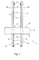
- a chip arrangement designated as a whole by 1, has a substrate plate 2, the breakthroughs 3 for two assigned to each other Carrier chips 4 has.
- the substrate plate 2 can for example consist of glass or a semiconductor material.
- One of the carrier chips 4 has an optical component 5 Transmitter and the other carrier chip 4 an optical receiver on. There is one between the optical transmitter and the receiver Measuring section formed.
- the chip arrangement can for example Transmitted light or scattered light measurement and / or as a light barrier be used.
- the components 5 are on a flat surface 6 of the Carrier chips 4 using methods of semiconductor technology in the carrier chip 4 integrated.
- the individual components 5 are each with one on the surface 6 of the carrier chip 4 or essentially parallel conductor track 7 with a Connection contact 8 connected to which an evaluation and control device can be connected.
- the carrier chips 4 are in the openings 3 of the substrate plate 2 used that the carrier chips 4 each with their Ends of the flat surfaces 9, 9 'facing away from one another protrude from the substrate plate 2 and thereby protrusions 10, 10 ' form that on the flat surfaces 9, 9 'of the substrate plate 2 project.
- the components 5 are on the a protrusion 10 and the electrical associated therewith Connection contacts 8 arranged on the other projection 10 '.
- the conductor tracks 7 each penetrate an opening 3 the substrate plate 2.
- the carrier chips 4 are each with the assigned to them Breakthrough 3 of the substrate plate 2 bounding edge the substrate plate 2 glued, the between this edge and the carrier chip 4 adhesive against the carrier chip 4 seals the substrate plate 2. So they are on the back the substrate plate 2 located contacts 8 well against a on the front of the components 5 facing the Substrate plate to be examined with the components 5 Medium that contains, for example, a nutrient medium biological cells can be shielded. A Corrosion on the connection contacts 8 due to in the nutrient medium contained components, such as salts or ions, is reliably avoided. Since the conductor tracks 7 the Breakthrough 3 of the substrate plate 2, in need of Production of the chip arrangement for connecting the components 5 no through-plating with the electrical connection contacts 8 be introduced into the substrate plate 2. The chip arrangement 1 is easy and inexpensive to manufacture.
- the carrier chips 4 can each be in the form of a rectangular plate be trained, with its chip level and its transverse to it running narrow side surfaces each perpendicular to the flat surfaces 9, 9 'of the substrate plate 2 are arranged is.
- the surfaces of the substrate plate delimiting the openings 3 2 are each perpendicular to their flat side Surfaces 9, 9 'arranged.
- the breakthroughs 3 easier in the manufacture of the chip arrangement in the substrate plate 2 are introduced.
- the conductor tracks 7 have an electrically insulating thin-film passivation layer 11 covered, for example Silicon oxide can exist. Through the passivation layer 11 the conductor tracks 7 are electrically well insulated from the nutrient medium. In addition, through the passivation layer 11 Corrosion on the conductor tracks 7 from contained in the nutrient medium Prevents salts or ions.
- the carrier chip 4 is also a component 5 can have, which emits an electric field, with which affects a cell located on the substrate plate 2 or can be stimulated.
Landscapes
- General Health & Medical Sciences (AREA)
- General Physics & Mathematics (AREA)
- Life Sciences & Earth Sciences (AREA)
- Chemical & Material Sciences (AREA)
- Analytical Chemistry (AREA)
- Biochemistry (AREA)
- Health & Medical Sciences (AREA)
- Immunology (AREA)
- Physics & Mathematics (AREA)
- Pathology (AREA)
- Measurement Of The Respiration, Hearing Ability, Form, And Blood Characteristics Of Living Organisms (AREA)
- Apparatus Associated With Microorganisms And Enzymes (AREA)
- Details Of Resistors (AREA)
- Structures For Mounting Electric Components On Printed Circuit Boards (AREA)
- Testing Of Individual Semiconductor Devices (AREA)
Abstract
Description
Claims (10)
- Chip-Anordnung (1) mit einer Substratplatte (2), die wenigstens einen Durchbruch (3) aufweist, in den ein Trägerchip (4) eingesetzt oder einsetzbar ist, der an einer Trägerchip-Oberfläche wenigstens eine integrierte Leiterbahn (7) aufweist, die wenigstens ein elektrisches oder elektronisches Bauelement (5) mit zumindest einem elektrischen Anschlußkontakt (8) verbindet, wobei der Trägerchip (4) derart in den Durchbruch (3) eingesetzt oder einsetzbar ist, daß er mit seinen Enden die einander abgewandten flachseitigen Oberflächen (9, 9') der Substratplatte (2) überragt und dadurch Überstände (10, 10') bildet, wobei an dem die eine Oberfläche (9) überragenden Überstand (10) das Bauelement und an dem die andere Oberfläche (9') überragenden Überstand (10') der Anschlußkontakt (8) angeordnet ist, wobei die das Bauelement (5) und den Anschlußkontakt (8) miteinander verbindende Leiterbahn (7) den Durchbruch (3) der Substratplatte (2) durchsetzt, und wobei zwischen der Substratplatte (2) und dem Trägerchip (4) eine Abdichtung vorgesehen ist, dadurch gekennzeichnet, daß in die Substratplatte (2) wenigstens zwei Trägerchips (4) eingesetzt sind, daß einer der Trägerchips (4) zumindest ein als Strahlungs-Emitter ausgebildetes Bauelement (5) und der andere Trägerchip (4) zumindest ein als Empfänger ausgebildetes, dem Strahlungs-Emitter zugeordnetes Bauelement (5) hat, und daß zwischen dem Strahlungs-Emitter und dem Empfänger eine Meßstrecke angeordnet ist.
- Chip-Anordnung (1) nach Anspruch 1, dadurch gekennzeichnet, daß der Abstand zwischen dem elektrischen oder elektronischen Bauelement (5) des einen Trägerchips (4) und dem anderen Trägerchip (4) an den Durchmesser einer biologischen Zelle angepaßt ist und vorzugsweise größer als 4 µm und kleiner als 55 µm ist.
- Chip-Anordnung (1) nach Anspruch 1 oder 2, dadurch gekennzeichnet, daß die das elektrische oder elektronische Bauelement (5) aufweisende Trägerchip-Oberfläche (6) des einen Trägerchips (4) und die dieser zugewandte Oberfläche (6) des anderen Trägerchips (4) trichterförmig schräg zueinander verlaufen.
- Chip-Anordnung (1) nach einem der Ansprüche 1 bis 3, dadurch gekennzeichnet, daß die Leiterbahn(en) (7) zumindest im Bereich eines ein elektrisches oder elektronisches Bauelement (5) aufweisenden Überstandes (10) mit einer elektrisch isolierenden Dünnfilm-Passivierungsschicht abgedeckt ist (sind).
- Chip-Anordnung (1) nach einem der Ansprüche 1 bis 4, dadurch gekennzeichnet, daß sich der Querschnitt der die elektrischen und/oder elektronischen Bauelemente (5) aufweisenden Überstände (10) jeweils ausgehend von der Oberfläche (9) der Substratplatte (2) zu der am weitesten vorstehenden Stelle des betreffenden Überstandes (10) verjüngt.
- Chip-Anordnung (1) nach einem der Ansprüche 1 bis 5, dadurch gekennzeichnet, daß wenigstens ein Trägerchip (4) bei der Montage der Chip-Anordnung (1) in wenigstens zwei unterschiedlichen Lagen in den Durchbruch (3) der Substratplatte (2) einsetzbar ist, daß in einer dieser Lagen wenigstens ein elektrisches oder elektronisches Bauelement (5) an einem eine flachseitige Oberfläche der Substratplatte (9) überragenden Überstand (10) des Trägerchips (4) und der (die) diesem (diesen) Bauelement(en) (5) zugeordnete(n) Anschlußkontakt(e) (8) an dem die andere flachseitige Oberfläche (9') der Substratplatte überragenden Überstand (10') angeordnet ist, und daß in der anderen Lage des Trägerchips (4) das (die) Bauelement(e) (5) und der (die) Anschlußkontakt(e) (8) an demselben, eine flachseitige Oberfläche der Substratplatte (9, 9') überragenden Überstand (10, 10') des Trägerchips (4) angeordnet sind.
- Chip-Anordnung (1) nach einem der Ansprüche 1 bis 6, dadurch gekennzeichnet, daß wenigstens ein Trägerchip (4) bei der Montage der Chip-Anordnung (1) in wenigstens zwei unterschiedlichen Lagen in den Durchbruch (3) der Substratplatte (2) einsetzbar ist, daß der Trägerchip (4) wenigstens zwei elektrische oder elektronische Bauelemente (5) aufweist, die jeweils mittels wenigstens einer Leiterbahn (7) mit zumindest einem ihnen jeweils zugeordneten elektrischen Anschlußkontakt (8) verbunden sind, und daß je nach gewählter Lage des Trägerchips (4) jeweils wenigstens eines dieser Bauelemente (5) an einem eine flachseitige Oberfläche der Substratplatte (9) überragenden Überstand (10) des Trägerchips (4) und der (die) diesem (diesen) Bauelement(en) (5) zugeordnete(n) Anschlußkontakt(e) (8) an dem die andere flachseitige Oberfläche (9') der Substratplatte überragenden Überstand (10') angeordnet ist.
- Chip-Anordnung (1) nach einem der Ansprüche 1 bis 7, dadurch gekennzeichnet, daß die Trägerchips (4) derart aneinander anliegen, daß das elektrische oder elektronische Bauelement (5) eines ersten Trägerchips (4) durch einen zweiten Trägerchip (4) überdeckt ist, daß als Abstandshalter an dem ersten Trägerchip (4) mindestens ein seitlich über die Oberflächenebene des Bauelements (5) vorstehender, an dem zweiten Trägerchip (4) anliegender Bereich und/oder an dem zweiten Trägerchip (4) ein seitlich über den das Bauelement (5) überdeckenden Oberflächenbereich vorstehender, an dem ersten Trägerchip (4) anliegender Bereich angeordnet ist, derart, daß zwischen dem Bauelement (5) und dem zweiten Trägerchip (4) ein einen Zugang zu dem Bauelement bildender Freiraum oder Spalt angeordnet ist.
- Chip-Anordnung (1) nach einem der Ansprüche 1 bis 8, dadurch gekennzeichnet, daß die Substratplatte (2) wenigstens vier in einer Ebene angeordnete Plattenteile aufweist, daß zueinander benachbarte Plattenteile jeweils an ihren einander zugewandten Randbereichen vorzugsweise durch eine Klebung miteinander verbunden sind, und daß der Durchbruch durch einen zwischen den Plattenteilen befindlichen Freiraum gebildet ist.
- Chip-Anordnung (1) nach einem der Ansprüche 1 bis 9, dadurch gekennzeichnet, daß wenigstens ein elektrisches oder elektronisches Bauelement (5) mit einer in den Trägerchip (4) integrierten Auswerte- und oder Steuereinheit verbunden ist.
Applications Claiming Priority (3)
| Application Number | Priority Date | Filing Date | Title |
|---|---|---|---|
| DE19829121 | 1998-06-30 | ||
| DE19829121A DE19829121C2 (de) | 1998-06-30 | 1998-06-30 | Anordnung mit einer Substratplatte und einem Chip |
| EP99112071A EP0969510B1 (de) | 1998-06-30 | 1999-06-23 | Chip-Anordnung |
Related Parent Applications (1)
| Application Number | Title | Priority Date | Filing Date |
|---|---|---|---|
| EP99112071A Division EP0969510B1 (de) | 1998-06-30 | 1999-06-23 | Chip-Anordnung |
Publications (2)
| Publication Number | Publication Date |
|---|---|
| EP1199751A2 true EP1199751A2 (de) | 2002-04-24 |
| EP1199751A3 EP1199751A3 (de) | 2005-12-07 |
Family
ID=26047125
Family Applications (2)
| Application Number | Title | Priority Date | Filing Date |
|---|---|---|---|
| EP01126917A Withdrawn EP1199751A3 (de) | 1998-06-30 | 1999-06-23 | Chip-Anordnung |
| EP01126916A Expired - Lifetime EP1189281B1 (de) | 1998-06-30 | 1999-06-23 | Chip-Anordnung |
Family Applications After (1)
| Application Number | Title | Priority Date | Filing Date |
|---|---|---|---|
| EP01126916A Expired - Lifetime EP1189281B1 (de) | 1998-06-30 | 1999-06-23 | Chip-Anordnung |
Country Status (1)
| Country | Link |
|---|---|
| EP (2) | EP1199751A3 (de) |
Families Citing this family (2)
| Publication number | Priority date | Publication date | Assignee | Title |
|---|---|---|---|---|
| US6228819B1 (en) | 1994-04-14 | 2001-05-08 | Rohm And Haas Company | Process for making a viscosity index improving copolymer |
| DE102014108356A1 (de) | 2014-06-13 | 2015-12-17 | Innovative Sensor Technology Ist Ag | Planares Heizelement mit einer PTC-Widerstandsstruktur |
Family Cites Families (10)
| Publication number | Priority date | Publication date | Assignee | Title |
|---|---|---|---|---|
| DE2736200A1 (de) * | 1977-08-11 | 1979-02-22 | Bbc Brown Boveri & Cie | Chemisch sensitiver feldeffekt- transistor und verfahren zur herstellung desselben |
| CA1250020A (en) * | 1985-01-23 | 1989-02-14 | Imants R. Lauks | Ambient sensing devices with isolation |
| WO1987005747A1 (en) * | 1986-03-21 | 1987-09-24 | Integrated Ionics, Inc. | Ambient sensing transcucer devices with isolation |
| DK409188D0 (da) * | 1988-07-21 | 1988-07-21 | Radiometer As | Fremgangsmaade til maaling af en karakteristik i et fluidum |
| US5046496A (en) * | 1989-04-26 | 1991-09-10 | Ppg Industries, Inc. | Sensor assembly for measuring analytes in fluids |
| DE4033741C2 (de) * | 1989-11-02 | 1994-03-31 | Falko Volkhardt E Dipl Tittel | Vorrichtung zum Nachweis von HIV-Antikörpern im Vollblut mit Anzeige des Ergebnisses |
| DE4013593A1 (de) * | 1990-04-27 | 1991-10-31 | Biotechnolog Forschung Gmbh | Verfahren und sensor fuer amperometrische messprinzipien mit dickschicht-biosensoren |
| SE511634C2 (sv) * | 1996-05-07 | 1999-11-01 | Samba Sensors Ab | Anordning för elektrooptisk mätning av tryck |
| DE19621227C2 (de) * | 1996-05-25 | 2003-02-20 | Micronas Gmbh | Sensorelement zum Nachweis von flüssigen, gasförmigen oder fluiden Substanzen |
| CA2259437C (en) * | 1996-07-03 | 2006-12-05 | Altea Technologies, Inc. | Multiple mechanical microporation of skin or mucosa |
-
1999
- 1999-06-23 EP EP01126917A patent/EP1199751A3/de not_active Withdrawn
- 1999-06-23 EP EP01126916A patent/EP1189281B1/de not_active Expired - Lifetime
Also Published As
| Publication number | Publication date |
|---|---|
| EP1189281A2 (de) | 2002-03-20 |
| EP1189281B1 (de) | 2007-08-22 |
| EP1199751A3 (de) | 2005-12-07 |
| EP1189281A3 (de) | 2005-12-07 |
Similar Documents
| Publication | Publication Date | Title |
|---|---|---|
| DE3118298C2 (de) | ||
| DE19907164C2 (de) | Meßeinrichtung sowie Verfahren zu deren Herstellung | |
| DE19852967A1 (de) | Meßeinrichtung sowie Verfahren zu deren Herstellung | |
| EP1367879A2 (de) | Elektrische Vorrichtung | |
| EP1236037B1 (de) | Sensor in einem gehäuse | |
| DE3044983A1 (de) | Integrierte schaltungsanordnung mit transistorelementen | |
| DE602005005646T2 (de) | Piezoelektrischer Resonator und Anordnung mit dem in ein Gehäuse eingeschlossenen Resonator | |
| EP1199751A2 (de) | Chip-Anordnung | |
| DE19861113C2 (de) | Anordnung mit einer Substratplatte und einem Chip | |
| DE102004010635A1 (de) | Vorrichtung zur Durchführung von Messungen an Biokomponenten | |
| DE102010027149A1 (de) | Verbiegbare Metallkernleiterplatte | |
| WO2014135560A1 (de) | Optoelektronisches bauelement und elektronisches gerät mit optoelektronischem bauelement | |
| DE19829121C2 (de) | Anordnung mit einer Substratplatte und einem Chip | |
| DE102005006280A1 (de) | Halbleiterbauteil mit einem Druckkontakt durch eine Gehäusemasse und Verfahren zur Herstellung desselben | |
| DE3001820A1 (de) | Magnetschranke | |
| EP0937315B1 (de) | Fluid mit mehreren, eine elektrisch leitfähige oberfläche aufweisenden partikeln | |
| EP0538432B1 (de) | Vorrichtung zum herstellen einer elektrischen schaltung, insbesondere für eine messonde und messonde | |
| WO2001088982A2 (de) | Gehäuseeinrichtung und darin zu verwendendes kontaktelement | |
| EP1573309A1 (de) | Halbleitersensor mit frontseitiger kontaktierung | |
| DE19741945C2 (de) | Magnetsensor | |
| DE3440180C2 (de) | ||
| DE102022200357A1 (de) | Verbindungselement zur elektrischen Kontaktierung von Schaltungsträgern | |
| DE3523440A1 (de) | Anzeigeeinrichtung mit einer elektrooptischen zelle | |
| DE29780368U1 (de) | Probenehmer für Flüssigkeiten | |
| DE102024207783A1 (de) | Abschirmgehäuse und Verfahren zum Ausbilden eines Abschirmgehäuses |
Legal Events
| Date | Code | Title | Description |
|---|---|---|---|
| PUAI | Public reference made under article 153(3) epc to a published international application that has entered the european phase |
Free format text: ORIGINAL CODE: 0009012 |
|
| AC | Divisional application: reference to earlier application |
Ref document number: 969510 Country of ref document: EP |
|
| AK | Designated contracting states |
Kind code of ref document: A2 Designated state(s): AT BE CH CY DE DK ES FI FR GB GR IE IT LI LU MC NL PT SE |
|
| PUAL | Search report despatched |
Free format text: ORIGINAL CODE: 0009013 |
|
| AK | Designated contracting states |
Kind code of ref document: A3 Designated state(s): AT BE CH CY DE DK ES FI FR GB GR IE IT LI LU MC NL PT SE |
|
| 17P | Request for examination filed |
Effective date: 20060117 |
|
| AKX | Designation fees paid |
Designated state(s): CH DE FR GB IT LI NL |
|
| 17Q | First examination report despatched |
Effective date: 20120109 |
|
| STAA | Information on the status of an ep patent application or granted ep patent |
Free format text: STATUS: THE APPLICATION IS DEEMED TO BE WITHDRAWN |
|
| 18D | Application deemed to be withdrawn |
Effective date: 20120103 |