EP1198043A2 - Method of fabricating a III-V compound semiconductor device with an Aluminium-compound layer - Google Patents
Method of fabricating a III-V compound semiconductor device with an Aluminium-compound layer Download PDFInfo
- Publication number
- EP1198043A2 EP1198043A2 EP01123215A EP01123215A EP1198043A2 EP 1198043 A2 EP1198043 A2 EP 1198043A2 EP 01123215 A EP01123215 A EP 01123215A EP 01123215 A EP01123215 A EP 01123215A EP 1198043 A2 EP1198043 A2 EP 1198043A2
- Authority
- EP
- European Patent Office
- Prior art keywords
- compound semiconductor
- layer
- semiconductor layer
- based compound
- forming
- Prior art date
- Legal status (The legal status is an assumption and is not a legal conclusion. Google has not performed a legal analysis and makes no representation as to the accuracy of the status listed.)
- Withdrawn
Links
Images

Classifications
-
- H—ELECTRICITY
- H01—ELECTRIC ELEMENTS
- H01L—SEMICONDUCTOR DEVICES NOT COVERED BY CLASS H10
- H01L21/00—Processes or apparatus adapted for the manufacture or treatment of semiconductor or solid state devices or of parts thereof
- H01L21/02—Manufacture or treatment of semiconductor devices or of parts thereof
- H01L21/04—Manufacture or treatment of semiconductor devices or of parts thereof the devices having at least one potential-jump barrier or surface barrier, e.g. PN junction, depletion layer or carrier concentration layer
- H01L21/18—Manufacture or treatment of semiconductor devices or of parts thereof the devices having at least one potential-jump barrier or surface barrier, e.g. PN junction, depletion layer or carrier concentration layer the devices having semiconductor bodies comprising elements of Group IV of the Periodic System or AIIIBV compounds with or without impurities, e.g. doping materials
- H01L21/30—Treatment of semiconductor bodies using processes or apparatus not provided for in groups H01L21/20 - H01L21/26
- H01L21/302—Treatment of semiconductor bodies using processes or apparatus not provided for in groups H01L21/20 - H01L21/26 to change their surface-physical characteristics or shape, e.g. etching, polishing, cutting
- H01L21/306—Chemical or electrical treatment, e.g. electrolytic etching
- H01L21/3065—Plasma etching; Reactive-ion etching
-
- H—ELECTRICITY
- H01—ELECTRIC ELEMENTS
- H01L—SEMICONDUCTOR DEVICES NOT COVERED BY CLASS H10
- H01L21/00—Processes or apparatus adapted for the manufacture or treatment of semiconductor or solid state devices or of parts thereof
- H01L21/02—Manufacture or treatment of semiconductor devices or of parts thereof
- H01L21/02104—Forming layers
- H01L21/02365—Forming inorganic semiconducting materials on a substrate
- H01L21/02367—Substrates
- H01L21/0237—Materials
- H01L21/02387—Group 13/15 materials
- H01L21/02392—Phosphides
-
- H—ELECTRICITY
- H01—ELECTRIC ELEMENTS
- H01L—SEMICONDUCTOR DEVICES NOT COVERED BY CLASS H10
- H01L21/00—Processes or apparatus adapted for the manufacture or treatment of semiconductor or solid state devices or of parts thereof
- H01L21/02—Manufacture or treatment of semiconductor devices or of parts thereof
- H01L21/02104—Forming layers
- H01L21/02365—Forming inorganic semiconducting materials on a substrate
- H01L21/02436—Intermediate layers between substrates and deposited layers
- H01L21/02439—Materials
- H01L21/02455—Group 13/15 materials
- H01L21/02461—Phosphides
-
- H—ELECTRICITY
- H01—ELECTRIC ELEMENTS
- H01L—SEMICONDUCTOR DEVICES NOT COVERED BY CLASS H10
- H01L21/00—Processes or apparatus adapted for the manufacture or treatment of semiconductor or solid state devices or of parts thereof
- H01L21/02—Manufacture or treatment of semiconductor devices or of parts thereof
- H01L21/02104—Forming layers
- H01L21/02365—Forming inorganic semiconducting materials on a substrate
- H01L21/02436—Intermediate layers between substrates and deposited layers
- H01L21/02439—Materials
- H01L21/02455—Group 13/15 materials
- H01L21/02463—Arsenides
-
- H—ELECTRICITY
- H01—ELECTRIC ELEMENTS
- H01L—SEMICONDUCTOR DEVICES NOT COVERED BY CLASS H10
- H01L21/00—Processes or apparatus adapted for the manufacture or treatment of semiconductor or solid state devices or of parts thereof
- H01L21/02—Manufacture or treatment of semiconductor devices or of parts thereof
- H01L21/02104—Forming layers
- H01L21/02365—Forming inorganic semiconducting materials on a substrate
- H01L21/02436—Intermediate layers between substrates and deposited layers
- H01L21/02494—Structure
- H01L21/02496—Layer structure
- H01L21/02505—Layer structure consisting of more than two layers
-
- H—ELECTRICITY
- H01—ELECTRIC ELEMENTS
- H01L—SEMICONDUCTOR DEVICES NOT COVERED BY CLASS H10
- H01L21/00—Processes or apparatus adapted for the manufacture or treatment of semiconductor or solid state devices or of parts thereof
- H01L21/02—Manufacture or treatment of semiconductor devices or of parts thereof
- H01L21/02104—Forming layers
- H01L21/02365—Forming inorganic semiconducting materials on a substrate
- H01L21/02518—Deposited layers
- H01L21/02521—Materials
- H01L21/02538—Group 13/15 materials
- H01L21/02543—Phosphides
-
- H—ELECTRICITY
- H01—ELECTRIC ELEMENTS
- H01L—SEMICONDUCTOR DEVICES NOT COVERED BY CLASS H10
- H01L21/00—Processes or apparatus adapted for the manufacture or treatment of semiconductor or solid state devices or of parts thereof
- H01L21/02—Manufacture or treatment of semiconductor devices or of parts thereof
- H01L21/02104—Forming layers
- H01L21/02365—Forming inorganic semiconducting materials on a substrate
- H01L21/02518—Deposited layers
- H01L21/02521—Materials
- H01L21/02538—Group 13/15 materials
- H01L21/02546—Arsenides
-
- H—ELECTRICITY
- H01—ELECTRIC ELEMENTS
- H01L—SEMICONDUCTOR DEVICES NOT COVERED BY CLASS H10
- H01L21/00—Processes or apparatus adapted for the manufacture or treatment of semiconductor or solid state devices or of parts thereof
- H01L21/02—Manufacture or treatment of semiconductor devices or of parts thereof
- H01L21/02104—Forming layers
- H01L21/02365—Forming inorganic semiconducting materials on a substrate
- H01L21/02612—Formation types
- H01L21/02617—Deposition types
- H01L21/0262—Reduction or decomposition of gaseous compounds, e.g. CVD
-
- H—ELECTRICITY
- H01—ELECTRIC ELEMENTS
- H01L—SEMICONDUCTOR DEVICES NOT COVERED BY CLASS H10
- H01L21/00—Processes or apparatus adapted for the manufacture or treatment of semiconductor or solid state devices or of parts thereof
- H01L21/02—Manufacture or treatment of semiconductor devices or of parts thereof
- H01L21/02104—Forming layers
- H01L21/02365—Forming inorganic semiconducting materials on a substrate
- H01L21/02612—Formation types
- H01L21/02617—Deposition types
- H01L21/02636—Selective deposition, e.g. simultaneous growth of mono- and non-monocrystalline semiconductor materials
- H01L21/02639—Preparation of substrate for selective deposition
-
- H—ELECTRICITY
- H01—ELECTRIC ELEMENTS
- H01L—SEMICONDUCTOR DEVICES NOT COVERED BY CLASS H10
- H01L21/00—Processes or apparatus adapted for the manufacture or treatment of semiconductor or solid state devices or of parts thereof
- H01L21/02—Manufacture or treatment of semiconductor devices or of parts thereof
- H01L21/02104—Forming layers
- H01L21/02365—Forming inorganic semiconducting materials on a substrate
- H01L21/02612—Formation types
- H01L21/02617—Deposition types
- H01L21/02636—Selective deposition, e.g. simultaneous growth of mono- and non-monocrystalline semiconductor materials
- H01L21/02647—Lateral overgrowth
-
- H—ELECTRICITY
- H01—ELECTRIC ELEMENTS
- H01L—SEMICONDUCTOR DEVICES NOT COVERED BY CLASS H10
- H01L33/00—Semiconductor devices with at least one potential-jump barrier or surface barrier specially adapted for light emission; Processes or apparatus specially adapted for the manufacture or treatment thereof or of parts thereof; Details thereof
- H01L33/005—Processes
- H01L33/0062—Processes for devices with an active region comprising only III-V compounds
-
- H—ELECTRICITY
- H01—ELECTRIC ELEMENTS
- H01S—DEVICES USING THE PROCESS OF LIGHT AMPLIFICATION BY STIMULATED EMISSION OF RADIATION [LASER] TO AMPLIFY OR GENERATE LIGHT; DEVICES USING STIMULATED EMISSION OF ELECTROMAGNETIC RADIATION IN WAVE RANGES OTHER THAN OPTICAL
- H01S5/00—Semiconductor lasers
- H01S5/20—Structure or shape of the semiconductor body to guide the optical wave ; Confining structures perpendicular to the optical axis, e.g. index or gain guiding, stripe geometry, broad area lasers, gain tailoring, transverse or lateral reflectors, special cladding structures, MQW barrier reflection layers
- H01S5/2054—Methods of obtaining the confinement
- H01S5/2081—Methods of obtaining the confinement using special etching techniques
-
- H—ELECTRICITY
- H01—ELECTRIC ELEMENTS
- H01S—DEVICES USING THE PROCESS OF LIGHT AMPLIFICATION BY STIMULATED EMISSION OF RADIATION [LASER] TO AMPLIFY OR GENERATE LIGHT; DEVICES USING STIMULATED EMISSION OF ELECTROMAGNETIC RADIATION IN WAVE RANGES OTHER THAN OPTICAL
- H01S5/00—Semiconductor lasers
- H01S5/20—Structure or shape of the semiconductor body to guide the optical wave ; Confining structures perpendicular to the optical axis, e.g. index or gain guiding, stripe geometry, broad area lasers, gain tailoring, transverse or lateral reflectors, special cladding structures, MQW barrier reflection layers
- H01S5/22—Structure or shape of the semiconductor body to guide the optical wave ; Confining structures perpendicular to the optical axis, e.g. index or gain guiding, stripe geometry, broad area lasers, gain tailoring, transverse or lateral reflectors, special cladding structures, MQW barrier reflection layers having a ridge or stripe structure
- H01S5/227—Buried mesa structure ; Striped active layer
- H01S5/2275—Buried mesa structure ; Striped active layer mesa created by etching
Abstract


Description
- The present invention relates to a method of fabricating a compound semiconductor device, which is suitable for reliably providing a compound semiconductor device, such as a semiconductor laser device, that has a device structure including an Al-based compound semiconductor layer and is manufactured by a fabrication process including a process of etching a semiconductor layer.
- Ordinary semiconductor laser devices are produced using a III-V compound semiconductor which consists of at least two types of elements selected from group III elements, such as A1, In and Ga, and group V elements, such as As and P. A semiconductor laser device has a ridge type device structure that is formed by selectively etching an epitaxial layer with a DH (Double Heterostructure) grown on, a semiconductor substrate, or has a buried type device structure that has an epitaxial layer for burying a mesa after the formation of the mesa. The latter type semiconductor laser device is advantageous in the better device characteristics, i.e., the stability or the like of the threshold current and the lateral mode.
- A conventional semiconductor laser device which has, for example, an AlGaInAs-based self-alignment structure (SAS) is manufactured as follows. First, as shown in Fig. 3A, an n-
InP buffer layer 2 is grown on an n-InP substrate 1 by using a metalorganic chemical vapor deposition (MOCVD). Next, anactive layer 3, which comprises a 100 nm-thick n-AlGaInAs (λg = 1000 nm) separate confinement hetereostructure (SCH) layer, an AlGaInAs/AlGaInAs multiquantum well (MQW) having a bandgap wavelength of, for example, 1300 nm and a well number of 6 and a 100 nm-thick p-AlGaInAs (λg = 1000 nm) SCH layer, is grown on thebuffer layer 2. Then, a 500 nm-thick n-AlInAscurrent blocking layer 4 and a 100 nm-thick p-InPupper cladding layer 5 are sequentially grown on theactive layer 3. - Next, an
SiN layer 6 and a resist film (not shown) are formed on the p-InPupper cladding layer 5, and a striped window having a width of 3 µm is formed in the resist film using photolithography. With the window-formed resist film used as a mask, theSiN layer 6 is etched with a hydrofluoric acid, after which the resist film is removed. Then, as shown in Fig. 3B, theupper cladding layer 5 and thecurrent blocking layer 4 are etched by using an etching apparatus. Then, as shown in Fig. 3C, theSiN layer 6 is removed and an p-InPupper cladding layer 7 is grown again on the entire epitaxial layer to the thickness of 2000 nm and a p-GaInAs contact layer 8 is grown on the p-InPupper cladding layer 7 by using the MOCVD. - Then, contact electrodes (not shown) are respectively formed on the top surface of the
contact layer 8 and the bottom surface of thesubstrate 1. Next, the semiconductor substrate on which a plurality of epitaxial layers including theactive layer 3 are formed is cleaved to desired sizes in a direction perpendicular to the stripe direction. This yields a semiconductor laser device of a 1300 nm-wavelength which has a self-alignment structure (SAS). - In fabricating a semiconductor laser device with such a device structure, however, the end face of the n-AlInAs
current blocking layer 4 is inevitably exposed through a groove formed by etching during the fabrication process. As a result, at the time the semiconductor substrate is returned to the MOCVD after etching, the exposed n-AlInAscurrent blocking layer 4 is exposed to the air or an oxygen atmosphere and is oxidized. This causes a crystal defect in the subsequent crystal growth. Such a crystal defect lowers the reliability of the semiconductor laser device. - Accordingly, it is an object of the present invention to provide a method of fabricating a compound semiconductor device, which can produce a semiconductor laser device without bringing about the aforementioned problem of oxidization of an Al-based compound semiconductor layer. The invention particularly aims at providing a method of reliably fabricating a compound semiconductor device, which has a device structure including an Al-based compound semiconductor layer and is produced by a fabrication process involving an etching process.
- A method of fabricating a compound semiconductor device according to the invention comprises a first step of sequentially performing vapor growth of a plurality of compound semiconductor layers including an Al-based compound semiconductor layer formed on a semiconductor substrate by using a vapor phase growth apparatus, thereby forming a semiconductor multilayer (epitaxial layer) having, for example, a double heterostructure (DH); a second step of selectively etching a specific compound semiconductor layer in the semiconductor multilayer in the vapor phase growth apparatus using a bromine-based gas, thereby forming a mesa; and a third step of growing a predetermined compound semiconductor layer on the semiconductor multilayer by using the vapor phase growth apparatus following the etching step.
- Other compound semiconductor layers besides the Al-based compound semiconductor layer in the semiconductor multilayer that is formed on the semiconductor substrate contain III-V compound semiconductors including at least two types selected from In, Ga, As and P. The selective etching of the semiconductor multilayer using a bromine-based gas is carried out using the Al-based compound semiconductor layer in the semiconductor multilayer as an etching stop layer.
- The invention is suitable for providing a semiconductor laser device having a buried ridge structure or a buried heterostructure on the semiconductor substrate by selective etching of the semiconductor multilayer and subsequent vapor phase growth of a compound semiconductor layer. It is preferable to use a MOCVD as the vapor phase growth apparatus. As vapor phase growth of a compound semiconductor layer on the semiconductor substrate, an etching process of the grown compound semiconductor layer using a bromine-based gas and subsequent vapor phase growth of a compound semiconductor layer are consecutively executed in a reactor of MOCVD, the compound semiconductor device is fabricated without exposing the Al-based compound semiconductor layer to air or an oxygen atmosphere.
- More specifically, in the vapor phase growth apparatus, a buffer layer of a compound semiconductor is formed on the semiconductor substrate, then an active layer including an Al-based compound semiconductor layer is formed on the buffer layer, then a cladding layer of a compound semiconductor other than an Al-based compound semiconductor is formed on the active layer. Then, the cladding layer on the active layer is selectively etched using the active layer as an etching stop layer, thereby forming a mesa, after which a compound semiconductor layer is formed to the thickness to bury the mesa.
- Alternatively, in the vapor phase growth apparatus, a buffer layer of a compound semiconductor is formed on the semiconductor substrate, then an etching stop layer of an Al-based compound semiconductor is formed on the buffer layer, then an active layer and a cladding layer both of a compound semiconductor other than an Al-based compound semiconductor are sequentially formed on the etching stop layer. Then, in the vapor phase growth apparatus, the active layer and the cladding layer on the etching stop layer are selectively etched, thereby forming a mesa, after which a compound semiconductor layer is formed to the thickness to bury the mesa.
-
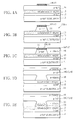
- Fig. 1A is a diagram showing a method of fabricating a compound semiconductor device according to a first embodiment of the invention and showing a first step in the fabrication of an SAS (Self-Alignment Structure) type semiconductor laser device;
- Fig. 1B is a diagram showing a second step following the step in Fig. 1A;
- Fig. 1C is a diagram showing a third step following the step in Fig. 1B;
- Fig. 1D is a diagram showing the schematic structure of the SAS type semiconductor laser device that is completed through a fourth step following the third step in Fig. 1C;
- Fig. 1E is a diagram showing another schematic structure of the SAS type semiconductor laser device that is manufactured by the fabrication method according to the invention;
- Fig. 2A is a diagram showing a method of fabricating a compound semiconductor device according to a second embodiment of the invention and showing a first step in the fabrication of a DH (Double Heterostructure) type semiconductor laser device;
- Fig. 2B is a diagram showing a second step following the step in Fig. 2A;
- Fig. 2C is a diagram showing a third step following the step in Fig. 2B;
- Fig. 2D is a diagram showing the schematic structure of the BH type semiconductor laser device that is completed through a fourth step following the third step in Fig. 2C;
- Fig. 3A is a diagram showing a first step in the fabrication of a conventional ordinary semiconductor laser device;
- Fig. 3B is a diagram showing a second step following the step in Fig. 3A; and
- Fig. 3C is a diagram showing the schematic structure of the semiconductor laser device that is completed through a third step following the second step in Fig. 3B.
-
- Referring to the accompanying drawings, a description of a method of fabricating a compound semiconductor device according to the invention will be given of the case of fabricating an AlGaInAs-based semiconductor laser device.
- Figs. 1A through 1D illustrate a fabrication process according to the first embodiment of the invention, step by step, in the case of fabricating a compound semiconductor laser device having a self-alignment structure (SAS).
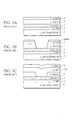
- First, using a metalorganic chemical vapor deposition (MOCVD), the fabrication of this semiconductor laser device is carried out by growing an n-
InP buffer layer 12 on an n-InP substrate 11, then growing anactive layer 13, which comprises a 100 nm-thick n-AlGaInAs (λg = 1000 nm) SCH layer, an AlGaInAs/AlGaInAs multiquantum well having, for example, a bandgap wavelength of 1300 nm and a well number of 6 and a 100 nm-thick p-AlGaInAs (λg = 1000 nm) SCH layer, on thebuffer layer 12, then growing a 300 nm-thick p-InPupper cladding layer 14 on theactive layer 13, as shown in Fig. 1A (first step). - Next, an
SiN layer 15 is formed on the p-InPupper cladding layer 14 and is patterned by photolithography so that theSiN layer 15 having a width of 3 µm is formed in the forward mesa direction. Then, with theSiN layer 15 used as a mask, the p-InPupper cladding layer 14 is etched in a reactor of the MOCVD with a bromine-based gas, specifically, carbon tetrabromide (CBr4), thereby forming a mesa as shown in Fig. 1B (second step). The etching process is performed, for example, at an etching temperature of 600°C and with the CBr4 fed at a rate of 3 µmol/min in the PH3 atmosphere. - In the fabrication of samples by the present inventors, the p-InP
upper cladding layer 14 was etched for approximately 15 minutes at an etching rate of 20 nm/min. The results showed that, as shown in Fig. 1B, a mesa without side etching and with an excellent dimension controllability with theSiN layer 15 as a mask could be formed. It was also confirmed that etching completely stopped in the depth direction on the top surface of the p-AlGaInAs (λg = 1000 nm) SCH layer and the p-AlGaInAs layer served as an etching stop layer with respect to etching of the p-InPupper cladding layer 14 by CBr4. - Following the etching process, buried growth of a compound semiconductor layer on the epitaxial layer is performed in the reactor of the MOCVD. In the buried growth, first, an n-AlInAs
current blocking layer 16 is grown to the thickness of, for example, 300 nm, then a 10 nm-thick p-InP layer 17 is grown on the n-AlInAscurrent blocking layer 16, as shown in Fig. 1C (third step). - The growth of the n-AlInAs
current blocking layer 16 was carried out at a growth temperature of 600°C and a growth rate of 30 nm/min. It was confirmed that at the time of growing the n-AlInAscurrent blocking layer 16, feeding CBr4 in the reactor of the MOCVD could suppress precipitation of a polycrystal on theSiN layer 15. - Then, the
SiN layer 15 is removed using buffered hydrofluoric acid, after which in the reactor of the MOCVD,. as shown in Fig. 1D, a p-InP upper cladding layer 18 is grown to the thickness of 2000 nm and a p-GaInAs contact layer 19 is grown on the cladding layer 18 to the thickness of 300 nm. Then, contact electrodes (not shown) are respectively formed on the top surface of thecontact layer 19 and the bottom surface of thesubstrate 11. Next, the semiconductor substrate on which the epitaxial layers having the above-described device structure are formed is cleaved to desired sizes in a direction perpendicular to the stripe direction. This yields a semiconductor laser device of a 1300 nm-wavelength range which has a buried ridge structure. - It was confirmed that the compound semiconductor laser device (compound semiconductor device) produced in the above-described manner, which basically had a device structure similar to that of the conventional semiconductor laser device shown in Fig. 3C, had its performances improved significantly in the threshold current and slope efficiency.
- In short, the first embodiment of the invention comprises growing a DH epitaxial layer on the n-
InP substrate 11 in the reactor of the MOCVD (first step), then selectively etching the epitaxial layer using CBr4, thereby forming a mesa (second step), then growing the epitaxial layer for burying the mesa in the reactor (third step), thus yielding an SAS semiconductor laser device. - As the fabrication process is entirely executed in the reactor of the MOCVD although the fabrication process includes an etching process, the Al-based compound semiconductor layer that comprises the p-AlGaInAs layer in the
active layer 13, which is a part of the device structure, and the n-AlInAscurrent blocking layer 16 is not exposed to the air or an oxygen atmosphere or the like. Accordingly, the Al-based compound semiconductor layer (the p-AlGaInAs layer and the n-AlInAs layer) is not oxidized, which would otherwise cause a crystal defect in the subsequent regrowth of the epitaxial layer. Further, as mentioned earlier, side etching hardly occurs at the time of etching the epitaxial layer (InP layer) using the bromine-based gas (CBr4). Furthermore, as the p-AlGaInAs layer serves as an etching stop layer, a semiconductor laser device whose device structure has a high dimension precision can be realized. In this respect too, the embodiment demonstrates its impressive effect of enhancing the operational reliability of the semiconductor laser device (compound semiconductor device). - A
GaInAsP layer 20 may be provided in the upper cladding layer that comprises the p-InP layer 14 in the above-described device structure as shown in Fig. 1E, so that the transverse mode of the semiconductor laser is controlled. In this case, in the first step in the above-described fabrication process, theGaInAsP layer 20 may be grown on theactive layer 13 after which the p-InPupper cladding layer 14 may be grown on theGaInAsP layer 20. It was confirmed that the provision of theGaInAsP layer 20 could ensure better laser characteristics. - The fabrication of a BH semiconductor laser device according to a second embodiment proceeds as follows. The second embodiment will be described with reference to Figs. 2A through 2D. The fabrication of this semiconductor laser device is carried out by using an MOCVD. First, as shown in Fig. 2A, an n-
InP buffer layer 22 is grown on an n-InP substrate 21, then an n-AlInAsetching stop layer 23 is formed 10 nm-thick on thebuffer layer 22. Next, an n-InP undercladding layer 24 having a thickness of 300 nm is grown on theetching stop layer 23, then a GaInAsP-based.active layer 25, which comprises a 100 nm-thick n-GaInAsP (λg = 1100 nm) SCH layer, a GaInAsP/GaInAsP multiquantum well having, for example, a bandgap wavelength of 1300 nm and a well number of 6 and a 100 nm-thick p-GaInAsP (λg = 1100 nm) SCH layer, is grown on the n-InP undercladding layer 24. Then, a 200 nm-thick p-InPupper cladding layer 26 is grown on the active layer 25 (first step). - Next, an
SiN layer 27 having a width of, for example, 2 µm, is formed on the p-InPupper cladding layer 26 in the backward mesa direction. With theSiN layer 27 used as a mask, the p-InPupper cladding layer 26, the GaInAsP-basedactive layer 25 and the n-InP undercladding layer 24 are sequentially etched in the reactor of the MOCVD using CBr4, thereby forming a mesa as shown in Fig. 2B (second step). The etching process is performed, for example, at an etching temperature of 600°C and with the CBr4 fed at a rate of 3 µmol/min in the PH3 atmosphere. - The etching rate in this case is 20 nm/min for the InP layers 26 and 24, and is 10 nm/min for the GaInAsP-based
active layer 25. In the second embodiment, etching was carried out for approximately 60 minutes. The results showed that, as shown in Fig. 2B, a mesa without side etching and with an excellent dimension controllability with the SiN resistfilm 27 as a mask could be formed. It was also confirmed that etching completely stopped in the depth direction on the top surface of the n-AlInAsetching stop layer 23 and the n-AlInAsetching stop layer 23 served as an etching stop layer with respect to the etching of the p-InP and GaInAsP-based semiconductor layers by CBr4. - Following the etching process, buried growth of a compound semiconductor layer on the epitaxial layer is performed in the reactor of the MOCVD. In the buried growth, first, a p-
InP layer 28 is grown to the thickness of, for example, 300 nm, then an n-InP layer 29 is grown 200 nm-thick on the p-InP layer 28, as shown in Fig. 2C (third step). - The growth of the InP layers 28 and 29 was performed at a growth temperature of 600°C and a growth rate of 60 nm/min.
- Then, the
SiN layer 27 is removed using buffered hydrofluoric acid, after which in the reactor of the MOCVD, as shown in Fig. 2D, a p-InPupper cladding layer 30 is grown to the thickness of 2000 nm and a p-GaInAs contact layer 31 is grown on theupper cladding layer 30 to the thickness of 300 nm. Then, contact electrodes (not shown) are respectively formed on the top surface of thecontact layer 19 and the bottom surface of thesubstrate 11. Next, the semiconductor substrate on which the epitaxial layers having the above-described device structure are formed is cleaved to desired sizes in a direction perpendicular to the stripe direction. This yields a semiconductor laser device of a 1300-nm wavelength range. - In the above-described fabrication of the semiconductor laser device of the second embodiment, as per the first embodiment, the epitaxial growth of a compound semiconductor layer on the
semiconductor substrate 21, the selective etching of the epitaxial layer and the subsequent regrowth of a compound semiconductor layer are all executed in the reactor of the MOCVD. Therefore, the GaInAsP-basedactive layer 25 whose oxidation should be avoided will not be exposed to the air or an oxygen atmosphere. It is thus possible to easily fabricate a semiconductor laser device (compound semiconductor device) that has a device structure of high dimension precision and an excellent crystalline characteristic and demonstrate a highly reliable operation. - The invention is not limited to those two embodiments. Although prevention of oxidation of the GaInAsP layer or the AlGaInAs layer that is grown on the InP substrate is discussed in the foregoing description of the embodiments, the invention can also be adapted to the case where an AlGaAs-based or AlGaInP-based compound semiconductor layer is grown on a GaAs substrate. That is, the invention can effectively be adapted to the case of fabricating a semiconductor device that is constructed to have a lamination of a III-V compound semiconductor which contains at least two kinds selected from In, Ga, As and P and an Al-based compound semiconductor.
- The invention is applicable not only to the fabrication of a semiconductor laser device that involves an etching process for forming a mesa and the subsequent epitaxial growth, but also to the fabrication of a compound semiconductor device that involves an etching process for forming a butt-joint and the subsequent epitaxial growth. Further, the above-described etching process is applicable to the case of using a bromine-based gas other than CBr4, such as CH3Br, as an etching gas. The invention may be modified in other forms without departing from the spirit or scope of the invention.
- According to the present invention, as described above, as etching of an epitaxial layer is carried out using a bromine-based gas in a vapor phase growth apparatus, it is possible to consecutively execute the growth of a compound semiconductor layer, the mentioned etching process, and the subsequent regrowth of a compound semiconductor layer. Even in the case of fabricating a compound semiconductor device whose structure includes an Al-based compound semiconductor layer whose oxidation should be avoided, therefore, oxidation-originated crystal defects and side etching will not occur. This makes it possible to control the dimension at a high accuracy and thus easily fabricate a highly reliable compound semiconductor device which has an excellent crystalline characteristic.
- As etching is performed while using the Al-based compound semiconductor layer as an etching stop layer to stop etching by a bromine-based gas, the invention also demonstrate an effect of sufficiently enhancing the etching control precision for epitaxial layers.
- Where technical features mentioned in any claim are followed by reference signs, those reference signs have been included for the sole purpose of increasing the intelligibility of the claims and accordingly, such reference signs do not have any limiting effect on the scope of each element identified by way of example by such reference signs.
Claims (17)
- A method of fabricating a compound semiconductor device, comprising steps of:selectively etching with a bromine-based gas in a vapor phase growth apparatus a specific compound semiconductor layer, said specific compound semiconductor layer being a layer of a semiconductor multilayer structure, said semiconductor multilayer structure including an Al-based compound semiconductor layer as part of a plurality of semiconductor layers formed on a semiconductor substrate; andgrowing in said vapor phase growth apparatus a predetermined compound semiconductor layer on said semiconductor multilayer structure, following said etching step.
- The method of Claim 1, wherein:except for said Al-based compound semiconductor layer, said plurality of semiconductor layers containing III-V compounds including at least two of In, Ga, As, and P.
- The method of Claim 1, wherein:said selective etching step includes limiting an etch depth with said Al-based compound semiconductor layer serving as an etch stop.
- The method of Claim 1, wherein:said growing step comprises growing the predetermined compound semiconductor layer so as to form at least one of a buried ridge structure and a buried heterostructure structure on said substrate as part of a semiconductor laser device.
- The method of Claim 1, wherein:said growing step includes growing said predetermined compound semiconductor layer by MOCVD.
- The method of Claim 1, wherein:said semiconductor substrate including at least one of an InP material and a GaAs material.
- A method of fabricating a compound semiconductor device, comprising steps of:sequentially growing via vapor growth in a vapor phase growth apparatus a plurality of compound semiconductor layers so as to form a semiconductor multilayer structure, said semiconductor multilayer structure includingan Al-based compound semiconductor layer, anda predetermined compound semiconductor layer;forming a mesa by selectively etching using a bromine-based gas in said vapor phase growth apparatus, except for said Al-based compound semiconductor layer, the predetermined compound semiconductor layer; andregrowing at least a portion of the predetermined compound semiconductor layer on said semiconductor multilayer in said vapor phase growth apparatus following said forming a mesa step.
- The method of Claim 7, wherein:said sequentially growing step includesforming a buffer layer of a compound semiconductor layer on said semiconductor substrate,forming an active layer including the Al-based compound semiconductor layer on said buffer layer, andforming a cladding layer of a compound semiconductor layer other than said Al-based compound semiconductor on said active layer; andsaid selectively etching step includes etching said cladding layer on said active layer using said active layer as an etch stop.
- The method of Claim 7, wherein:said sequentially performing step includes forming a buffer layer of a compound semiconductor material on said semiconductor substrate,forming an etch stop of an Al-based compound semiconductor material on said buffer layer,sequentially forming an active layer and a cladding layer both of a compound semiconductor material other than an Al-based compound semiconductor material used on said etch stop; andsaid selectively etching step includes selectively etching said active layer and said cladding layer on said etch stop.
- The method of Claim 7, wherein:said compound semiconductor device being a semiconductor laser.
- The method of Claim 7, wherein:said semiconductor substrate including at least one of an InP material and a GaAs material.
- A method of fabricating a compound semiconductor device, comprising steps for:selectively forming by etching a specific compound semiconductor layer, said specific compound semiconductor layer being a layer of a semiconductor multilayer structure, said semiconductor multilayer structure including an Al-based compound semiconductor layer as part of a plurality of semiconductor layers formed on a semiconductor substrate, said selectively forming step includes a substep forforming said Al-based compound semiconductor layer without exposing an abutting surface of said Al-based compound semiconductor layer to air or oxygen so as to prevent said abutting surface from becoming oxidized; andgrowing in said vapor phase growth apparatus a predetermined compound semiconductor layer on said semiconductor multilayer structure so as to abut and cover said abutting surface of said Al-based compound semiconductor layer.
- The method of Claim 12, wherein:except for said Al-based compound semiconductor layer, said plurality of semiconductor layers containing III-V compounds including at least two of In, Ga, As, and P.
- The method of Claim 12, wherein:said selectively forming by etching step includes limiting an etch depth with said Al-based compound semiconductor layer serving as an etch stop.
- The method of Claim 12, wherein:said growing step comprises growing the predetermined compound semiconductor layer so as to form at least one of a buried ridge structure and a buried heterostructure structure on said substrate as part of a semiconductor laser device.
- The method of Claim 12, wherein:said growing step includes growing said predetermined compound semiconductor layer by MOCVD.
- The method of Claim 12, wherein:said semiconductor substrate including at least one of an InP material and a GaAs material.
Applications Claiming Priority (2)
| Application Number | Priority Date | Filing Date | Title |
|---|---|---|---|
| JP2000307637 | 2000-10-06 | ||
| JP2000307637A JP2002118327A (en) | 2000-10-06 | 2000-10-06 | Method for manufacturing compound semiconductor device |
Publications (2)
| Publication Number | Publication Date |
|---|---|
| EP1198043A2 true EP1198043A2 (en) | 2002-04-17 |
| EP1198043A3 EP1198043A3 (en) | 2004-04-28 |
Family
ID=18788117
Family Applications (1)
| Application Number | Title | Priority Date | Filing Date |
|---|---|---|---|
| EP01123215A Withdrawn EP1198043A3 (en) | 2000-10-06 | 2001-10-01 | Method of fabricating a III-V compound semiconductor device with an Aluminium-compound layer |
Country Status (4)
| Country | Link |
|---|---|
| US (1) | US20020043209A1 (en) |
| EP (1) | EP1198043A3 (en) |
| JP (1) | JP2002118327A (en) |
| CA (1) | CA2358006A1 (en) |
Cited By (1)
| Publication number | Priority date | Publication date | Assignee | Title |
|---|---|---|---|---|
| GB2411520A (en) * | 2004-02-25 | 2005-08-31 | Agilent Technologies Inc | Method of forming laser mesa by reactive ion etching followed by in situ etching in regrowth reactor |
Families Citing this family (7)
| Publication number | Priority date | Publication date | Assignee | Title |
|---|---|---|---|---|
| CA2328641A1 (en) * | 2000-12-15 | 2002-06-15 | Nortel Networks Limited | Confinement layer of buried heterostructure semiconductor laser |
| JP2003133642A (en) * | 2001-10-19 | 2003-05-09 | Hitachi Ltd | Semiconductor laser device and photoelectron device |
| KR100630197B1 (en) * | 2004-11-03 | 2006-09-29 | 삼성전자주식회사 | Fabricating method of semicondouctor optical device for flip-chip bonding |
| JP2011507273A (en) * | 2007-12-10 | 2011-03-03 | スリーエム イノベイティブ プロパティズ カンパニー | Semiconductor light emitting device and manufacturing method thereof |
| JP2012169540A (en) * | 2011-02-16 | 2012-09-06 | Furukawa Electric Co Ltd:The | Semiconductor element manufacturing method and semiconductor element |
| CN108885979B (en) * | 2016-03-11 | 2024-04-09 | 应用材料公司 | Aluminum electroplating and oxide formation as barrier layers for aluminum semiconductor processing equipment |
| WO2023231353A1 (en) * | 2022-05-30 | 2023-12-07 | 青岛海信宽带多媒体技术有限公司 | Laser chip preparation method, laser chip, and optical module |
Citations (3)
| Publication number | Priority date | Publication date | Assignee | Title |
|---|---|---|---|---|
| EP0374036A2 (en) * | 1988-12-13 | 1990-06-20 | Fujitsu Limited | Method of fabricating a semiconductor device using U.V. assisted selective multilayer etching |
| EP0709902A1 (en) * | 1994-10-26 | 1996-05-01 | Mitsubishi Chemical Corporation | Semiconductor device and method for manufacturing the same |
| US5942447A (en) * | 1996-09-06 | 1999-08-24 | Mitsubishi Denki Kabushiki Kaisha | Method of selectively etching compound semiconductor and method of manufacturing compound semiconductor device using the selective etching method |
Family Cites Families (5)
| Publication number | Priority date | Publication date | Assignee | Title |
|---|---|---|---|---|
| JP2817286B2 (en) * | 1989-11-29 | 1998-10-30 | 富士通株式会社 | Method for manufacturing semiconductor device |
| JPH06232099A (en) * | 1992-09-10 | 1994-08-19 | Mitsubishi Electric Corp | Manufacture of semiconductor device, manufacturing device of semiconductor device, manufacture of semiconductor laser, manufacture of quantum wire structure, and crystal growth method |
| JPH07249581A (en) * | 1994-03-09 | 1995-09-26 | Fujitsu Ltd | Iii-v compound semiconductor crystal growth |
| JP3478005B2 (en) * | 1996-06-10 | 2003-12-10 | ソニー株式会社 | Method for etching nitride-based compound semiconductor and method for manufacturing semiconductor device |
| JPH1032176A (en) * | 1996-07-17 | 1998-02-03 | Hitachi Ltd | Etching method and manufacturing method of semiconductor device |
-
2000
- 2000-10-06 JP JP2000307637A patent/JP2002118327A/en active Pending
-
2001
- 2001-08-27 US US09/938,640 patent/US20020043209A1/en not_active Abandoned
- 2001-09-20 CA CA002358006A patent/CA2358006A1/en not_active Abandoned
- 2001-10-01 EP EP01123215A patent/EP1198043A3/en not_active Withdrawn
Patent Citations (3)
| Publication number | Priority date | Publication date | Assignee | Title |
|---|---|---|---|---|
| EP0374036A2 (en) * | 1988-12-13 | 1990-06-20 | Fujitsu Limited | Method of fabricating a semiconductor device using U.V. assisted selective multilayer etching |
| EP0709902A1 (en) * | 1994-10-26 | 1996-05-01 | Mitsubishi Chemical Corporation | Semiconductor device and method for manufacturing the same |
| US5942447A (en) * | 1996-09-06 | 1999-08-24 | Mitsubishi Denki Kabushiki Kaisha | Method of selectively etching compound semiconductor and method of manufacturing compound semiconductor device using the selective etching method |
Non-Patent Citations (4)
| Title |
|---|
| ARAKAWA S ET AL: "In-situ etching of semiconductor with CBr4 in MOCVD reactor" CONFERENCE PROCEEDINGS. 2001 INTERNATIONAL CONFERENCE ON INDIUM PHOSPHIDE AND RELATED MATERIALS. IPRM. NARA, JAPAN, MAY 14 - 18, 2001, INTERNATIONAL CONFERENCE ON INDIUM PHOSPHIDE AND RELATED MATERIALS, NEW YORK, NY: IEEE, US, vol. CONF. 13, 14 May 2001 (2001-05-14), pages 71-74, XP010546976 ISBN: 0-7803-6700-6 * |
| HOU H Q ET AL: "In situ etching of GaAs by AsCl3 for regrowth on AlGaAs in metalorganic vapor-phase epitaxy" JOURNAL OF CRYSTAL GROWTH, NORTH-HOLLAND PUBLISHING CO. AMSTERDAM, NL, vol. 195, no. 1-4, 15 December 1998 (1998-12-15), pages 199-204, XP004154260 ISSN: 0022-0248 * |
| IKAWA S ET AL: "AIGAAS-GAAS BURIED HETEROSTRUCTURE LASER WITH VERTICALLY ETCHED FACETS AND WIDE-BANDGAP OPTICAL WINDOWS BY IN SITU C2H5CI GAS-PHASEETCHING AND MOCVD REGROWTH" IEEE PHOTONICS TECHNOLOGY LETTERS, IEEE INC. NEW YORK, US, vol. 9, no. 6, 1 June 1997 (1997-06-01), pages 719-721, XP000692401 ISSN: 1041-1135 * |
| INOUE Y ET AL: "FABRICATION OF ALXGA1-XAS BURIED HETEROSTRUCTURE LASER DIODES BY IN-SITU GAS ETCHING AND SELECTIVE-AREA METALORGANIC VAPOR PHASE EPITAXY" JOURNAL OF CRYSTAL GROWTH, NORTH-HOLLAND PUBLISHING CO. AMSTERDAM, NL, vol. 145, no. 1/4, 2 December 1994 (1994-12-02), pages 881-885, XP000511799 ISSN: 0022-0248 * |
Cited By (1)
| Publication number | Priority date | Publication date | Assignee | Title |
|---|---|---|---|---|
| GB2411520A (en) * | 2004-02-25 | 2005-08-31 | Agilent Technologies Inc | Method of forming laser mesa by reactive ion etching followed by in situ etching in regrowth reactor |
Also Published As
| Publication number | Publication date |
|---|---|
| US20020043209A1 (en) | 2002-04-18 |
| CA2358006A1 (en) | 2002-04-06 |
| JP2002118327A (en) | 2002-04-19 |
| EP1198043A3 (en) | 2004-04-28 |
Similar Documents
| Publication | Publication Date | Title |
|---|---|---|
| JPH06291416A (en) | Semiconductor laser and manufacture thereof | |
| US5208821A (en) | Buried heterostructure lasers using MOCVD growth over patterned substrates | |
| JPH07221392A (en) | Quantum thin wire and its manufacture, quantum thin wire laser and its manufacture, manufacture of diffraction grating, and distributed feedback semiconductor laser | |
| JPH07263747A (en) | Manufacture of semiconductor device | |
| US5737351A (en) | Semiconductor laser including ridge structure extending between window regions | |
| JP3553147B2 (en) | Method for manufacturing semiconductor layer | |
| US7474683B2 (en) | Distributed feedback semiconductor laser | |
| EP0209387B1 (en) | Semiconductor laser device | |
| EP1198043A2 (en) | Method of fabricating a III-V compound semiconductor device with an Aluminium-compound layer | |
| US20050186798A1 (en) | Process for manufacturing semiconductor devices and related semiconductor device | |
| JPS62200785A (en) | Semiconductor laser device and manufacture thereof | |
| JP2564813B2 (en) | A (1) GaInP semiconductor light emitting device | |
| US5805628A (en) | Semiconductor laser | |
| JPH07254750A (en) | Semiconductor laser | |
| EP1024565A2 (en) | Method for fabricating a semiconductor optical device | |
| JP3022351B2 (en) | Optical semiconductor device and method of manufacturing the same | |
| EP0903821A2 (en) | Method of fabricating semiconductor laser | |
| JPH0677588A (en) | Semiconductor laser and manufacture thereof | |
| JPH1022572A (en) | Semiconductor device where diffractive grating is made in light guide layer | |
| JP2554192B2 (en) | Semiconductor laser manufacturing method | |
| JPH11284276A (en) | Semiconductor laser device and its manufacture | |
| JPH07131110A (en) | Manufacture of semiconductor laser device | |
| KR100278631B1 (en) | Semiconductor laser diode and manufacturing method thereof | |
| JP3715638B2 (en) | Manufacturing method of semiconductor light emitting device | |
| JPH11354880A (en) | Semiconductor laser element and its manufacturing method |
Legal Events
| Date | Code | Title | Description |
|---|---|---|---|
| PUAI | Public reference made under article 153(3) epc to a published international application that has entered the european phase |
Free format text: ORIGINAL CODE: 0009012 |
|
| AK | Designated contracting states |
Kind code of ref document: A2 Designated state(s): AT BE CH CY DE DK ES FI FR GB GR IE IT LI LU MC NL PT SE TR |
|
| AX | Request for extension of the european patent |
Free format text: AL;LT;LV;MK;RO;SI |
|
| PUAL | Search report despatched |
Free format text: ORIGINAL CODE: 0009013 |
|
| AK | Designated contracting states |
Kind code of ref document: A3 Designated state(s): AT BE CH CY DE DK ES FI FR GB GR IE IT LI LU MC NL PT SE TR |
|
| AX | Request for extension of the european patent |
Extension state: AL LT LV MK RO SI |
|
| RIC1 | Information provided on ipc code assigned before grant |
Ipc: 7H 01S 5/223 B Ipc: 7H 01L 21/306 B Ipc: 7H 01L 33/00 B Ipc: 7H 01S 5/22 A |
|
| AKX | Designation fees paid | ||
| REG | Reference to a national code |
Ref country code: DE Ref legal event code: 8566 |
|
| STAA | Information on the status of an ep patent application or granted ep patent |
Free format text: STATUS: THE APPLICATION IS DEEMED TO BE WITHDRAWN |
|
| 18D | Application deemed to be withdrawn |
Effective date: 20041029 |