JP2012169540A - Semiconductor element manufacturing method and semiconductor element - Google Patents
Semiconductor element manufacturing method and semiconductor element Download PDFInfo
- Publication number
- JP2012169540A JP2012169540A JP2011031008A JP2011031008A JP2012169540A JP 2012169540 A JP2012169540 A JP 2012169540A JP 2011031008 A JP2011031008 A JP 2011031008A JP 2011031008 A JP2011031008 A JP 2011031008A JP 2012169540 A JP2012169540 A JP 2012169540A
- Authority
- JP
- Japan
- Prior art keywords
- semiconductor
- semiconductor layer
- layer
- manufacturing
- etching
- Prior art date
- Legal status (The legal status is an assumption and is not a legal conclusion. Google has not performed a legal analysis and makes no representation as to the accuracy of the status listed.)
- Pending
Links
Images


Landscapes
- Semiconductor Lasers (AREA)
Abstract
Description
本発明は、半導体素子の製造方法および半導体素子に関するものである。 The present invention relates to a method for manufacturing a semiconductor element and a semiconductor element.
従来、アルミニウム(Al)を含むIII−V族化合物半導体層(以下、Al系化合物半導体層と呼ぶ)を備えた半導体素子である半導体レーザ素子を製造する際に、Al系化合物半導体層の酸化を防止しながら半導体レーザ素子を製造する方法が開示されている(たとえば特許文献1参照)。 Conventionally, when a semiconductor laser device, which is a semiconductor device provided with a group III-V compound semiconductor layer containing aluminum (Al) (hereinafter referred to as an Al-based compound semiconductor layer), is manufactured, the Al-based compound semiconductor layer is oxidized. A method of manufacturing a semiconductor laser element while preventing it is disclosed (for example, see Patent Document 1).
特許文献1に開示される方法では、まず、半導体結晶成長装置内において、InP基板上に、InP半導体層の積層構造内にAl系化合物半導体からなる活性層が含まれるように半導体層を成長する。つぎに、積層構造の表面にSiNx膜からなる選択マスクを形成し、その後に臭素系エッチングガスを用いて、選択マスクをエッチングマスクとして選択エッチングを行い、InPからなる半導体層をメサストライプ状に形成する。この選択エッチングにおいては活性層がエッチ停止層となる。選択エッチングに続けて、選択マスクを成長マスクとしてメサ構造の埋め込み成長を行う。つぎに、選択マスクを除去した後にさらに半導体層の成長を行い、所望の半導体レーザ素子を製造する。
In the method disclosed in
しかしながら、特許文献1に開示される方法は、SiNxからなる選択マスクを形成する際と除去する際の2度、InP基板を半導体結晶成長装置から取り出す必要があり、かつこれに伴って取り出したInP基板を再度半導体結晶成長装置に戻す必要もあるため、製造工程が多くなるという問題がある。また、InP基板を半導体結晶成長装置から取り出した際にInP基板が汚染されるおそれもあるため、半導体レーザ素子の製造歩留まりが低下するおそれがあるという問題がある。
However, in the method disclosed in
本発明は、上記に鑑みてなされたものであって、生産性および製造歩留まりが高い半導体素子の製造方法および低コストの半導体素子を提供することを目的とする。 The present invention has been made in view of the above, and it is an object of the present invention to provide a method for manufacturing a semiconductor element and a low-cost semiconductor element with high productivity and high manufacturing yield.
上述した課題を解決し、目的を達成するために、本発明に係る半導体素子の製造方法は、アルミニウムを含むIII−V族化合物半導体からなる第1の半導体層と、アルミニウムを含むIII−V族化合物半導体からなり、前記第1の半導体層の上方に位置し、開口パターンを有する第2の半導体層と、前記第1の半導体層と前記第2の半導体層との間に位置し、所定のエッチングガスを用いる場合に該第1および第2の半導体層に対してエッチング選択比が大きい材料からなる第3の半導体層とを備えた半導体積層構造を基板上に形成する半導体積層構造形成工程と、前記第1の半導体層をエッチ停止層として、前記所定のエッチングガスにて前記第2の半導体層の開口パターンの下の前記第3の半導体層をエッチング除去するエッチング工程と、前記エッチング工程によって前記第3の半導体層に形成された溝内に第4の半導体層を形成する半導体層形成工程と、を含むことを特徴とする。 In order to solve the above-described problems and achieve the object, a semiconductor device manufacturing method according to the present invention includes a first semiconductor layer made of a group III-V compound semiconductor containing aluminum, and a group III-V containing aluminum. A compound semiconductor, located above the first semiconductor layer, located between the second semiconductor layer having an opening pattern, the first semiconductor layer and the second semiconductor layer, and having a predetermined A semiconductor multilayer structure forming step of forming, on the substrate, a semiconductor multilayer structure including a third semiconductor layer made of a material having a high etching selectivity with respect to the first and second semiconductor layers when an etching gas is used; Etching to remove the third semiconductor layer under the opening pattern of the second semiconductor layer with the predetermined etching gas using the first semiconductor layer as an etch stop layer Degree and, characterized in that it comprises a semiconductor layer forming step of forming a fourth semiconductor layer on said third semiconductor layer which is formed in the groove by the etching process.
また、本発明に係る半導体素子の製造方法は、上記発明において、前記半導体積層構造形成工程は、前記第2の半導体層上に、前記第1および第2の半導体層に対してエッチング選択比が大きい材料からなる第5の半導体層を形成する工程を含み、前記エッチング工程において、前記第2の半導体層をエッチ停止層として、前記所定のエッチングガスにて前記第5の半導体層をエッチング除去することを特徴とする。 In the method for manufacturing a semiconductor element according to the present invention, in the above invention, the step of forming the semiconductor multilayer structure has an etching selectivity with respect to the first and second semiconductor layers on the second semiconductor layer. Including a step of forming a fifth semiconductor layer made of a large material, and in the etching step, the second semiconductor layer is used as an etch stop layer, and the fifth semiconductor layer is etched away with the predetermined etching gas. It is characterized by that.
また、本発明に係る半導体素子の製造方法は、上記発明において、前記エッチングガスは臭素系エッチングガスであり、前記第3または第5の半導体層はAlを含まずにIn、Ga、As、およびPの少なくとも2つを含むIII−V族化合物半導体層であることを特徴とする。 In the method for manufacturing a semiconductor element according to the present invention, in the above invention, the etching gas is a bromine-based etching gas, and the third or fifth semiconductor layer does not contain Al, In, Ga, As, and It is a group III-V compound semiconductor layer containing at least two of P.
また、本発明に係る半導体素子の製造方法は、上記発明において、前記基板はInPからなり、前記第1および第2の半導体層はAlInAsまたはAlGaInAsからなり、前記第3または第5の半導体層はInPまたはGaInAsPからなることを特徴とする。 In the method of manufacturing a semiconductor element according to the present invention, in the above invention, the substrate is made of InP, the first and second semiconductor layers are made of AlInAs or AlGaInAs, and the third or fifth semiconductor layer is made of It consists of InP or GaInAsP.
また、本発明に係る半導体素子の製造方法は、上記発明において、前記基板はGaAsからなり、前記第1および第2の半導体層はAlGaAsからなり、前記第3または第5の半導体層はGaInPまたはGaInAsPからなることを特徴とする。 In the semiconductor device manufacturing method according to the present invention, in the above invention, the substrate is made of GaAs, the first and second semiconductor layers are made of AlGaAs, and the third or fifth semiconductor layer is made of GaInP. It consists of GaInAsP.
また、本発明に係る半導体素子の製造方法は、上記発明において、前記第1の半導体層は活性層またはSCH層であることを特徴とする。 In the semiconductor device manufacturing method according to the present invention, the first semiconductor layer is an active layer or an SCH layer in the above invention.
また、本発明に係る半導体素子の製造方法は、上記発明において、当該半導体素子はSAS構造の半導体レーザ素子であり、前記第3の半導体層は電流ブロッキング層であり、前記エッチング工程は活性層に対する電流注入のためのチャネルを形成するためのストライプ溝を形成することを特徴とする。 In the method for manufacturing a semiconductor device according to the present invention, in the above invention, the semiconductor device is a semiconductor laser device having a SAS structure, the third semiconductor layer is a current blocking layer, and the etching step is performed on the active layer. A stripe groove for forming a channel for current injection is formed.
また、本発明に係る半導体素子は、基板と、前記基板上に形成されたアルミニウムを含むIII−V族化合物半導体からなる第1の半導体層と、アルミニウムを含むIII−V族化合物半導体からなり、前記第1の半導体層の上方に位置し、開口パターンを有する第2の半導体層と、前記第1の半導体層と前記第2の半導体層との間に位置し、該第2の半導体層の開口パターンの形状に一致した溝を有し、所定のエッチングガスを用いる場合に該第1および第2の半導体層に対してエッチング選択比が大きい材料からなる第3の半導体層と、少なくとも前記第3の半導体層の溝内に形成された第4の半導体層と、を備えることを特徴とする。 Moreover, the semiconductor element according to the present invention comprises a substrate, a first semiconductor layer made of a III-V compound semiconductor containing aluminum and formed on the substrate, and a III-V compound semiconductor containing aluminum, A second semiconductor layer located above the first semiconductor layer and having an opening pattern; and located between the first semiconductor layer and the second semiconductor layer; A third semiconductor layer made of a material having a groove matching the shape of the opening pattern and having a high etching selectivity with respect to the first and second semiconductor layers when a predetermined etching gas is used; and at least the first And a fourth semiconductor layer formed in the groove of the third semiconductor layer.
また、本発明に係る半導体素子は、上記発明において、前記第3の半導体層はAlを含まずにIn、Ga、As、およびPの少なくとも2つを含むIII−V族化合物半導体層であることを特徴とする。 In the semiconductor device according to the present invention, in the above invention, the third semiconductor layer is a group III-V compound semiconductor layer that does not contain Al and contains at least two of In, Ga, As, and P. It is characterized by.
また、本発明に係る半導体素子は、上記発明において、前記基板はInPからなり、前記第1および第2の半導体層はAlInAsまたはAlGaInAsからなり、前記第3の半導体層はInPまたはGaInAsPからなることを特徴とする。 In the semiconductor device according to the present invention, in the above invention, the substrate is made of InP, the first and second semiconductor layers are made of AlInAs or AlGaInAs, and the third semiconductor layer is made of InP or GaInAsP. It is characterized by.
また、本発明に係る半導体素子は、上記発明において、前記基板はGaAsからなり、前記第1および第2の半導体層はAlGaAsからなり、前記第3の半導体層はGaInPまたはGaInAsPからなることを特徴とする。 In the semiconductor device according to the present invention, the substrate is made of GaAs, the first and second semiconductor layers are made of AlGaAs, and the third semiconductor layer is made of GaInP or GaInAsP. And
また、本発明に係る半導体素子は、上記発明において、前記第1の半導体層は活性層またはSCH層であることを特徴とする。 In the semiconductor device according to the present invention as set forth in the invention described above, the first semiconductor layer is an active layer or an SCH layer.
また、本発明に係る半導体素子は、上記発明において、当該半導体素子はSAS構造の半導体レーザ素子であり、前記第3の半導体層は電流ブロッキング層であり、前記溝内には活性層に対する電流注入のためのチャネルが形成されることを特徴とする。 In the semiconductor device according to the present invention, the semiconductor device is a semiconductor laser device having a SAS structure, the third semiconductor layer is a current blocking layer, and current is injected into the active layer in the groove. A channel is formed for.
本発明によれば、生産性および製造歩留まりを高く半導体素子を製造でき、低コストの半導体素子を実現できるという効果を奏する。 According to the present invention, it is possible to manufacture a semiconductor element with high productivity and manufacturing yield, and to realize an inexpensive semiconductor element.
以下に、図面を参照して本発明に係る半導体素子の製造方法および半導体素子の実施の形態を詳細に説明する。なお、この実施の形態によりこの発明が限定されるものではない。また、各図面において、同一または対応する要素には適宜同一の符号を付している。さらに、図面は模式的なものであり、各層の厚みと幅との関係、各層の比率などは、現実のものとは異なる場合があることに留意する必要がある。図面の相互間においても、互いの寸法の関係や比率が異なる部分が含まれている場合がある。 Embodiments of a semiconductor device manufacturing method and a semiconductor device according to the present invention will be described below in detail with reference to the drawings. Note that the present invention is not limited to the embodiments. Moreover, in each drawing, the same code | symbol is attached | subjected suitably to the same or corresponding element. Furthermore, it should be noted that the drawings are schematic, and the relationship between the thickness and width of each layer, the ratio of each layer, and the like may differ from the actual ones. Even between the drawings, there are cases in which portions having different dimensional relationships and ratios are included.
(実施の形態1)
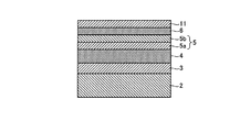
図1は、本発明の実施の形態1に係る半導体素子である半導体レーザ素子の模式的な断面図である。図1に示すように、この半導体レーザ素子100は、裏面にn側電極1が形成された、n型InPからなる基板2と、基板2上に順次形成された、n型InPからなる下部クラッド層3と、AlGaInAsからなる活性層4と、p型InPからなる下部ブロッキング層5aとn型InPからなる上部ブロッキング層5bとからなる2つの電流ブロッキング層5と、p型AlInAsからなる2つのエッチ停止層6とを備えている。
(Embodiment 1)
FIG. 1 is a schematic cross-sectional view of a semiconductor laser element that is a semiconductor element according to
エッチ停止層6は2つに分離しており、その間には紙面に対して垂直方向に延伸している開口パターンが形成されている。2つの電流ブロッキング層5およびエッチ停止層6の間には、活性層4の上面を底面として、エッチ停止層6の開口パターンの形状に一致するように紙面に対して垂直方向に延伸しているストライプ溝Gが形成されている。ストライプ溝Gの幅はたとえば3μmであるが、半導体レーザ素子100のレーザ発振波長の光をシングルモードで導波できるように幅を適宜設定する。
The
さらに、この半導体レーザ素子100は、エッチ停止層6の表面からストライプ溝Gの内表面にわたって形成されたp型GaInAsPからなる光導波路層7と、光導波路層7上に形成されたp型InPからなる上部クラッド層8と、上部クラッド層8上に順次形成された、p型GaInAsからなるコンタクト層9と、p側電極10とを備えている。また、紙面と平行に形成された半導体レーザ素子100の端面には、光共振器を形成するための反射膜が形成されている。
Further, the
活性層4は、たとえば、交互に積層した井戸層と障壁層とからなる多重量子井戸(MQW:Multi Quantum Well)層の上下に分離閉じ込めヘテロ構造(SCH:Separate Confinement Heterostructure)層を形成したMQW−SCH構造を有する。ただし、活性層4の構造は特に限定されず、SCH層を備えなくてもよいし、単一量子井戸構造やバルク構造でもよい。また、活性層4がAlGaInAsからなることによって、1.3μm帯のレーザ発振を実現できる。なお、活性層4の組成は所望のレーザ発振波長に応じて適宜設定される。
The
この半導体レーザ素子100は、2つの電流ブロッキング層5間のストライプ溝G内に、光導波路層7および上部クラッド層8による活性層4に対する電流注入のためのチャネルが形成された、いわゆるSAS(Self Aligned Structure)構造を有するものである。したがって、この半導体レーザ素子100は、電流キャリアおよび光をチャネル内に有効に閉じ込めることができるので、低しきい値電流、高効率でのレーザ発振を実現することができる。
In this
また、この半導体レーザ素子100は、活性層4がAlGaInAsからなるため、高温においても電子キャリアのリークが少ないので温度特性に優れており、かつホールキャリアの移動度が高いので高速変調特性にも優れている。
In addition, since the
また、この半導体レーザ素子100は、電流ブロッキング層5とエッチ停止層6とによってpnp接合が実現されており、急峻なpn界面が形成されるため、電流ブロッキング特性に優れているため、さらに高効率のレーザ素子となる。
In addition, since the
さらに、この半導体レーザ素子100は、以下に説明するように、ストライプ溝Gが、Al系化合物半導体層であるエッチ停止層6をエッチングマスクとして、Al系化合物半導体層である活性層4をエッチ停止層としてエッチングすることによって形成されているので、従来よりも簡易な製造工程で生産性および製造歩留まり高く製造された低コストのものである。
Further, in the
(製造方法)
つぎに、半導体レーザ素子100の製造方法について説明する。図2〜図5は、図1に示す半導体レーザ素子100の製造方法を説明する図である。
(Production method)
Next, a method for manufacturing the
はじめに、基板2をMOCVD(有機金属気相成長)装置などの半導体結晶成長装置に導入し、図2に示すように、基板2上に、下部クラッド層3、活性層4、下部ブロッキング層5aと上部ブロッキング層5bとからなる電流ブロッキング層5、およびエッチ停止層6を順次形成し、さらにエッチ停止層6上にp型InPからなる保護層11を形成する。
First, the
つぎに、基板2を半導体結晶成長装置から取り出す。このとき、Al系化合物半導体層であるエッチ停止層6は、保護層11によって保護されているので、大気に曝されて酸化することが防止される。その結果、後にエッチ停止層6の上に形成する半導体層の結晶性が良好になる。
Next, the
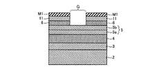
つぎに、取り出した基板2をプラズマCVD装置に導入し、SiNx膜を全面に形成した後、フォトリソグラフィーの手法およびCF4系ガスを用いたドライエッチングによって、SiNx膜にストライプ溝Gの形状の開口パターンを形成してマスクM1とし、さらにウエットエッチングまたはドライエッチングによってマスクM1の開口パターン内のエッチ停止層6および保護層11を除去し、ストライプ溝Gを形成する(図3参照)。その後マスクM1は除去する。
Next, after the taken-out
つぎに、基板2を再び半導体結晶成長装置に導入し、臭素系ガスであるCBr4ガスを用いたエッチングによって保護層11およびストライプ溝G内の電流ブロッキング層5を除去する(図4参照)。このエッチング工程は、たとえばエッチング温度を600℃とし、PH3雰囲気においてCBr4ガスを3μmol/minで供給することによりなされる。この場合のエッチングレートは20nm/minとなる。
Next, the
ここで、CBr4ガスは、InPからなる保護層11および電流ブロッキング層5をエッチングするが、Al系化合物半導体層である活性層4およびエッチ停止層6をエッチングしない。そのため、ストライプ溝G外ではエッチ停止層6の上面において、またストライプ溝G内では活性層4の上面において、エッチングを停止させることができる。すなわち、活性層4はエッチ停止層としても機能する。その結果、ストライプ溝Gの底面は活性層4の上面の深さにまで到達する。
Here, the CBr 4 gas etches the
このエッチング工程に続いて、図5に示すように、半導体結晶成長装置内にて、ストライプ溝G内に光導波路層7と上部クラッド層8とを形成し、さらにコンタクト層9を形成する。最後に、コンタクト層9の上面にp側電極10を形成し、基板2が所望の厚さになるように裏面を研磨した後にn側電極1を形成し、へき開による端面の形成および端面に反射膜の形成を行い、素子分離して半導体レーザ素子100が完成する。
Following this etching step, as shown in FIG. 5, the
このように、本製造方法では、エッチング工程の後に、基板2を半導体結晶成長装置から取り出さずにそのまま続けて、残りの半導体層の形成を行うことができる。その結果、半導体結晶成長装置からの取り出しが1度ですみ、製造工程が簡略化されるので、半導体レーザ素子100の生産性が高くなるとともに、取り出した際に基板2が汚染されるおそれが少なくなるので、製造歩留まりが高くなる。また、エッチング工程においてストライプ溝G内に活性層4の一部表面が露出するが、この表面がその後大気に曝されることがないので、酸化されるおそれもない。その結果、活性層4の上に形成する半導体層の結晶性が良好になるので、信頼性に優れた半導体レーザ素子100を実現できる。
Thus, in this manufacturing method, after the etching process, the
さらに、エッチング工程において、エッチング深さの制御性が高いCBr4ガスによるエッチングを行っているため、半導体レーザ素子100のレーザ特性の面内均一性が高くなる。さらに、従来技術とは異なり、SiNx膜を用いて選択エッチングや選択成長を行わないので、半導体層とは熱膨張係数が異なるSiNxによって半導体層に熱応力によるダメージが加わるということがない。また、SiNx膜の除去の際のドライエッチングによるダメージも加わるということがない。したがって、これらのダメージによる半導体レーザ素子100の信頼性の低下を防止できる。
Further, in the etching process, etching with CBr 4 gas having high controllability of the etching depth is performed, so that the in-plane uniformity of the laser characteristics of the
なお、CBr4ガスを用いた場合にInP半導体層に対して活性層4およびエッチ停止層6をエッチ停止層として機能させるためには、活性層4およびエッチ停止層6にAlが含まれていることが重要である。活性層4およびエッチ停止層6のAl組成は大きければ大きいほど好ましいが、たとえば5%以上である。また、Al組成の上限はたとえば48%である。
In order to make the
以上説明したように、本製造方法によれば、生産性および製造歩留まりを高く半導体レーザ素子100を製造でき、低コストの半導体レーザ素子100を実現できる。
As described above, according to the present manufacturing method, the
(実施の形態2)
つぎに、本発明の実施の形態2について説明する。上記実施の形態1に係る半導体レーザ素子では、Al系化合物半導体層である活性層をエッチ停止層として用いたが、本実施の形態2に係る半導体レーザ素子では、活性層の上方に活性層とは別個にエッチ停止層を備えた構造を有している。
(Embodiment 2)
Next, a second embodiment of the present invention will be described. In the semiconductor laser device according to the first embodiment, the active layer that is an Al-based compound semiconductor layer is used as the etch stop layer. However, in the semiconductor laser device according to the second embodiment, the active layer and the active layer are disposed above the active layer. Has a structure with a separate etch stop layer.
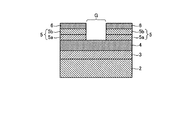
図6は、本実施の形態2に係る半導体レーザ素子の模式的な断面図である。図6に示すように、この半導体レーザ素子200は、裏面にn側電極1が形成された基板2と基板2上に順次形成された、下部クラッド層3と、GaInAsPからなる活性層12と、p型AlInAsからなるエッチ停止層13と、下部ブロッキング層5aと上部ブロッキング層5bとからなる2つの電流ブロッキング層5と、2つのエッチ停止層6とを備えている。
FIG. 6 is a schematic cross-sectional view of the semiconductor laser device according to the second embodiment. As shown in FIG. 6, the
エッチ停止層6は2つに分離しており、その間には紙面に対して垂直方向に延伸している開口パターンが形成されている。2つの電流ブロッキング層5およびエッチ停止層6の間には、エッチ停止層13の上面を底面として、エッチ停止層6の開口パターンの形状に一致するように紙面に対して垂直方向に延伸しているストライプ溝Gが形成されている。さらに、この半導体レーザ素子200は、エッチ停止層6の表面からストライプ溝Gの内表面にわたって形成された光導波路層7と、光導波路層7上に形成された上部クラッド層8と、上部クラッド層8上に順次形成された、コンタクト層9とp側電極10とを備えている。また、紙面と平行に形成された半導体レーザ素子200の端面には、光共振器を形成するための反射膜が形成されている。
The
すなわち、図1に示す半導体レーザ素子100と半導体レーザ素子200とを比較すると、半導体レーザ素子200は活性層12がGaInAsPからなり、活性層12の上にp型AlInAsからなるエッチ停止層13を備える点が異なる。
That is, when comparing the
この半導体レーザ素子200も半導体レーザ素子100と同様に、SAS構造を有し、電流ブロッキング層5とエッチ停止層6とによってpnp接合が実現されている。したがって、半導体レーザ素子200は、低しきい値電流、高効率でのレーザ発振を実現することができ、電流ブロッキング特性に優れているためにさらに高効率のレーザ素子となる。なお、活性層12がGaInAsPからなることによって、1.3〜1.6μm帯のレーザ発振を実現できる。活性層12の組成は所望のレーザ発振波長に応じて適宜設定される。また、活性層12は活性層4と同様にMQW−SCH構造を有するが、特に限定されない。
Similar to the
さらに、この半導体レーザ素子200は、ストライプ溝Gが、Al系化合物半導体層であるエッチ停止層6をエッチングマスクとして、Al系化合物半導体層であるエッチ停止層13をエッチ停止層としてエッチングすることによって形成されている。したがって、半導体レーザ素子100と同様に、従来よりも簡易な製造工程で生産性および製造歩留まり高く製造された低コストのものである。
Further, in the
(製造方法)
つぎに、半導体レーザ素子200の製造方法について説明する。図7〜図8は、図1に示す半導体レーザ素子200の製造方法を説明する図である。
(Production method)
Next, a method for manufacturing the
はじめに、半導体レーザ素子100の場合と同様に、基板2をMOCVD装置などの半導体結晶成長装置に導入し、基板2上に、下部クラッド層3、活性層12、エッチ停止層13、下部ブロッキング層5aと上部ブロッキング層5bとからなる電流ブロッキング層5、およびエッチ停止層6を順次形成し、さらにエッチ停止層6上にp型InPからなる保護層11を形成する。つぎに、基板2を半導体結晶成長装置から取り出す。
First, as in the case of the
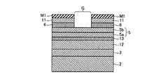
つぎに、取り出した基板2をプラズマCVD装置に導入し、半導体レーザ素子100の場合と同様にマスクM1を形成し、さらにウエットエッチングまたはドライエッチングによってマスクM1の開口パターン内のエッチ停止層6および保護層11を除去し、ストライプ溝Gを形成する(図7参照)。その後マスクM1は除去する。
Next, the taken-out
つぎに、基板2を再び半導体結晶成長装置に導入し、CBr4ガスを用いたエッチングによって保護層11およびストライプ溝G内の電流ブロッキング層5を除去する(図8参照)。このとき、ストライプ溝G外ではエッチ停止層6の上面において、またストライプ溝G内ではエッチ停止層13の上面において、エッチングを停止させることができる。
Next, the
このエッチング工程に続いて、半導体レーザ素子100の場合と同様に、半導体結晶成長装置内にて、光導波路層7と、上部クラッド層8と、コンタクト層9とを順次形成する。最後に、コンタクト層9の上面にp側電極10を形成し、基板2が所望の厚さになるように裏面を研磨した後にn側電極1を形成し、へき開による端面の形成および端面に反射膜の形成を行い、素子分離して半導体レーザ素子200が完成する。
Following this etching step, as in the case of the
このように、本製造方法においても、半導体レーザ素子100の場合と同様に、半導体レーザ素子200の生産性が高くなるとともに、製造歩留まりが高くなる。また、エッチング工程においてストライプ溝G内に露出したエッチ停止層13の表面がその後大気に曝されないので、酸化されるおそれもない。その結果、エッチ停止層13の上に形成する半導体層の結晶性が良好になるので、信頼性に優れた半導体レーザ素子200を実現できる。さらには、半導体レーザ素子200のレーザ特性の面内均一性が高くなる。
As described above, also in this manufacturing method, as in the case of the
なお、CBr4ガスを用いた場合にInP半導体層に対してエッチ停止層13をエッチ停止層として機能させるためには、エッチ停止層13にAlが含まれていることが重要である。エッチ停止層13のAl組成は大きければ大きいほど好ましいが、たとえば5%以上が好ましく、上限はたとえば48%である。
In addition, when the CBr 4 gas is used, in order for the
以上説明したように、本製造方法によれば、生産性および製造歩留まりを高く半導体レーザ素子200を製造でき、低コストの半導体レーザ素子200を実現できる。
As described above, according to the present manufacturing method, the
なお、本実施の形態2に係る半導体レーザ素子200は、活性層12がGaInAsPからなるが、この活性層12は半導体レーザ素子100と同様のAlGaInAsからなる活性層に置き換えてもよい。
In the
また、本実施の形態2に係る半導体レーザ素子200では、活性層12の直上にエッチ停止層13が形成されているが、活性層12とエッチ停止層13との間に別の半導体層を介挿させてもよい。
In the
また、上記実施の形態1では、活性層4全体がAl系化合物半導体からなるが、たとえば少なくとも活性層4上部のSCH層をAl系化合物半導体で構成し、MQW層はたとえばAlを含まないGaInAsPで構成してもよい。
In the first embodiment, the entire
また、上記実施の形態では、ストライプ溝形成のためのエッチングガスとしてCBr4ガスを用いているが、たとえばCH3Br等の他の臭素系ガスを用いてもよい。 In the above embodiment, CBr 4 gas is used as the etching gas for forming the stripe groove, but other bromine-based gas such as CH 3 Br may be used.
また、上記実施の形態では、Al系化合物半導体層によってエッチングを停止させるようにしてエッチングする半導体層は、InPからなる。しかしながら、エッチングする半導体層はInPに限らず、使用する臭素系ガスに対してAl系化合物半導体層とのエッチング選択比が十分に大きい(たとえば10以上、さらに好ましくは1000以上)材料からなる半導体層であればよい。したがって、たとえばGaInAsPなどのAlを含まずにリン(P)を含むIII−V族化合物半導体層(P系化合物半導体層)からなる半導体層や、Alを含まずにIn、Ga、As、およびPの少なくとも2つを含むIII−V族化合物半導体層からなる半導体層でもよい。 Moreover, in the said embodiment, the semiconductor layer etched so that etching may be stopped with an Al type compound semiconductor layer consists of InP. However, the semiconductor layer to be etched is not limited to InP, but a semiconductor layer made of a material having a sufficiently high etching selection ratio with the Al-based compound semiconductor layer with respect to the bromine-based gas used (for example, 10 or more, more preferably 1000 or more). If it is. Therefore, for example, a semiconductor layer composed of a III-V compound semiconductor layer (P-based compound semiconductor layer) containing phosphorus (P) without containing Al, such as GaInAsP, or In, Ga, As, and P containing no Al. The semiconductor layer which consists of a III-V group compound semiconductor layer containing at least 2 of these may be sufficient.
また、上記実施の形態では、InPからなる基板を使用しているが、GaAsからなる基板を使用してもよい。この場合、エッチングを停止させるAl系化合物半導体層としてはAlGaAsからなるものを使用することができる。また、エッチングするP系化合物半導体層としてはGaInPまたはGaInAsPからなるものを使用することができる。 Moreover, in the said embodiment, although the board | substrate which consists of InP is used, you may use the board | substrate which consists of GaAs. In this case, an Al-based compound semiconductor layer for stopping etching can be made of AlGaAs. Further, as the P-based compound semiconductor layer to be etched, a layer made of GaInP or GaInAsP can be used.
また、上記実施の形態は、SAS構造の半導体レーザ素子に対して本発明を適用したものである。しかしながら、本発明の適用範囲は特に限定されず、たとえばバットジョイント成長を行う場合のように、半導体積層構造に所定の形状を有する溝を形成し、その溝内に別の半導体層を成長した構造を有するあらゆる半導体素子に適用することができる。 In the above embodiment, the present invention is applied to a semiconductor laser element having a SAS structure. However, the scope of application of the present invention is not particularly limited. For example, a structure in which a groove having a predetermined shape is formed in a semiconductor multilayer structure and another semiconductor layer is grown in the groove, as in the case of performing butt joint growth. It can be applied to any semiconductor device having
また、上記実施の形態により本発明が限定されるものではない。上述した各構成要素を適宜組み合わせて構成したものも本発明に含まれる。その他、上記実施の形態に基づいて当業者等によりなされる他の実施の形態、実施例及び運用技術等は全て本発明に含まれる。 Further, the present invention is not limited by the above embodiment. What was comprised combining each component mentioned above suitably is also contained in this invention. In addition, other embodiments, examples, operational techniques, and the like made by those skilled in the art based on the above-described embodiments are all included in the present invention.
1 n側電極
2 基板
3 下部クラッド層
4、12 活性層
5 電流ブロッキング層
5a 下部ブロッキング層
5b 上部ブロッキング層
6、13 エッチ停止層
7 光導波路層
8 上部クラッド層
9 コンタクト層
10 p側電極
11 保護層
100、200 半導体レーザ素子
G ストライプ溝
M1 マスク
1 n-
Claims (13)
前記第1の半導体層をエッチ停止層として、前記所定のエッチングガスにて前記第2の半導体層の開口パターンの下の前記第3の半導体層をエッチング除去するエッチング工程と、
前記エッチング工程によって前記第3の半導体層に形成された溝内に第4の半導体層を形成する半導体層形成工程と、
を含むことを特徴とする半導体素子の製造方法。 A first semiconductor layer made of a group III-V compound semiconductor containing aluminum, and a second semiconductor made of a group III-V compound semiconductor containing aluminum and located above the first semiconductor layer and having an opening pattern And a material having a high etching selectivity with respect to the first and second semiconductor layers when a predetermined etching gas is used, and located between the first semiconductor layer and the second semiconductor layer. A semiconductor multilayer structure forming step of forming a semiconductor multilayer structure including a third semiconductor layer on the substrate;
An etching step of etching and removing the third semiconductor layer under the opening pattern of the second semiconductor layer with the predetermined etching gas using the first semiconductor layer as an etch stop layer;
A semiconductor layer forming step of forming a fourth semiconductor layer in a groove formed in the third semiconductor layer by the etching step;
The manufacturing method of the semiconductor element characterized by the above-mentioned.
前記エッチング工程において、前記第2の半導体層をエッチ停止層として、前記所定のエッチングガスにて前記第5の半導体層をエッチング除去することを特徴とする請求項1に記載の半導体素子の製造方法。 The semiconductor multilayer structure forming step includes a step of forming a fifth semiconductor layer made of a material having a high etching selectivity with respect to the first and second semiconductor layers on the second semiconductor layer,
2. The method of manufacturing a semiconductor device according to claim 1, wherein, in the etching step, the fifth semiconductor layer is etched away with the predetermined etching gas using the second semiconductor layer as an etch stop layer. 3. .
前記基板上に形成されたアルミニウムを含むIII−V族化合物半導体からなる第1の半導体層と、
アルミニウムを含むIII−V族化合物半導体からなり、前記第1の半導体層の上方に位置し、開口パターンを有する第2の半導体層と、
前記第1の半導体層と前記第2の半導体層との間に位置し、該第2の半導体層の開口パターンの形状に一致した溝を有し、所定のエッチングガスを用いる場合に該第1および第2の半導体層に対してエッチング選択比が大きい材料からなる第3の半導体層と、
少なくとも前記第3の半導体層の溝内に形成された第4の半導体層と、
を備えることを特徴とする半導体素子。 A substrate,
A first semiconductor layer made of a group III-V compound semiconductor containing aluminum formed on the substrate;
A second semiconductor layer comprising an III-V group compound semiconductor containing aluminum, located above the first semiconductor layer and having an opening pattern;
The first semiconductor layer has a groove located between the first semiconductor layer and the second semiconductor layer, and has a groove that matches the shape of the opening pattern of the second semiconductor layer. When a predetermined etching gas is used, the first semiconductor layer is used. And a third semiconductor layer made of a material having a high etching selectivity with respect to the second semiconductor layer,
A fourth semiconductor layer formed at least in the trench of the third semiconductor layer;
A semiconductor device comprising:
Priority Applications (1)
| Application Number | Priority Date | Filing Date | Title |
|---|---|---|---|
| JP2011031008A JP2012169540A (en) | 2011-02-16 | 2011-02-16 | Semiconductor element manufacturing method and semiconductor element |
Applications Claiming Priority (1)
| Application Number | Priority Date | Filing Date | Title |
|---|---|---|---|
| JP2011031008A JP2012169540A (en) | 2011-02-16 | 2011-02-16 | Semiconductor element manufacturing method and semiconductor element |
Publications (1)
| Publication Number | Publication Date |
|---|---|
| JP2012169540A true JP2012169540A (en) | 2012-09-06 |
Family
ID=46973392
Family Applications (1)
| Application Number | Title | Priority Date | Filing Date |
|---|---|---|---|
| JP2011031008A Pending JP2012169540A (en) | 2011-02-16 | 2011-02-16 | Semiconductor element manufacturing method and semiconductor element |
Country Status (1)
| Country | Link |
|---|---|
| JP (1) | JP2012169540A (en) |
Citations (4)
| Publication number | Priority date | Publication date | Assignee | Title |
|---|---|---|---|---|
| JPS6220323A (en) * | 1985-07-18 | 1987-01-28 | Nec Corp | Manufacture of semiconductor device |
| JPH0536655A (en) * | 1991-07-25 | 1993-02-12 | Nec Corp | Method for working compound semiconductor |
| JPH0684805A (en) * | 1992-09-01 | 1994-03-25 | Fujitsu Ltd | Compound semiconductor crystalline growth method |
| JP2002118327A (en) * | 2000-10-06 | 2002-04-19 | Furukawa Electric Co Ltd:The | Method for manufacturing compound semiconductor device |
-
2011
- 2011-02-16 JP JP2011031008A patent/JP2012169540A/en active Pending
Patent Citations (4)
| Publication number | Priority date | Publication date | Assignee | Title |
|---|---|---|---|---|
| JPS6220323A (en) * | 1985-07-18 | 1987-01-28 | Nec Corp | Manufacture of semiconductor device |
| JPH0536655A (en) * | 1991-07-25 | 1993-02-12 | Nec Corp | Method for working compound semiconductor |
| JPH0684805A (en) * | 1992-09-01 | 1994-03-25 | Fujitsu Ltd | Compound semiconductor crystalline growth method |
| JP2002118327A (en) * | 2000-10-06 | 2002-04-19 | Furukawa Electric Co Ltd:The | Method for manufacturing compound semiconductor device |
Similar Documents
| Publication | Publication Date | Title |
|---|---|---|
| JP2008053501A (en) | Integrated optical device, and its manufacturing method | |
| JP5247444B2 (en) | Semiconductor laser device | |
| JP2000216492A (en) | Semiconductor light element, its manufacture, and semiconductor optical device | |
| US9257815B1 (en) | Optical semiconductor device | |
| US11710941B2 (en) | Semiconductor laser element | |
| JP2016134522A (en) | Optical semiconductor device | |
| KR100912564B1 (en) | Semiconductor optical device and manufacturing method therefor | |
| JP2009117539A (en) | Optical semiconductor element, and manufacturing method of optical semiconductor element | |
| JP2005286192A (en) | Optically integrated device | |
| JP5273459B2 (en) | Manufacturing method of semiconductor laser | |
| JP2006093682A (en) | Semiconductor laser and method of manufacturing the same | |
| US20150043604A1 (en) | Semiconductor light emitting device and method for manufacturing same | |
| JP2008098387A (en) | Method of manufacturing diffraction grating | |
| JP4984514B2 (en) | Semiconductor light emitting device and method for manufacturing the semiconductor light emitting device | |
| JP2012169540A (en) | Semiconductor element manufacturing method and semiconductor element | |
| JP2005317572A (en) | Semiconductor device and manufacturing method thereof | |
| JP4983791B2 (en) | Optical semiconductor element | |
| JP2009105458A (en) | Optical semiconductor device | |
| JP2000077780A (en) | Semiconductor laser and manufacture thereof | |
| JP2008022043A (en) | Method of manufacturing semiconductor laser device | |
| JP5610032B2 (en) | Manufacturing method of semiconductor laser | |
| JP2006216752A (en) | Manufacturing method for diffraction grating and semiconductor laser | |
| JP2009099844A (en) | Gain coupling type distributed feedback type semiconductor laser apparatus | |
| JP5257296B2 (en) | Optical semiconductor device and method for manufacturing optical semiconductor device | |
| JP2013048165A (en) | Optical integrated device and manufacturing method of the same |
Legal Events
| Date | Code | Title | Description |
|---|---|---|---|
| A621 | Written request for application examination |
Free format text: JAPANESE INTERMEDIATE CODE: A621 Effective date: 20140204 |
|
| A977 | Report on retrieval |
Free format text: JAPANESE INTERMEDIATE CODE: A971007 Effective date: 20140528 |
|
| A131 | Notification of reasons for refusal |
Free format text: JAPANESE INTERMEDIATE CODE: A131 Effective date: 20140603 |
|
| A02 | Decision of refusal |
Free format text: JAPANESE INTERMEDIATE CODE: A02 Effective date: 20141111 |