EP1195811A1 - Semiconductor device - Google Patents
Semiconductor device Download PDFInfo
- Publication number
- EP1195811A1 EP1195811A1 EP00905287A EP00905287A EP1195811A1 EP 1195811 A1 EP1195811 A1 EP 1195811A1 EP 00905287 A EP00905287 A EP 00905287A EP 00905287 A EP00905287 A EP 00905287A EP 1195811 A1 EP1195811 A1 EP 1195811A1
- Authority
- EP
- European Patent Office
- Prior art keywords
- group
- semiconductor device
- polyamide
- resin composition
- photosensitive resin
- Prior art date
- Legal status (The legal status is an assumption and is not a legal conclusion. Google has not performed a legal analysis and makes no representation as to the accuracy of the status listed.)
- Granted
Links
- 0 Cc(cc1)ccc1N(C*(*)*C1CC1)NC Chemical compound Cc(cc1)ccc1N(C*(*)*C1CC1)NC 0.000 description 10
- JGUGUGNTNRJZJI-UHFFFAOYSA-N CC(c(cc(C)cc1)c1O)c1cc(C)ccc1O Chemical compound CC(c(cc(C)cc1)c1O)c1cc(C)ccc1O JGUGUGNTNRJZJI-UHFFFAOYSA-N 0.000 description 1
- VOWZNBNDMFLQGM-UHFFFAOYSA-N Cc1cc(N)c(C)cc1 Chemical compound Cc1cc(N)c(C)cc1 VOWZNBNDMFLQGM-UHFFFAOYSA-N 0.000 description 1
Images


Classifications
-
- G—PHYSICS
- G03—PHOTOGRAPHY; CINEMATOGRAPHY; ANALOGOUS TECHNIQUES USING WAVES OTHER THAN OPTICAL WAVES; ELECTROGRAPHY; HOLOGRAPHY
- G03F—PHOTOMECHANICAL PRODUCTION OF TEXTURED OR PATTERNED SURFACES, e.g. FOR PRINTING, FOR PROCESSING OF SEMICONDUCTOR DEVICES; MATERIALS THEREFOR; ORIGINALS THEREFOR; APPARATUS SPECIALLY ADAPTED THEREFOR
- G03F7/00—Photomechanical, e.g. photolithographic, production of textured or patterned surfaces, e.g. printing surfaces; Materials therefor, e.g. comprising photoresists; Apparatus specially adapted therefor
- G03F7/004—Photosensitive materials
- G03F7/038—Macromolecular compounds which are rendered insoluble or differentially wettable
-
- C—CHEMISTRY; METALLURGY
- C08—ORGANIC MACROMOLECULAR COMPOUNDS; THEIR PREPARATION OR CHEMICAL WORKING-UP; COMPOSITIONS BASED THEREON
- C08G—MACROMOLECULAR COMPOUNDS OBTAINED OTHERWISE THAN BY REACTIONS ONLY INVOLVING UNSATURATED CARBON-TO-CARBON BONDS
- C08G73/00—Macromolecular compounds obtained by reactions forming a linkage containing nitrogen with or without oxygen or carbon in the main chain of the macromolecule, not provided for in groups C08G12/00 - C08G71/00
- C08G73/06—Polycondensates having nitrogen-containing heterocyclic rings in the main chain of the macromolecule
- C08G73/22—Polybenzoxazoles
-
- C—CHEMISTRY; METALLURGY
- C09—DYES; PAINTS; POLISHES; NATURAL RESINS; ADHESIVES; COMPOSITIONS NOT OTHERWISE PROVIDED FOR; APPLICATIONS OF MATERIALS NOT OTHERWISE PROVIDED FOR
- C09D—COATING COMPOSITIONS, e.g. PAINTS, VARNISHES OR LACQUERS; FILLING PASTES; CHEMICAL PAINT OR INK REMOVERS; INKS; CORRECTING FLUIDS; WOODSTAINS; PASTES OR SOLIDS FOR COLOURING OR PRINTING; USE OF MATERIALS THEREFOR
- C09D179/00—Coating compositions based on macromolecular compounds obtained by reactions forming in the main chain of the macromolecule a linkage containing nitrogen, with or without oxygen, or carbon only, not provided for in groups C09D161/00 - C09D177/00
- C09D179/04—Polycondensates having nitrogen-containing heterocyclic rings in the main chain; Polyhydrazides; Polyamide acids or similar polyimide precursors
-
- G—PHYSICS
- G03—PHOTOGRAPHY; CINEMATOGRAPHY; ANALOGOUS TECHNIQUES USING WAVES OTHER THAN OPTICAL WAVES; ELECTROGRAPHY; HOLOGRAPHY
- G03F—PHOTOMECHANICAL PRODUCTION OF TEXTURED OR PATTERNED SURFACES, e.g. FOR PRINTING, FOR PROCESSING OF SEMICONDUCTOR DEVICES; MATERIALS THEREFOR; ORIGINALS THEREFOR; APPARATUS SPECIALLY ADAPTED THEREFOR
- G03F7/00—Photomechanical, e.g. photolithographic, production of textured or patterned surfaces, e.g. printing surfaces; Materials therefor, e.g. comprising photoresists; Apparatus specially adapted therefor
- G03F7/004—Photosensitive materials
- G03F7/022—Quinonediazides
- G03F7/023—Macromolecular quinonediazides; Macromolecular additives, e.g. binders
- G03F7/0233—Macromolecular quinonediazides; Macromolecular additives, e.g. binders characterised by the polymeric binders or the macromolecular additives other than the macromolecular quinonediazides
-
- H—ELECTRICITY
- H10—SEMICONDUCTOR DEVICES; ELECTRIC SOLID-STATE DEVICES NOT OTHERWISE PROVIDED FOR
- H10W—GENERIC PACKAGES, INTERCONNECTIONS, CONNECTORS OR OTHER CONSTRUCTIONAL DETAILS OF DEVICES COVERED BY CLASS H10
- H10W20/00—Interconnections in chips, wafers or substrates
- H10W20/40—Interconnections external to wafers or substrates, e.g. back-end-of-line [BEOL] metallisations or vias connecting to gate electrodes
- H10W20/45—Interconnections external to wafers or substrates, e.g. back-end-of-line [BEOL] metallisations or vias connecting to gate electrodes characterised by their insulating parts
- H10W20/48—Insulating materials thereof
-
- H—ELECTRICITY
- H10—SEMICONDUCTOR DEVICES; ELECTRIC SOLID-STATE DEVICES NOT OTHERWISE PROVIDED FOR
- H10W—GENERIC PACKAGES, INTERCONNECTIONS, CONNECTORS OR OTHER CONSTRUCTIONAL DETAILS OF DEVICES COVERED BY CLASS H10
- H10W70/00—Package substrates; Interposers; Redistribution layers [RDL]
- H10W70/01—Manufacture or treatment
- H10W70/05—Manufacture or treatment of insulating or insulated package substrates, or of interposers, or of redistribution layers
-
- H—ELECTRICITY
- H10—SEMICONDUCTOR DEVICES; ELECTRIC SOLID-STATE DEVICES NOT OTHERWISE PROVIDED FOR
- H10W—GENERIC PACKAGES, INTERCONNECTIONS, CONNECTORS OR OTHER CONSTRUCTIONAL DETAILS OF DEVICES COVERED BY CLASS H10
- H10W72/00—Interconnections or connectors in packages
- H10W72/01—Manufacture or treatment
- H10W72/012—Manufacture or treatment of bump connectors, dummy bumps or thermal bumps
-
- H—ELECTRICITY
- H10—SEMICONDUCTOR DEVICES; ELECTRIC SOLID-STATE DEVICES NOT OTHERWISE PROVIDED FOR
- H10W—GENERIC PACKAGES, INTERCONNECTIONS, CONNECTORS OR OTHER CONSTRUCTIONAL DETAILS OF DEVICES COVERED BY CLASS H10
- H10W72/00—Interconnections or connectors in packages
- H10W72/01—Manufacture or treatment
- H10W72/012—Manufacture or treatment of bump connectors, dummy bumps or thermal bumps
- H10W72/01251—Changing the shapes of bumps
- H10W72/01255—Changing the shapes of bumps by using masks
-
- H—ELECTRICITY
- H10—SEMICONDUCTOR DEVICES; ELECTRIC SOLID-STATE DEVICES NOT OTHERWISE PROVIDED FOR
- H10W—GENERIC PACKAGES, INTERCONNECTIONS, CONNECTORS OR OTHER CONSTRUCTIONAL DETAILS OF DEVICES COVERED BY CLASS H10
- H10W72/00—Interconnections or connectors in packages
- H10W72/20—Bump connectors, e.g. solder bumps or copper pillars; Dummy bumps; Thermal bumps
-
- H—ELECTRICITY
- H10—SEMICONDUCTOR DEVICES; ELECTRIC SOLID-STATE DEVICES NOT OTHERWISE PROVIDED FOR
- H10W—GENERIC PACKAGES, INTERCONNECTIONS, CONNECTORS OR OTHER CONSTRUCTIONAL DETAILS OF DEVICES COVERED BY CLASS H10
- H10W72/00—Interconnections or connectors in packages
- H10W72/20—Bump connectors, e.g. solder bumps or copper pillars; Dummy bumps; Thermal bumps
- H10W72/241—Dispositions, e.g. layouts
- H10W72/244—Dispositions, e.g. layouts relative to underlying supporting features, e.g. bond pads, RDLs or vias
-
- H—ELECTRICITY
- H10—SEMICONDUCTOR DEVICES; ELECTRIC SOLID-STATE DEVICES NOT OTHERWISE PROVIDED FOR
- H10W—GENERIC PACKAGES, INTERCONNECTIONS, CONNECTORS OR OTHER CONSTRUCTIONAL DETAILS OF DEVICES COVERED BY CLASS H10
- H10W72/00—Interconnections or connectors in packages
- H10W72/20—Bump connectors, e.g. solder bumps or copper pillars; Dummy bumps; Thermal bumps
- H10W72/251—Materials
-
- H—ELECTRICITY
- H10—SEMICONDUCTOR DEVICES; ELECTRIC SOLID-STATE DEVICES NOT OTHERWISE PROVIDED FOR
- H10W—GENERIC PACKAGES, INTERCONNECTIONS, CONNECTORS OR OTHER CONSTRUCTIONAL DETAILS OF DEVICES COVERED BY CLASS H10
- H10W72/00—Interconnections or connectors in packages
- H10W72/20—Bump connectors, e.g. solder bumps or copper pillars; Dummy bumps; Thermal bumps
- H10W72/29—Bond pads specially adapted therefor
-
- H—ELECTRICITY
- H10—SEMICONDUCTOR DEVICES; ELECTRIC SOLID-STATE DEVICES NOT OTHERWISE PROVIDED FOR
- H10W—GENERIC PACKAGES, INTERCONNECTIONS, CONNECTORS OR OTHER CONSTRUCTIONAL DETAILS OF DEVICES COVERED BY CLASS H10
- H10W72/00—Interconnections or connectors in packages
- H10W72/90—Bond pads, in general
- H10W72/921—Structures or relative sizes of bond pads
- H10W72/923—Bond pads having multiple stacked layers
-
- H—ELECTRICITY
- H10—SEMICONDUCTOR DEVICES; ELECTRIC SOLID-STATE DEVICES NOT OTHERWISE PROVIDED FOR
- H10W—GENERIC PACKAGES, INTERCONNECTIONS, CONNECTORS OR OTHER CONSTRUCTIONAL DETAILS OF DEVICES COVERED BY CLASS H10
- H10W72/00—Interconnections or connectors in packages
- H10W72/90—Bond pads, in general
- H10W72/941—Dispositions of bond pads
- H10W72/942—Dispositions of bond pads relative to underlying supporting features, e.g. bond pads, RDLs or vias
-
- H—ELECTRICITY
- H10—SEMICONDUCTOR DEVICES; ELECTRIC SOLID-STATE DEVICES NOT OTHERWISE PROVIDED FOR
- H10W—GENERIC PACKAGES, INTERCONNECTIONS, CONNECTORS OR OTHER CONSTRUCTIONAL DETAILS OF DEVICES COVERED BY CLASS H10
- H10W72/00—Interconnections or connectors in packages
- H10W72/90—Bond pads, in general
- H10W72/951—Materials of bond pads
- H10W72/952—Materials of bond pads comprising metals or metalloids, e.g. PbSn, Ag or Cu
Definitions
- the present invention relates to a semiconductor device having a positive photosensitive resin composition of high sensitivity, capable of giving a pattern of high residual film ratio and provided with a bump electrode.
- an inorganic film e.g. SiO 2 film or SiN film
- a polyimide resin is coated for relaxation of the physical damage given in the encapsulation step (e.g. transfer molding).
- flip chip mounting comprises forming a bump on a bare chip and mounting the resulting chip on a substrate with the face directed down.
- the present invention aims at alleviating the above-mentioned operational problem in production of a flip chip and providing a semiconductor device superior in various reliabilities.
- the present invention lies in a semiconductor device comprising:
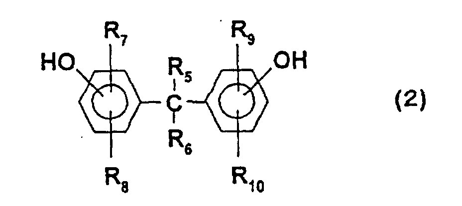
- the positive photosensitive resin composition contains a bisphenol compound represented by the following general formula (2) and a trisphenol compound represented by the following general formula (3) in a total amount of 1 to 30 parts by weight: wherein R 5 and R 6 are each a hydrogen atom or an alkyl group; R 7 , R 8 , R 9 and R 10 are each one atom or group selected from hydrogen atom, a halogen atom, hydroxyl group, an alkoxy group, a cycloalkyl group and an alkyl group, and wherein R 11 is hydrogen atom or an alkyl group; and R 12 , R 13 , R 14 , R 15 , R 16 and R 17 are each one atom or group selected from hydrogen atom, a halogen atom, hydroxyl group, an alkyl group, an alkoxy group and a cycloalkyl group.
- R 5 and R 6 are each a hydrogen atom or an alkyl group
- R 7 , R 8 , R 9 and R 10 are each one atom
- the proportions of the bisphenol compound and the trisphenol compound are 10:90 to 90:10.
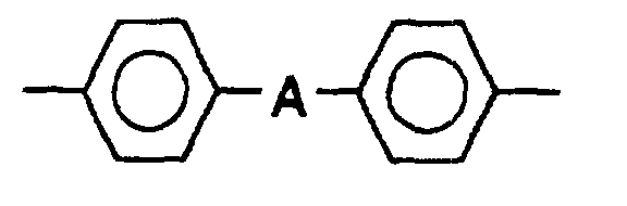
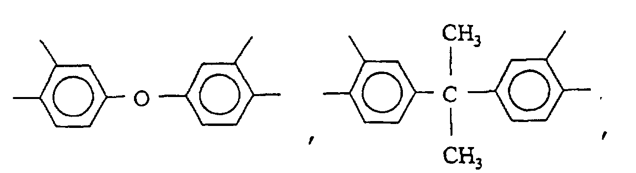
- the X of the polyamide is selected from the followings:
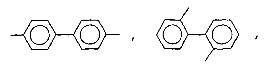
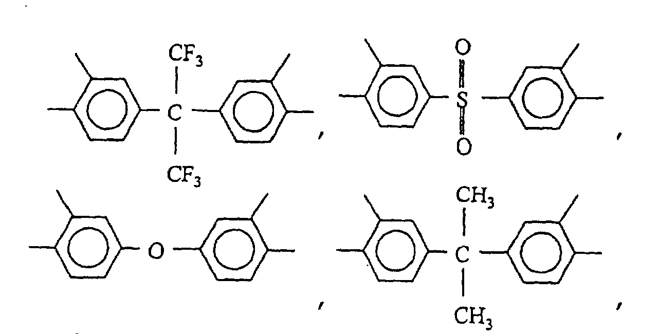
- the Y of the polyamide is selected from the followings: and wherein A is -CH 2 -, -C(CH 3 ) 2 -, -O-, -S-, -SO 2 -, -CO-, -NHCO- or -C(CF 3 ) 2 -.
- the positive photosensitive resin composition is cured at a temperature of 280 to 440°C.
- Figs. 1 to 4 have the followings meanings.
- the polyamide of the formula (1) is composed of a bisaminophenol having a structure of X, a dicarboxylic acid having a structure of Y and an acid anhydride having a structure of E.
- This polyamide when heated at about 280 to 440°C, gives rise to dehydration and ring closure and is converted into a heat-resistant resin called polybenzoxazole.
- the X of the polyamide (1) of the present invention is, for example, one of the followings: wherein A is -CH 2 -, -C(CH 3 ) 2 -, -O-, -S-, -SO 2 -, -CO-, -NHCO- or -C(CF 3 ) 2 -.
- A is -CH 2 -, -C(CH 3 ) 2 -, -O-, -S-, -SO 2 -, -CO-, -NHCO- or -C(CF 3 ) 2 -.
- the X is not restricted thereto.
- the Y of the formula (1) is, for example, one of the followings: and wherein A is -CH 2 -, -C(CH 3 ) 2 -, -O-, -S-, -SO 2 -, -CO-, -NHCO- or -C(CF 3 ) 2 -.
- A is -CH 2 -, -C(CH 3 ) 2 -, -O-, -S-, -SO 2 -, -CO-, -NHCO- or -C(CF 3 ) 2 -.
- the Y is not restricted thereto.
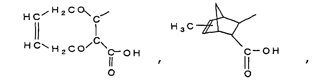
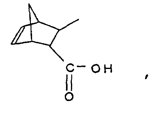
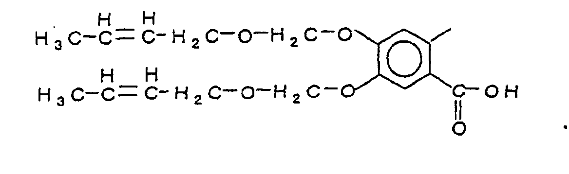
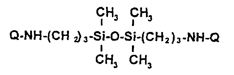
- the E of the formula (1) includes, for example, the followings: and However, the E is not restricted thereto.
- a dicarboxylic acid derivative having a Y structure is reacted with a bisaminophenol having an X structure, to synthesize a polyamide, after which the terminal amino groups of the polyamide are capped with an acid anhydride having at least one alkenyl or alkinyl group, represented by the E of the formula (1).
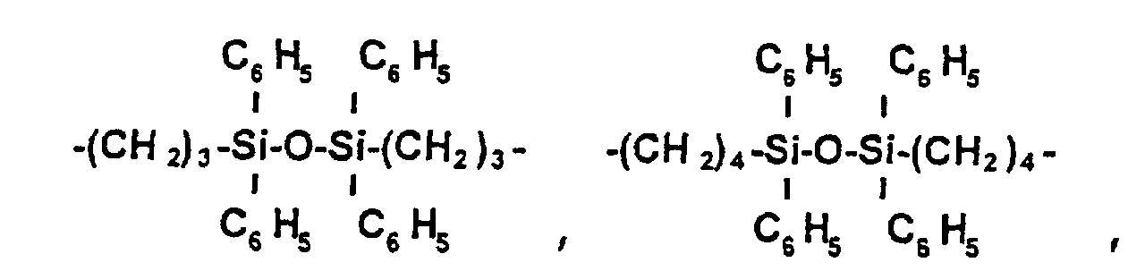
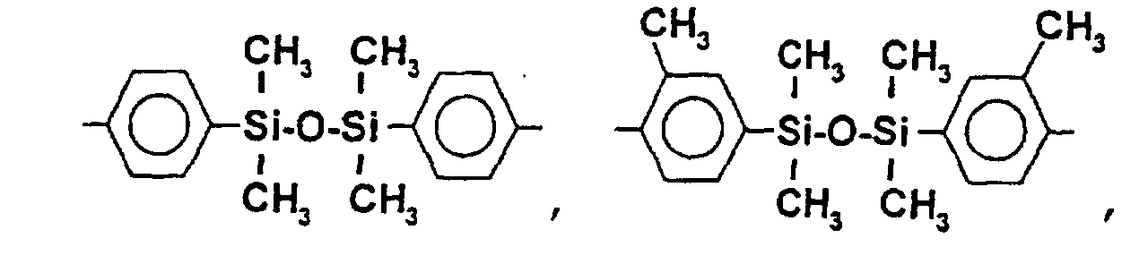
- the Z of the formula (1) is, for example, one of the followings: and However, the Z is not restricted thereto.
- the Z of the formula (1) is used, for example, when very high adhesivity to a substrate (e.g. silicon wafer) is required.
- the proportion b of the Z used is 40 mole % or less. When the proportion is more than 40 mole %, the resulting resin has very low solubility, resulting in scum generation and no pattern formation.
- each of the X, Y, E and Z used may be given by a single substance or a mixture of two or more kinds of substances.
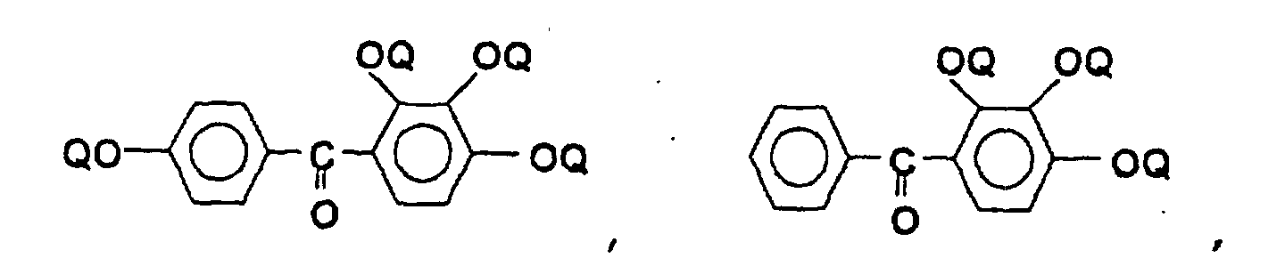
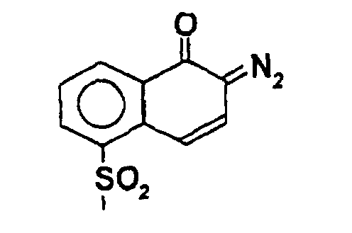
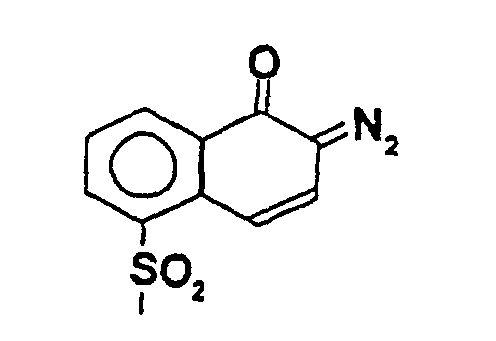
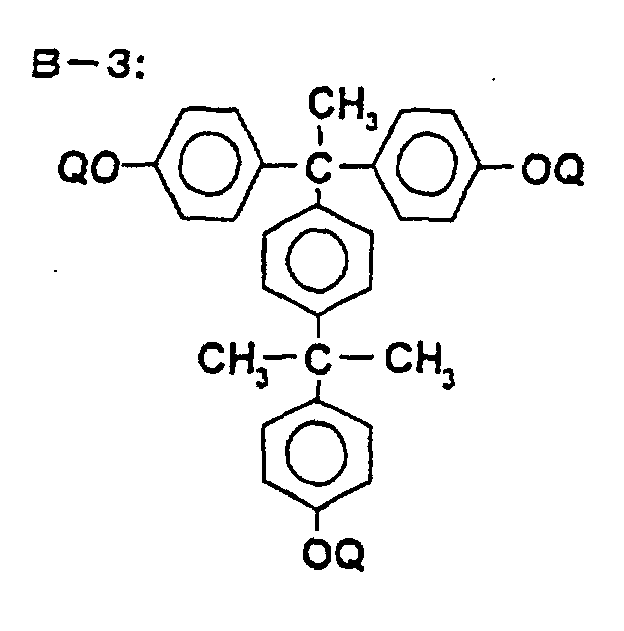
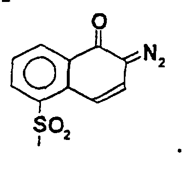
- the photosensitive diazoquinone compound used in the present invention is a reaction product between a compound having a 1,2-benzoquinone diazide or 1,2-naphthoquinone diazide structure and a phenol type compound which is a substrate.
- the composition of the present invention it is important to allow the composition to contain a photosensitive diazoquinone compound so that, in particular, a high sensitivity and a high residual film ratio can be obtained during the development of the composition.
- the development of a positive photosensitive resin is conducted by utilizing the difference in solubility between the exposed and non-exposed portions of the resin.
- the exposed portion is highly soluble and the non-exposed portion is highly insoluble so that the difference in solubility between the exposed and non-exposed portions becomes as large as possible.
- the difference in solubility between the exposed and non-exposed portions is largely dependent upon the structure of the phenol type compound which is a substrate.
- the photosensitive diazoquinone compound includes the following compounds but is not restricted thereto: and wherein each Q is selected from hydrogen atom, and, in each compound, at least one Q is
- the proportion of the photosensitive diazoquinone compound relative to the polyamide is 1 to 100 parts by weight relative to 100 parts by weight of the polyamide.
- the proportion is less than 1 part by weight, the resulting resin is inferior in pattern-formability.
- the proportion is more than 100 parts by weight, there occur a large decrease in sensitivity and a significant reduction in tensile elongation of the resulting film.
- the positive photosensitive resin composition of the present invention may contain, as necessary, a dihydropyridine derivative for higher photosensitivity.
- a dihydropyridine derivative for higher photosensitivity.
- the dihydropyridine derivative there can be mentioned, for example, 2,6-dimethyl-3,5-diacetyl-4-(2'-nitrophenyl)-1,4-dihydropyridine, 4-(2'-nitrophenyl)-2,6-dimethyl-3,5-dicarboethoxy-1,4-dihydropyridine and 4-(2',4'-dinitrophenyl)-2,6-dimethyl-3,5-dicarbomethoxy-1,4-dihydropyridine.
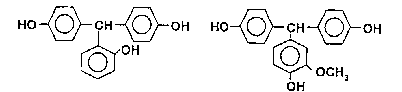
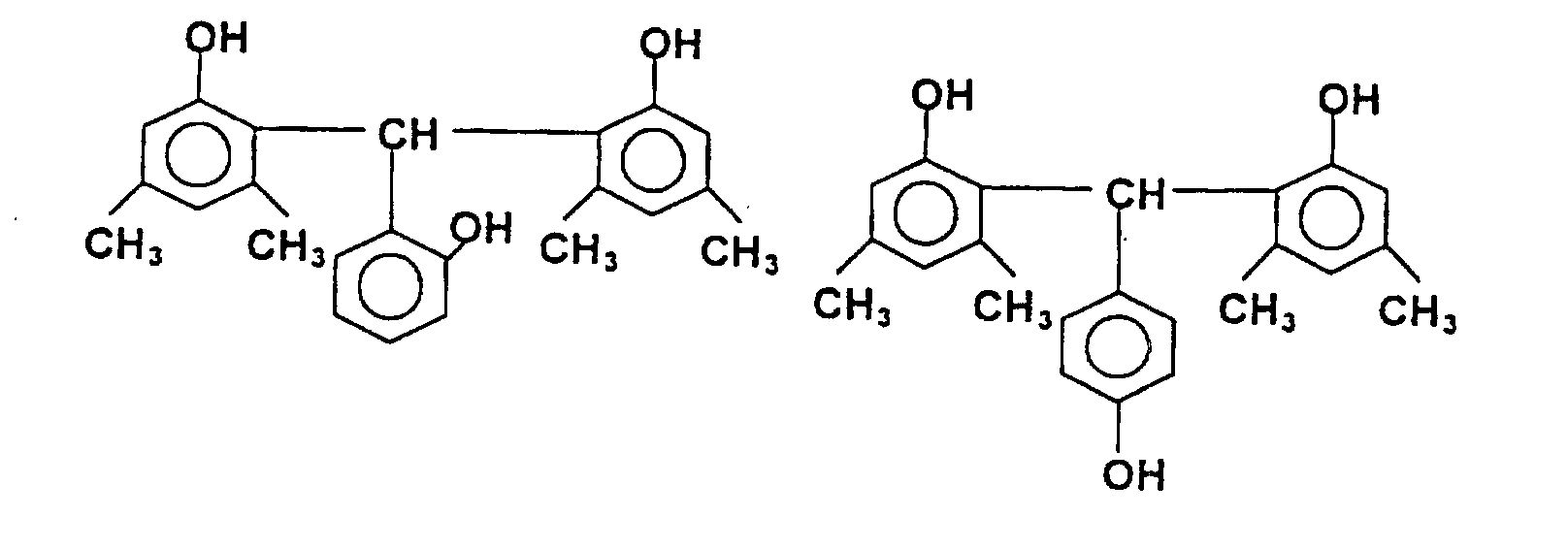
- the positive photosensitive resin composition of the present invention further contains a combination of a bisphenol compound represented by the general formula (2) and a trisphenol compound represented by the general formula (3).
- a positive photosensitive resin composition constituted by a polybenzoxazole precursor and a diazoquinone compound
- a positive photosensitive resin composition which has increased adhesivity to an encapsulating resin, shows a high sensitivity and gives a high residual film ratio, in development, and causes no deposition of phenol even when stored at a low temperature of -60 to -50°C and has excellent storability.
- Adhesivity to an encapsulating resin can be obtained to a certain extent even when only either of the phenol compounds represented by the general formulas (2) and (3) is added.
- an increase in addition amount tends to cause deposition of phenol upon storage of the resin composition at a low temperature of -60 to -50°C.
- an increase in addition amount causes a significant reduction in residual film ratio.
- the bisphenol compound represented by the general formula (2) and the trisphenol compound represented by the general formula (3) are used in combination, the problems possessed by the individual compounds are alleviated, and an even higher photosensitivity and excellent adhesivity to an encapsulating resin can be obtained.
- the addition amount of the phenol compounds are 1 to 30 parts in the total amount of the bisphenol compound represented by the general formula (2) and the trisphenol compound represented by the general formula (3), relative to 100 parts by weight of the polyamide represented by the general formula (1).
- the addition amount of the two phenol compounds is more than 30 parts by weight, a deposit is generated in the low-temperature (-60 to -50°C) storage of the resin composition as mentioned before and a significant reduction in residual film ratio appears during development.
- the addition amount is less than 1 part by weight, there occur not only a reduction in adhesivity to an encapsulating resin but also a decrease in sensitivity during development.
- the proportions of the bisphenol compound and the trisphenol compound are 10:90 to 90:10. When the proportion of the bisphenol compound is less than 10, a reduction in residual film ratio appears. When the proportion is more than 90, deposition takes place.
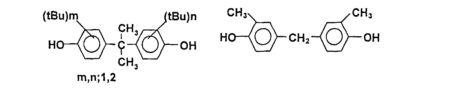
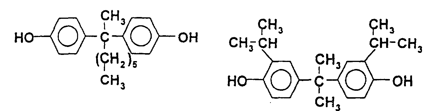
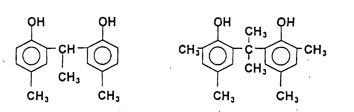
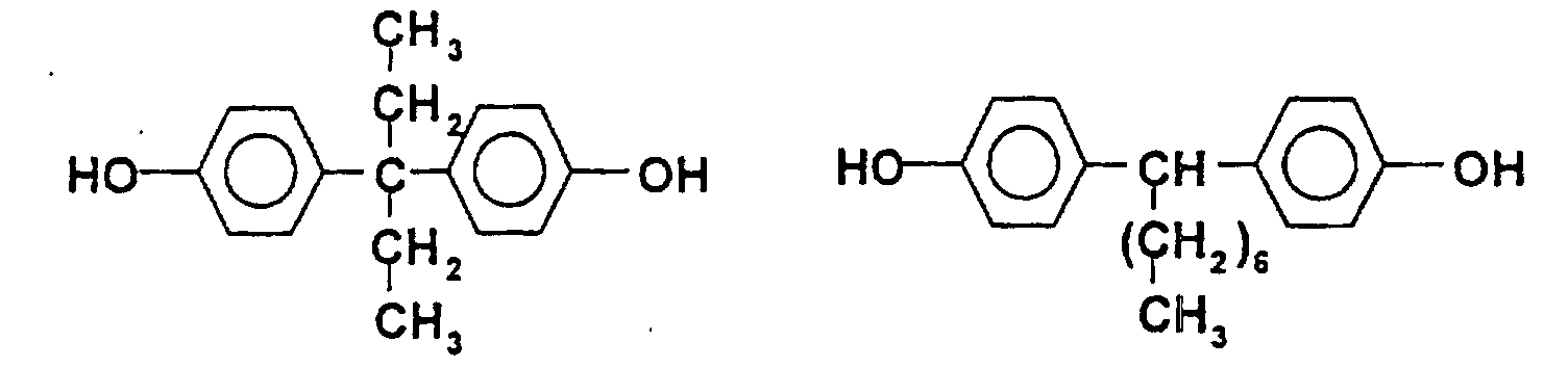
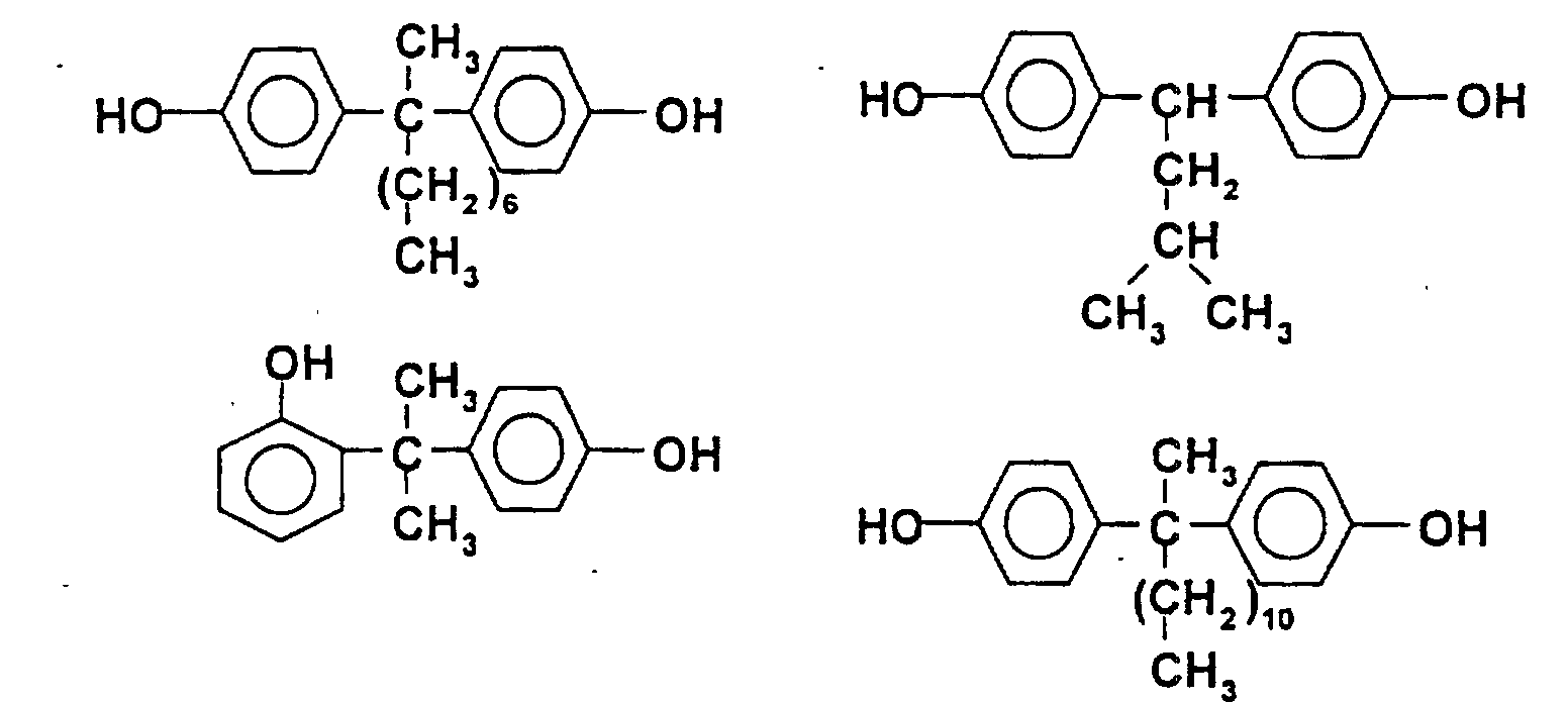
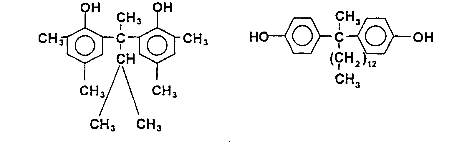
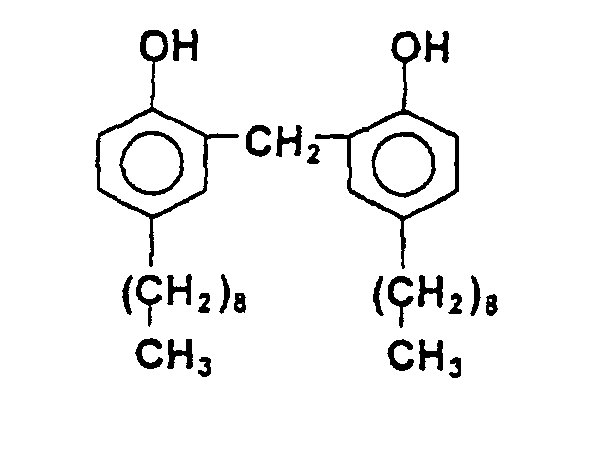
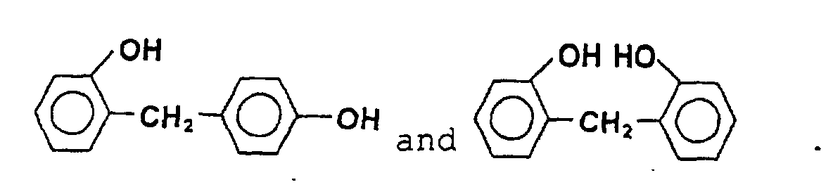
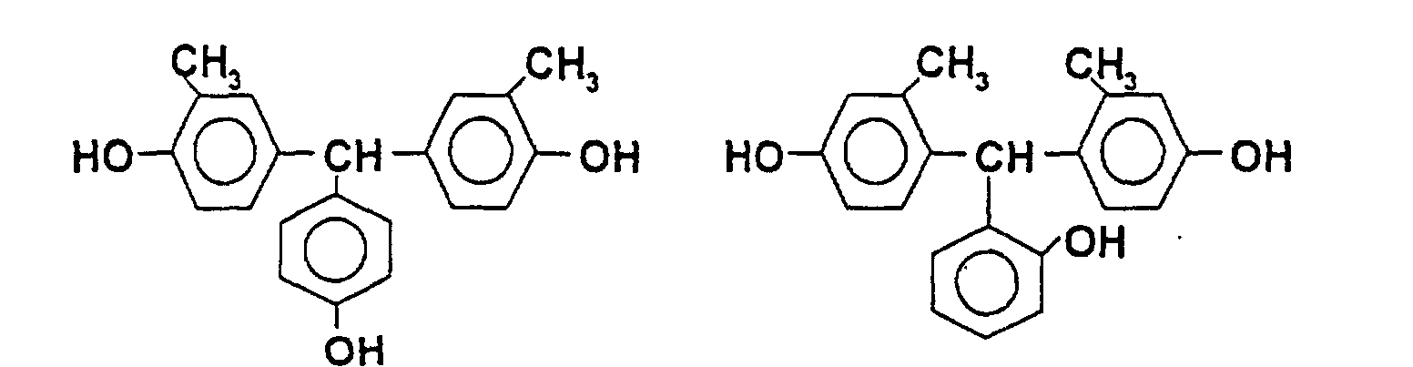
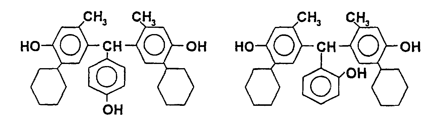
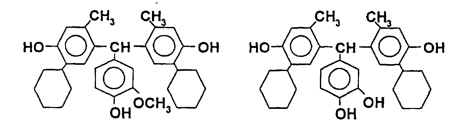
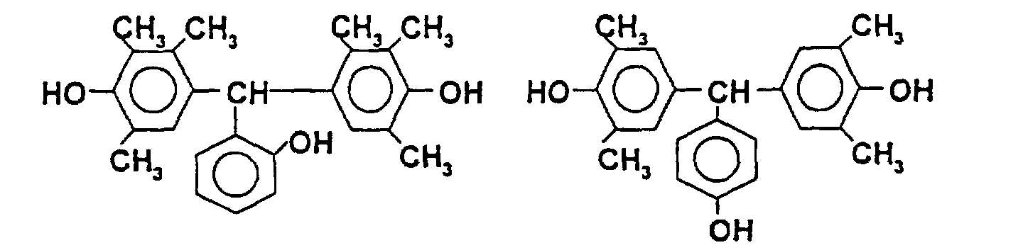
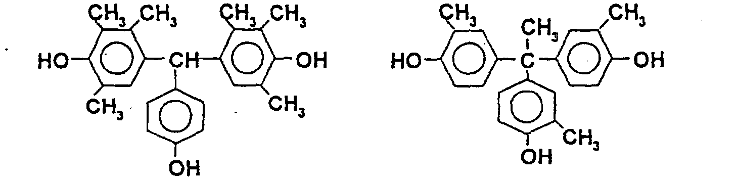
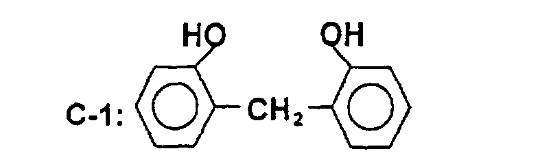
- the bisphenol compound represented by the general formula (2) for example, the following compounds can be mentioned.
- the bisphenol compound (2) is not restricted thereto.
- particularly preferred are:
- the positive photosensitive resin composition of the present invention can contain, as necessary, additives such as leveling agent, silane coupling agent and the like.
- these components are dissolved in a solvent and used in a varnish state.
- the solvent there can be mentioned N-methyl-2-pyrrolidone, ⁇ -butyrolactone, N,N-dimethylacetamide, dimethyl sulfoxide, diethylene glycol dimethyl ether, diethylene glycol diethyl ether, diethylene glycol dibutyl ether, propylene glycol monomethyl ether, dipropylene glycol monomethyl ether, propylene glycol monomethyl ether acetate, methyl lactate, ethyl lactate, butyl lactate, methyl-1,3-butylene glycol acetate, 1,3-butylene glycol-3-monomethyl ether, methyl pyruvate, ethyl pyruvate, methyl-3-methoxypropionate, etc.
- These solvents may be used singly or in admixture.
- the composition is coated on an appropriate substrate, for example, a silicon wafer, a ceramic substrate or an aluminum substrate.
- the amount of the composition coated is, in production of a semiconductor device, such that the final film thickness after curing becomes 0.1 to 20 ⁇ m.
- the film thickness is less than 0.1 ⁇ m, the film is unable to sufficiently exhibit the function as a protective surface film for a semiconductor chip.
- the film thickness is more than 20 ⁇ m, it is difficult to obtain a fine pattern and, moreover, a long time is taken for processing, resulting in reduced throughput.
- the method for coating there are spin coating using a spinner, spray coating using a spray coater, immersion, printing, roll coating, etc.
- prebaking is conducted at 60 to 130°C to dry the coating film, after which an actinic ray is applied in a desired pattern.
- an actinic ray there can be used an X-ray, an electron beam, an ultraviolet light, a visible light, etc.; however, an actinic ray having a wavelength of 200 to 500 nm is preferred.
- the actinic ray-applied portion is dissolved and removed with a developing solution to obtain a relief pattern.
- an aqueous solution of an alkali e.g., an inorganic alkali such as sodium hydroxide, potassium hydroxide, sodium carbonate, sodium silicate, sodium metasilicate, ammonia water or the like; a primary amine such as ethylamine, n-propylamine or the like; a secondary amine such as diethylamine, di-n-propylamine or the like; a tertiary amine such as triethylamine, methyldiethylamine or the like; an alcohol amine such as dimethylethanolamine, triethanolamine or the like; or a quaternary ammonium salt such as tetramethylammonium hydroxide, tetraethylammonium hydroxide or the like, or an aqueous solution obtained by adding, to the above aqueous solution, an appropriate amount of a water-soluble organic solvent, e.g., an alcohol such as methanol
- the relief pattern formed by development is rinsed.
- distilled water is used as the rinsing liquid.
- a heat treatment is applied at 280 to 440°C to form an oxazole ring to obtain a final pattern of high heat resistance.
- the heat treatment is conducted preferably at 350 to 440°C because, in particular, the bump-forming step conducted later includes exposure to a chemical such as a flux and a high-temperature treatment.
- a chemical such as a flux and a high-temperature treatment.
- Fig. 1 is an enlarged sectional view of the pad portion of a semiconductor device having a bump, of the present invention.
- an Al pad 2 for input and output is formed on a silicon wafer 1; thereon is formed a passivation film 3; and a via hole is formed in the passivation film 3.
- a polybenzoxazole resin film (a buffer coat film) 4 is formed thereon; further, a metal (e.g.
- film 5 is formed so as to contact with the Al pad 2; the metal film 5 is removed by etching, in the vicinity of a solder bump 12 to secure insulation between pads.
- a barrier metal 8 and a solder bump 12 are formed for the insulated pad.
- each Q is hydrogen atom or and 70% of the total Qs is
- the above-obtained positive photosensitive resin composition was coated on a wafer using a spin coater, followed by drying on a hot plate at 120°C for 4 minutes to obtain a coating film having a thickness of about 5 ⁇ m.
- the resulting material was immersed in a 1.40% aqueous tetramethylammonium hydroxide solution to dissolve and remove the light-exposed portion, and rinsed with pure water for 30 seconds.
- the residual film ratio [(film thickness after development)/(film thickness before development)]x100 was very high at 93.1%.
- a wiring metal film was formed by plating.
- the positive photosensitive resin composition was coated and a pattern (an insulating film) 7 was formed via photolithography.
- a barrier metal 8 and a solder 10 were deposited in this order, by plating.
- a flux 11 was coated and the solder 10 was melted by heating.
- the flux 11 was removed by washing, to form a solder bump 12 as shown in Fig. 4b, and dicing was conducted along a scribing line to obtain individual chips.
- each Q is hydrogen atom or and 70% of the total Qs is
- each Q is hydrogen atom or and 60% of the total Qs is
- a flip chip similar to that of Example 1 was produced by using a photo-insensitive polyimide resin, CRC-6061 (a product of Sumitomo Bakelite Company Limited). Coating was made, by using a spin coater, on a wafer wherein a via hole had been formed in a passivation film using a resist. Then, drying was conducted on a hot plate at 140°C for 4 minutes to form a coating film having a thickness of about 5 ⁇ m. Thereon was coated a positive resist, OFPR-800 (a product of Tokyo Ohka Kogyo Co., Ltd.) by using a spin coater, followed by drying on a hot plate at 100°C for 2 minutes to obtain a coating film having a thickness of about 2 ⁇ m.
- OFPR-800 a product of Tokyo Ohka Kogyo Co., Ltd.
- the resulting material was subjected to curing in a clean oven under nitrogen atmosphere at 150°C for 30 minutes and at 400°C for 30 minutes.
- the water absorption of the cured film was 2.0%.
- the photo-insensitive polyimide gives inferior precision of processing, making it impossible to use the buffer coat layer as a mask for reactive ion etching (RIE); therefore, it was necessary to form a via hole in a passivation film by using a resist.
- the cured film has a high water absorption of 2.0% and is inferior in reliability.
- a passivation layer is etched by using a photosensitive buffer coat resin (a polybenzoxazole resin precursor) as a mask; therefore, the present invention, as compared with conventional techniques, enables a significant reduction in operational steps. Further, the polybenzoxazole resin of the present invention is low in water absorption and superior in adhesivity to an encapsulating resin; therefore, can provide an inexpensive and highly reliable semiconductor device.
- a photosensitive buffer coat resin a polybenzoxazole resin precursor
- the semiconductor device having a positive photosensitive resin composition and provided with a bump electrode, according to the present invention can be used for electric or electronic products such as computers including personal computers, televisions, video decks and the like.
Landscapes
- Chemical & Material Sciences (AREA)
- Physics & Mathematics (AREA)
- Spectroscopy & Molecular Physics (AREA)
- Chemical Kinetics & Catalysis (AREA)
- Organic Chemistry (AREA)
- General Physics & Mathematics (AREA)
- Polymers & Plastics (AREA)
- Engineering & Computer Science (AREA)
- Materials Engineering (AREA)
- Wood Science & Technology (AREA)
- Life Sciences & Earth Sciences (AREA)
- Health & Medical Sciences (AREA)
- Medicinal Chemistry (AREA)
- Materials For Photolithography (AREA)
- Formation Of Insulating Films (AREA)
- Application Of Or Painting With Fluid Materials (AREA)
- Structures Or Materials For Encapsulating Or Coating Semiconductor Devices Or Solid State Devices (AREA)
- Polyamides (AREA)
Abstract
Description


1: Silicon wafer, 2: Al pad, 3: passivation film,
4: buffer coat film; 5: metal (e.g. Cr or Ti) film,
6: wiring (e.g. Al or Cu), 7: insulating film,
8: barrier metal, 9: resist, 10: solder
11: flux, 12: solder bump




































Claims (6)
- A semiconductor device comprising:wherein X is a tetravalent aromatic group; Y is a bivalent aromatic group; Z is(a) a polybenzoxazole resin film for chip protection, obtained by coating, on a circuit-formed chip, a positive photosensitive resin composition comprising 100 parts by weight of a polyamide represented by the following general formula (1) and 1 to 100 parts by weight of a photosensitive diazoquinone compound, and subjecting the coated composition to patterning and curing, and(b) a bump electrode:
 (R1 and R2 are each a bivalent organic group, and R3 and R4 are each a monovalent organic group); E is a carboxyl aliphatic, alicyclic or aromatic group having at least one alkenyl or alkinyl group; and a and b are each a molar fraction, a + b = 100 mole %, a = 60.0 to 100.0 mole % and b = 0 to 40.0 mole %; and n = 2 to 500.
- A semiconductor device according to Claim 1, wherein the positive photosensitive resin composition contains a bisphenol compound represented by the following general formula (2) and a trisphenol compound represented by the following general formula (3) in a total amount of 1 to 30 parts by weight:wherein R5 and R6 are each hydrogen atom or an alkyl group; R7, R8, R9 and R10 are each one atom or group selected from hydrogen atom, a halogen atom, hydroxyl group, an alkoxy group, a cycloalkyl group and an alkyl group, and
 wherein R11 is hydrogen atom or an alkyl group; and R12, R13, R14, R15, R16 and R17 are each one atom or group selected from hydrogen atom, a halogen atom, hydroxyl group, an alkyl group, an alkoxy group and a cycloalkyl group.
- A semiconductor device according to Claim 2, wherein the proportions of the bisphenol compound and the trisphenol compound are 10:90 to 90:10.
- A semiconductor device according to Claim 1 or 2, wherein the X of the polyamide is selected from the followings:and

- A semiconductor device according to Claim 1 or 2, wherein the Y of the polyamide is selected from the followings:
 and
and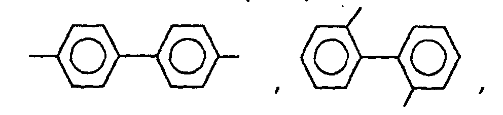 wherein A is -CH2-, -C(CH3)2-, -O-, -S-, -SO2-, -CO-, -NHCO- or -C(CF3)2-.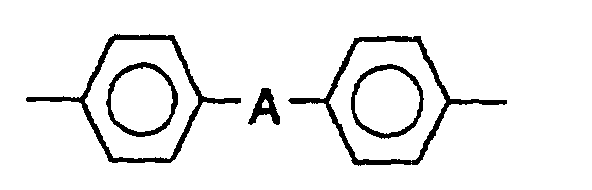
- A semiconductor device according to Claim 1, wherein the positive photosensitive resin composition is cured at a temperature of 280 to 440°C.
Applications Claiming Priority (5)
| Application Number | Priority Date | Filing Date | Title |
|---|---|---|---|
| JP5142299 | 1999-02-26 | ||
| JP5142299 | 1999-02-26 | ||
| JP2000039079A JP3667184B2 (en) | 1999-02-26 | 2000-02-17 | Semiconductor device |
| JP2000039079 | 2000-02-17 | ||
| PCT/JP2000/001028 WO2000052757A1 (en) | 1999-02-26 | 2000-02-23 | Semiconductor device |
Publications (3)
| Publication Number | Publication Date |
|---|---|
| EP1195811A1 true EP1195811A1 (en) | 2002-04-10 |
| EP1195811A4 EP1195811A4 (en) | 2002-05-15 |
| EP1195811B1 EP1195811B1 (en) | 2003-10-15 |
Family
ID=26391954
Family Applications (1)
| Application Number | Title | Priority Date | Filing Date |
|---|---|---|---|
| EP00905287A Expired - Lifetime EP1195811B1 (en) | 1999-02-26 | 2000-02-23 | Semiconductor device |
Country Status (8)
| Country | Link |
|---|---|
| US (1) | US6576381B1 (en) |
| EP (1) | EP1195811B1 (en) |
| JP (1) | JP3667184B2 (en) |
| KR (1) | KR100695636B1 (en) |
| CN (1) | CN1198334C (en) |
| DE (1) | DE60005959T2 (en) |
| TW (1) | TW500978B (en) |
| WO (1) | WO2000052757A1 (en) |
Cited By (3)
| Publication number | Priority date | Publication date | Assignee | Title |
|---|---|---|---|---|
| WO2006132962A2 (en) | 2005-06-03 | 2006-12-14 | Fujifilm Electronic Materials U.S.A. Inc. | Novel photosensitive resin compositions |
| US7238455B2 (en) | 2003-06-23 | 2007-07-03 | Sumitomo Bakelite Company, Ltd. | Positive-working photosensitive resin composition, method for producing pattern-formed resin film, semiconductor device, display device, and method for producing the semiconductor device and the display device |
| EP1815515A4 (en) * | 2004-10-29 | 2009-03-11 | Flipchip Internat L L C | SEMICONDUCTOR DEVICE HOUSING COMPRISING A POLYMERIC LAYER SURMOUNTED OVER A BOSSAGE |
Families Citing this family (17)
| Publication number | Priority date | Publication date | Assignee | Title |
|---|---|---|---|---|
| JP2002341521A (en) * | 2001-05-17 | 2002-11-27 | Sumitomo Chem Co Ltd | Radiation-sensitive resin composition |
| JP2003045877A (en) * | 2001-08-01 | 2003-02-14 | Sharp Corp | Semiconductor device and method of manufacturing the same |
| CN1287435C (en) * | 2002-06-27 | 2006-11-29 | 松下电器产业株式会社 | Semiconductor device and manufacturing method thereof |
| US6887643B2 (en) * | 2002-08-05 | 2005-05-03 | Toray Industries, Inc. | Photosensitive resin precursor composition |
| JP4327657B2 (en) * | 2004-05-20 | 2009-09-09 | Necエレクトロニクス株式会社 | Semiconductor device |
| JP2008546204A (en) * | 2005-06-03 | 2008-12-18 | フジフィルム・エレクトロニック・マテリアルズ・ユーエスエイ・インコーポレイテッド | Pretreatment composition |
| SG175668A1 (en) * | 2006-10-24 | 2011-11-28 | Sumitomo Bakelite Co | Bis(aminophenol) derivative, process for producing the same, polyamide resin, positive photosensitive resin compositions, protective film, interlayer dielectric, semiconductor device, and display element |
| US9524945B2 (en) | 2010-05-18 | 2016-12-20 | Taiwan Semiconductor Manufacturing Company, Ltd. | Cu pillar bump with L-shaped non-metal sidewall protection structure |
| JP5410918B2 (en) * | 2008-10-20 | 2014-02-05 | チェイル インダストリーズ インコーポレイテッド | Positive photosensitive resin composition |
| WO2010089814A1 (en) * | 2009-02-04 | 2010-08-12 | パナソニック株式会社 | Semiconductor substrate structure and semiconductor device |
| US8377816B2 (en) * | 2009-07-30 | 2013-02-19 | Taiwan Semiconductor Manufacturing Company, Ltd. | Method of forming electrical connections |
| US8841766B2 (en) | 2009-07-30 | 2014-09-23 | Taiwan Semiconductor Manufacturing Company, Ltd. | Cu pillar bump with non-metal sidewall protection structure |
| US8324738B2 (en) * | 2009-09-01 | 2012-12-04 | Taiwan Semiconductor Manufacturing Company, Ltd. | Self-aligned protection layer for copper post structure |
| US8659155B2 (en) * | 2009-11-05 | 2014-02-25 | Taiwan Semiconductor Manufacturing Company, Ltd. | Mechanisms for forming copper pillar bumps |
| US8610270B2 (en) * | 2010-02-09 | 2013-12-17 | Taiwan Semiconductor Manufacturing Company, Ltd. | Semiconductor device and semiconductor assembly with lead-free solder |
| US8441124B2 (en) | 2010-04-29 | 2013-05-14 | Taiwan Semiconductor Manufacturing Company, Ltd. | Cu pillar bump with non-metal sidewall protection structure |
| US9018758B2 (en) | 2010-06-02 | 2015-04-28 | Taiwan Semiconductor Manufacturing Company, Ltd. | Cu pillar bump with non-metal sidewall spacer and metal top cap |
Family Cites Families (9)
| Publication number | Priority date | Publication date | Assignee | Title |
|---|---|---|---|---|
| US5194934A (en) * | 1988-07-27 | 1993-03-16 | Semiconductor Energy Laboratory Co., Ltd. | Mounting structure for a semiconductor chip having a buffer layer |
| DE59208963D1 (en) | 1991-05-07 | 1997-11-20 | Siemens Ag | Highly heat-resistant positive resists and process for the production of highly heat-resistant relief structures |
| US5162257A (en) * | 1991-09-13 | 1992-11-10 | Mcnc | Solder bump fabrication method |
| KR0181615B1 (en) * | 1995-01-30 | 1999-04-15 | 모리시다 요이치 | Semiconductor unit package, semiconductor unit packaging method, and encapsulant for use in semiconductor unit packaging |
| DE69617928T2 (en) * | 1995-03-20 | 2002-07-18 | Unitive International Ltd., Curacao | SOLDER BUMPER MANUFACTURING METHOD AND STRUCTURES WITH A TITANIUM BARRIER |
| TW502135B (en) * | 1996-05-13 | 2002-09-11 | Sumitomo Bakelite Co | Positive type photosensitive resin composition and process for preparing polybenzoxazole resin film by using the same |
| US6222272B1 (en) * | 1996-08-06 | 2001-04-24 | Nitto Denko Corporation | Film carrier and semiconductor device using same |
| JPH1135915A (en) * | 1997-07-15 | 1999-02-09 | Toray Ind Inc | Resin-sealed semiconductor device |
| JPH11312675A (en) * | 1998-04-27 | 1999-11-09 | Sumitomo Bakelite Co Ltd | Semiconductor device and manufacture thereof |
-
2000
- 2000-02-17 JP JP2000039079A patent/JP3667184B2/en not_active Expired - Fee Related
- 2000-02-23 US US09/913,156 patent/US6576381B1/en not_active Expired - Lifetime
- 2000-02-23 CN CNB008042306A patent/CN1198334C/en not_active Expired - Fee Related
- 2000-02-23 WO PCT/JP2000/001028 patent/WO2000052757A1/en not_active Ceased
- 2000-02-23 KR KR1020017010908A patent/KR100695636B1/en not_active Expired - Lifetime
- 2000-02-23 DE DE60005959T patent/DE60005959T2/en not_active Expired - Lifetime
- 2000-02-23 EP EP00905287A patent/EP1195811B1/en not_active Expired - Lifetime
- 2000-02-24 TW TW089103281A patent/TW500978B/en not_active IP Right Cessation
Cited By (7)
| Publication number | Priority date | Publication date | Assignee | Title |
|---|---|---|---|---|
| US7238455B2 (en) | 2003-06-23 | 2007-07-03 | Sumitomo Bakelite Company, Ltd. | Positive-working photosensitive resin composition, method for producing pattern-formed resin film, semiconductor device, display device, and method for producing the semiconductor device and the display device |
| EP1491952A3 (en) * | 2003-06-23 | 2007-07-25 | Sumitomo Bakelite Co., Ltd. | Positive-working photosensitive resin composition, method for producing pattern-formed resin film, semiconductor device, display device, and method for producing the semiconductor device and the display device |
| US7361445B2 (en) | 2003-06-23 | 2008-04-22 | Sumitomo Bakelite Company | Positive-working photosensitive resin composition, method for producing pattern-formed resin film, semiconductor device, display device, and method for producing the semiconductor device and the display device |
| EP2381308A3 (en) * | 2003-06-23 | 2012-03-21 | Sumitomo Bakelite Co., Ltd. | Positive-working photosensitive resin composition, method for producing pattern-formed resin film, semiconductor device, display device, and method for producing the semiconductor device and the display device |
| EP1815515A4 (en) * | 2004-10-29 | 2009-03-11 | Flipchip Internat L L C | SEMICONDUCTOR DEVICE HOUSING COMPRISING A POLYMERIC LAYER SURMOUNTED OVER A BOSSAGE |
| WO2006132962A2 (en) | 2005-06-03 | 2006-12-14 | Fujifilm Electronic Materials U.S.A. Inc. | Novel photosensitive resin compositions |
| EP1886187A4 (en) * | 2005-06-03 | 2010-10-06 | Fujifilm Electronic Materials | Novel photosensitive resin compositions |
Also Published As
| Publication number | Publication date |
|---|---|
| KR20010111495A (en) | 2001-12-19 |
| WO2000052757A1 (en) | 2000-09-08 |
| TW500978B (en) | 2002-09-01 |
| KR100695636B1 (en) | 2007-03-15 |
| CN1198334C (en) | 2005-04-20 |
| DE60005959D1 (en) | 2003-11-20 |
| JP3667184B2 (en) | 2005-07-06 |
| EP1195811A4 (en) | 2002-05-15 |
| EP1195811B1 (en) | 2003-10-15 |
| CN1341279A (en) | 2002-03-20 |
| DE60005959T2 (en) | 2004-08-12 |
| US6576381B1 (en) | 2003-06-10 |
| JP2000310858A (en) | 2000-11-07 |
Similar Documents
| Publication | Publication Date | Title |
|---|---|---|
| EP1195811B1 (en) | Semiconductor device | |
| EP1331517B1 (en) | Positive photosensitive resin composition, process for its preparation, and semiconductor devices | |
| JP5339087B2 (en) | Positive photosensitive resin composition, cured film, protective film, insulating film, and semiconductor device | |
| TW201346448A (en) | Positive type photosensitive resin composition, semiconductor device and display device using the same | |
| JPH09302221A (en) | Positive photosensitive resin composition | |
| JP3919147B2 (en) | Positive photosensitive resin composition and semiconductor device using the same | |
| JP3449925B2 (en) | Positive photosensitive resin composition | |
| JP4661245B2 (en) | Positive photosensitive resin composition, semiconductor device and display element using the positive photosensitive resin composition, and manufacturing method of semiconductor device and display element | |
| JP4254177B2 (en) | Positive photosensitive resin composition and semiconductor device | |
| JP2006010781A (en) | Positive photosensitive resin composition, semiconductor device, display element, and method for manufacturing semiconductor device and display element | |
| JP3422691B2 (en) | Positive photosensitive resin composition | |
| JPH11312675A (en) | Semiconductor device and manufacture thereof | |
| JP3992351B2 (en) | Positive photosensitive resin composition and semiconductor device using the same | |
| JP3449926B2 (en) | Positive photosensitive resin composition | |
| JP4250935B2 (en) | Positive photosensitive resin composition and semiconductor device | |
| JP3886334B2 (en) | Positive photosensitive resin composition and semiconductor device | |
| JP3313331B2 (en) | Resin-sealed semiconductor device | |
| JP3449933B2 (en) | Positive photosensitive resin composition and semiconductor device using the same | |
| JPH09321038A (en) | Semiconductor device | |
| JP4345441B2 (en) | Positive photosensitive resin composition and semiconductor device | |
| JP4332958B2 (en) | Method for processing positive photosensitive resin composition and semiconductor device | |
| JP4166058B2 (en) | Positive photosensitive resin composition and semiconductor device | |
| JP2001100415A (en) | Positive type photosensitive resin composition and semiconductor device using same | |
| JP2000131844A (en) | Positive photosensitive resin composition and semiconductor device made by using the same | |
| JP2001154356A (en) | Positive type photosensitive resin composition and semiconductor device |
Legal Events
| Date | Code | Title | Description |
|---|---|---|---|
| PUAI | Public reference made under article 153(3) epc to a published international application that has entered the european phase |
Free format text: ORIGINAL CODE: 0009012 |
|
| 17P | Request for examination filed |
Effective date: 20010824 |
|
| AK | Designated contracting states |
Kind code of ref document: A1 Designated state(s): AT BE CH CY DE DK ES FI FR GB GR IE IT LI LU MC NL PT SE |
|
| A4 | Supplementary search report drawn up and despatched |
Effective date: 20020404 |
|
| AK | Designated contracting states |
Kind code of ref document: A4 Designated state(s): AT BE CH CY DE DK ES FI FR GB GR IE IT LI LU MC NL PT SE |
|
| RIC1 | Information provided on ipc code assigned before grant |
Free format text: 7C 08G 73/22 A, 7H 01L 23/29 B, 7H 01L 21/312 B, 7H 01L 21/027 B, 7G 03F 7/022 B, 7G 03F 7/038 B, 7G 03F 7/075 B, 7C 08G 69/42 B, 7H 01L 21/60 B |
|
| 17Q | First examination report despatched |
Effective date: 20020813 |
|
| GRAH | Despatch of communication of intention to grant a patent |
Free format text: ORIGINAL CODE: EPIDOS IGRA |
|
| GRAS | Grant fee paid |
Free format text: ORIGINAL CODE: EPIDOSNIGR3 |
|
| GRAA | (expected) grant |
Free format text: ORIGINAL CODE: 0009210 |
|
| AK | Designated contracting states |
Kind code of ref document: B1 Designated state(s): DE FR GB NL |
|
| REG | Reference to a national code |
Ref country code: GB Ref legal event code: FG4D |
|
| REG | Reference to a national code |
Ref country code: IE Ref legal event code: FG4D |
|
| REF | Corresponds to: |
Ref document number: 60005959 Country of ref document: DE Date of ref document: 20031120 Kind code of ref document: P |
|
| ET | Fr: translation filed | ||
| PLBE | No opposition filed within time limit |
Free format text: ORIGINAL CODE: 0009261 |
|
| STAA | Information on the status of an ep patent application or granted ep patent |
Free format text: STATUS: NO OPPOSITION FILED WITHIN TIME LIMIT |
|
| 26N | No opposition filed |
Effective date: 20040716 |
|
| REG | Reference to a national code |
Ref country code: IE Ref legal event code: MM4A |
|
| REG | Reference to a national code |
Ref country code: FR Ref legal event code: PLFP Year of fee payment: 16 |
|
| PGFP | Annual fee paid to national office [announced via postgrant information from national office to epo] |
Ref country code: NL Payment date: 20150110 Year of fee payment: 16 |
|
| PGFP | Annual fee paid to national office [announced via postgrant information from national office to epo] |
Ref country code: DE Payment date: 20150218 Year of fee payment: 16 |
|
| PGFP | Annual fee paid to national office [announced via postgrant information from national office to epo] |
Ref country code: GB Payment date: 20150218 Year of fee payment: 16 Ref country code: FR Payment date: 20150210 Year of fee payment: 16 |
|
| REG | Reference to a national code |
Ref country code: DE Ref legal event code: R119 Ref document number: 60005959 Country of ref document: DE |
|
| GBPC | Gb: european patent ceased through non-payment of renewal fee |
Effective date: 20160223 |
|
| REG | Reference to a national code |
Ref country code: NL Ref legal event code: MM Effective date: 20160301 |
|
| REG | Reference to a national code |
Ref country code: FR Ref legal event code: ST Effective date: 20161028 |
|
| PG25 | Lapsed in a contracting state [announced via postgrant information from national office to epo] |
Ref country code: GB Free format text: LAPSE BECAUSE OF NON-PAYMENT OF DUE FEES Effective date: 20160223 Ref country code: FR Free format text: LAPSE BECAUSE OF NON-PAYMENT OF DUE FEES Effective date: 20160229 Ref country code: DE Free format text: LAPSE BECAUSE OF NON-PAYMENT OF DUE FEES Effective date: 20160901 Ref country code: NL Free format text: LAPSE BECAUSE OF NON-PAYMENT OF DUE FEES Effective date: 20160301 |