EP1195809A2 - Process for producing semiconductor device - Google Patents
Process for producing semiconductor device Download PDFInfo
- Publication number
- EP1195809A2 EP1195809A2 EP01307357A EP01307357A EP1195809A2 EP 1195809 A2 EP1195809 A2 EP 1195809A2 EP 01307357 A EP01307357 A EP 01307357A EP 01307357 A EP01307357 A EP 01307357A EP 1195809 A2 EP1195809 A2 EP 1195809A2
- Authority
- EP
- European Patent Office
- Prior art keywords
- wafer
- adhesive layer
- sheet
- pressure sensitive
- chips
- Prior art date
- Legal status (The legal status is an assumption and is not a legal conclusion. Google has not performed a legal analysis and makes no representation as to the accuracy of the status listed.)
- Granted
Links
Images


Classifications
-
- H—ELECTRICITY
- H10—SEMICONDUCTOR DEVICES; ELECTRIC SOLID-STATE DEVICES NOT OTHERWISE PROVIDED FOR
- H10P—GENERIC PROCESSES OR APPARATUS FOR THE MANUFACTURE OR TREATMENT OF DEVICES COVERED BY CLASS H10
- H10P72/00—Handling or holding of wafers, substrates or devices during manufacture or treatment thereof
- H10P72/70—Handling or holding of wafers, substrates or devices during manufacture or treatment thereof for supporting or gripping
- H10P72/74—Handling or holding of wafers, substrates or devices during manufacture or treatment thereof for supporting or gripping using temporarily an auxiliary support
- H10P72/7402—Wafer tapes, e.g. grinding or dicing support tapes
-
- H—ELECTRICITY
- H10—SEMICONDUCTOR DEVICES; ELECTRIC SOLID-STATE DEVICES NOT OTHERWISE PROVIDED FOR
- H10P—GENERIC PROCESSES OR APPARATUS FOR THE MANUFACTURE OR TREATMENT OF DEVICES COVERED BY CLASS H10
- H10P54/00—Cutting or separating of wafers, substrates or parts of devices
-
- H—ELECTRICITY
- H10—SEMICONDUCTOR DEVICES; ELECTRIC SOLID-STATE DEVICES NOT OTHERWISE PROVIDED FOR
- H10P—GENERIC PROCESSES OR APPARATUS FOR THE MANUFACTURE OR TREATMENT OF DEVICES COVERED BY CLASS H10
- H10P72/00—Handling or holding of wafers, substrates or devices during manufacture or treatment thereof
- H10P72/70—Handling or holding of wafers, substrates or devices during manufacture or treatment thereof for supporting or gripping
- H10P72/74—Handling or holding of wafers, substrates or devices during manufacture or treatment thereof for supporting or gripping using temporarily an auxiliary support
- H10P72/7416—Handling or holding of wafers, substrates or devices during manufacture or treatment thereof for supporting or gripping using temporarily an auxiliary support used during dicing or grinding
-
- H—ELECTRICITY
- H10—SEMICONDUCTOR DEVICES; ELECTRIC SOLID-STATE DEVICES NOT OTHERWISE PROVIDED FOR
- H10W—GENERIC PACKAGES, INTERCONNECTIONS, CONNECTORS OR OTHER CONSTRUCTIONAL DETAILS OF DEVICES COVERED BY CLASS H10
- H10W72/00—Interconnections or connectors in packages
- H10W72/01—Manufacture or treatment
- H10W72/013—Manufacture or treatment of die-attach connectors
- H10W72/01331—Manufacture or treatment of die-attach connectors using blanket deposition
-
- H—ELECTRICITY
- H10—SEMICONDUCTOR DEVICES; ELECTRIC SOLID-STATE DEVICES NOT OTHERWISE PROVIDED FOR
- H10W—GENERIC PACKAGES, INTERCONNECTIONS, CONNECTORS OR OTHER CONSTRUCTIONAL DETAILS OF DEVICES COVERED BY CLASS H10
- H10W72/00—Interconnections or connectors in packages
- H10W72/071—Connecting or disconnecting
- H10W72/073—Connecting or disconnecting of die-attach connectors
-
- H—ELECTRICITY
- H10—SEMICONDUCTOR DEVICES; ELECTRIC SOLID-STATE DEVICES NOT OTHERWISE PROVIDED FOR
- H10W—GENERIC PACKAGES, INTERCONNECTIONS, CONNECTORS OR OTHER CONSTRUCTIONAL DETAILS OF DEVICES COVERED BY CLASS H10
- H10W72/00—Interconnections or connectors in packages
- H10W72/071—Connecting or disconnecting
- H10W72/073—Connecting or disconnecting of die-attach connectors
- H10W72/07331—Connecting techniques
- H10W72/07337—Connecting techniques using a polymer adhesive, e.g. an adhesive based on silicone or epoxy
- H10W72/07338—Connecting techniques using a polymer adhesive, e.g. an adhesive based on silicone or epoxy hardening the adhesive by curing, e.g. thermosetting
-
- H—ELECTRICITY
- H10—SEMICONDUCTOR DEVICES; ELECTRIC SOLID-STATE DEVICES NOT OTHERWISE PROVIDED FOR
- H10W—GENERIC PACKAGES, INTERCONNECTIONS, CONNECTORS OR OTHER CONSTRUCTIONAL DETAILS OF DEVICES COVERED BY CLASS H10
- H10W72/00—Interconnections or connectors in packages
- H10W72/30—Die-attach connectors
- H10W72/351—Materials of die-attach connectors
- H10W72/353—Materials of die-attach connectors not comprising solid metals or solid metalloids, e.g. ceramics
- H10W72/354—Materials of die-attach connectors not comprising solid metals or solid metalloids, e.g. ceramics comprising polymers
Definitions
- the present invention relates to a process for producing a semiconductor device and, more particularly, at least in preferred embodiments relates to a process for producing a semiconductor device in which not only can an appropriate amount of adhesive layer be easily formed on the back of extremely thin chips to thereby enable avoiding chip breakage, chip cracking or package cracking but also excellent chip alignment can be realized, so that a productivity enhancement can be realized.
- the thickness of semiconductor chips which has been about 350 ⁇ m, be reduced to 50 - 100 ⁇ m or less.
- Such thin semiconductor chips can be obtained by first sticking a surface protective sheet to a circuit surface of a wafer, subsequently grinding the wafer back and thereafter dicing the wafer.
- a surface protective sheet to a circuit surface of a wafer
- chip breakage and chip cracking are likely to occur at the time of the dicing of the wafer.
- a given amount of liquid adhesive is applied to sites of a substrate predetermined for securing semiconductor chips with the use of a dispenser, followed by press-bonding/fixing of semiconductor chips thereonto.
- this dispenser method has drawbacks in that controlling the discharge amount of adhesive is difficult to thereby cause the adhesive amount to fluctuate, bringing about a variation of quality, and in that bleeding phenomenon occurs because the adhesive is liquid.
- the adhesive may curl up to the upper surface of the chips, or the semiconductor chips may be inclined, so that failure is likely to occur at the time of wire bonding.
- package cracking may be caused by volatile components which evaporate from any bled adhesive.
- This process enables easily and securely forming an appropriate amount of adhesive layer on the back of extremely thin chips.
- misregistration of chips may be caused by any vibration or flow of the adhesive layer. The misregistration of chips may cause a pickup apparatus to suffer recognition failure with the result that a production efficiency would be lowered.
- the present invention has been made in view of the above state of the prior art. Therefore, it is an object of the present invention at least in preferred embodiments to provide a process for producing a semiconductor device which realizes excellent chip alignment to thereby enable improving a pickup efficiency. It is another object of the present invention at least in preferred embodiments to provide a process for producing a semiconductor device in which an appropriate amount of adhesive layer can easily be formed on the back of extremely thin chips to thereby enable avoiding chip breakage, chip cracking or package cracking, so that a productivity enhancement can be realized.
- the energy radiation curable pressure sensitive adhesive layer of the pressure sensitive adhesive sheet for pickup step is cured prior to the peeling of the surface protective sheet. Therefore, even when the surface protective sheet is peeling, the cured pressure sensitive adhesive layer is free from strain, so that excellent chip alignment is realized to thereby enable improving a pickup efficiency.
- the second process for producing a semiconductor device according to the present invention comprises the steps of:
- the third process for producing a semiconductor device according to the present invention comprises the steps of:
- the surface protective sheet has an energy radiation curable pressure sensitive adhesive layer
- First Step Referring to Fig. 1, wafer 1 of given thickness having a surface furnished with semiconductor circuits and a back is provided, and grooves 2 of a cut depth smaller than the thickness of the wafer 1 are formed, which grooves extend from the wafer circuit surface.
- grooves 2 of given depth extending from the surface of the wafer 1 are formed by cutting work along cut positions of the wafer 1 for partitioning a plurality of semiconductor circuits from each other.
- the formation of grooves 2 by cutting work is performed with the use of conventional wafer dicing machine wherein the cut depth is appropriately regulated.
- the wafer 1 may be fixed by means of, for example, a dicing tape commonly employed at the time of wafer dicing.
- the thickness of the wafer 1, although not particularly limited, is generally in the range of about 350 to 800 ⁇ m.
- the depth of the grooves 2 is appropriately determined in conformity with the thickness of the desired chips, which is generally in the range of about 20 to 500 ⁇ m.
- the width W of the grooves 2 is equal to the width of employed dicing blade, which is generally in the range of about 10 to 100 ⁇ m.
- the surface protective sheet 10 comprises base 11 and, superimposed thereon, removable adhesive layer 12.
- the adhesive layer 12 has the property of being easily removed after an intended use.
- the removable adhesive layer 12 may be composed of an adhesive which is curable by energy radiation (energy rays or energy beams).
- the energy radiation curable adhesive has the property of being capable of fixing an adherend with satisfactory adhesive strength before exposure to energy radiation but being curable by exposure to energy radiation to thereby lose the adhesive strength and hence enable easy peeling.
- the back of the semiconductor wafer 1 is ground so that the thickness of the semiconductor wafer 1 is reduced to thereby finally result in division of the semiconductor wafer 1 into individual chips 3 with spaces therebetween. Specifically, the bottoms of the grooves 2 are removed, and the grinding of the wafer 1 is continued until given thickness of the wafer 1 to thereby effect the division into individual chips 3.
- the grinding of the wafer back is performed by means of conventional back grinding machine.
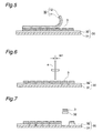
- Pressure sensitive adhesive sheet for pickup step 20 is stuck to the ground back of the semiconductor wafer.
- the pressure sensitive adhesive sheet for pickup step 20 comprises base 21 and, superimposed thereon, energy radiation curable pressure sensitive adhesive layer 22.
- the energy radiation polymerizable compound for use in the energy radiation curable pressure sensitive adhesive there can widely be employed low-molecular-weight compounds having at least two photopolymerizable carbon to carbon double bonds in each molecule thereof which can provide a three-dimensional network structure by light irradiation, as disclosed in, for example, Japanese Patent Laid-open Publication Nos. 60(1985)-196956 and 60(1985)-223139.
- the energy radiation curable pressure sensitive adhesive may be composed of an energy radiation curable copolymer having energy radiation polymerizable groups as side chains. Details of such an energy radiation curable copolymer are described in, for example, Japanese Patent Laid-open Publication Nos. 5(1993)-32946 and 8(1996)-27239.
- UV rays are used as the energy radiation.
- Ultraviolet rays are especially preferably employed. Exposure to energy radiation is performed on the side of base 21. Therefore, when ultraviolet rays are used as the energy radiation, the base 21 must be transparent.
- the surface protective sheet 10 is peeled (see Fig. 4).
- the energy radiation curable pressure sensitive adhesive layer 22 of the pressure sensitive adhesive sheet for pickup step 20 is cured by exposure to energy radiation in the above fifth step to thereby exhibit strong resistance to any lateral shear force. Therefore, after the curing of the energy radiation curable pressure sensitive adhesive layer 22 of the pressure sensitive adhesive sheet for pickup step 20, misregistration of chips would not be caused by the peeling of the surface protective sheet 10 to thereby enable maintaining an alignment of chips. Moreover, the adhesive strength is extremely reduced, vertical peeling of chips can be easily performed. At the peeling of the surface protective sheet 10, it is preferred to fix, by suction, the side of pressure sensitive adhesive sheet for pickup step 20.
- the first to third steps thereof are the same as in the above first process.
- the dicing/die bond sheet 30 comprises base 31 and, superimposed thereon, adhesive layer 32.
- the adhesive layer 32 is so formed as to be detachable from the base 31.
- the adhesive layer 32 adheres to the chips 3 at room temperature or under mild thermo-press bonding conditions. When the chips 3 are picked up after the application of the adhesive layer 32 to the chips 3, the adhesive layer 32 remains adhering to the back of the chips 3 and is detached from the base 31.
- dicing/die bond sheets including an adhesive layer containing an energy radiation curable pressure sensitive adhesive component and a thermosetting adhesive component as essential components, as described in, for example, Japanese Patent Laid-open Publication Nos. 2(1990)-32181, 8(1996)-53655, 8(1996)-239639, 9(1997)-100450 and 9(1997)-202872.
- the adhesive layer 32 is subjected to primary curing.
- dicing/die bond sheets including an adhesive layer containing an energy radiation curable pressure sensitive adhesive component and a thermosetting adhesive component as essential components, only the energy radiation curable pressure sensitive adhesive component can be cured (primary curing) by exposure to energy radiation.
- the primary curing of the adhesive layer 32 enables avoiding the misregistration of chips in the following fifth step.
- the timing of peeling the surface protective sheet 10 in the second process of the present invention is not particularly limited.
- the peeling of the surface protective sheet 10 may be carried out at any of the following fifth to seventh steps.
- the depth of cut is satisfactory as long as the adhesive layer 32 can be fully cut, it is generally preferred that the cutting be performed to such an extent that the base 31 is partially cut to thereby complete the splitting of the adhesive layer 32 into pieces. As a result, the adhesive layer 32 is cut into pieces of substantially the same size and shape as those of the chips 3.
- the fifth step is carried out while the surface protective sheet 10 remains stuck to the wafer circuit surface, it is preferred to employ a transparent surface protective sheet in order to ascertain dicing lines.
- the adhesive layer 32 together with the chips 3 is detached from the base 31 of the dicing/die bond sheet 30.
- the adhesive layer 32 as aforementioned, is so formed as to be detachable from the base 31. Accordingly, when the chips 3 are picked up, the adhesive layer 32 remains adhering to the back of the chips 3 and is detached from the base 31.
- the adhesive layer 32 is constituted of the aforementioned adhesive containing an energy radiation curable pressure sensitive adhesive component and a thermosetting adhesive component as essential components, primary curing of the adhesive layer 32 is effected by exposure to energy radiation in the above fourth step with the result that the adhesive strength of the adhesive layer 32 is lowered. Therefore, the peeling of the adhesive layer 32 from the base 31 can be effectively accomplished.
- the individual chips 3 are bonded through the adhesive layer 32 to a given substrate (not shown).
- the back of the chips 3 is furnished with the adhesive layer 32 in the above step 6.
- the chips 3 can be secured onto a substrate by disposing the chips 3 through the adhesive layer 32 on the substrate and by causing the adhesive layer 32 to exert its adhesive strength by required means.
- the adhesive layer 32 is composed of the aforementioned adhesive containing an energy radiation curable pressure sensitive adhesive component and a thermosetting adhesive component as essential components, the bonding capability of the thermosetting adhesive component can be exerted by heating to thereby enable strongly bonding the chips 3 and the substrate to each other.
- the first to third steps thereof are the same as in the above first process.
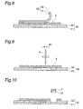
- die bond sheet 40 is stuck onto the ground back of the wafer.
- the die bond sheet 40 comprises base 41 and, superimposed thereon, thermoplastic adhesive layer 42.
- the thermoplastic adhesive layer 42 is so formed as to be detachable from the base 41.
- the thermoplastic adhesive layer 42 can be adhered to the chips 3 under mild thermo-press bonding conditions. When the chips 3 are picked up after the adhering of the thermoplastic adhesive layer 42 to the chips 3, the thermoplastic adhesive layer 42 remains adhering to the back of the chips 3 and is detached from the base 41.
- the thermoplastic adhesive layer 42 is constituted of, for example, any of polyester resins, polyvinyl acetate, polyvinyl alcohol, polyvinylbutyral, polyvinyl chloride, polymethacrylates, polyacrylates, polystyrene, polyethylene, polyamides, cellulose, polyisobutylene, polyvinyl ether, polyimide resins and various hot melt adhesives.
- the thermoplastic adhesive layer 42 is preferably comprising polyester resins or polyimide resins.
- the die bond sheet 40 After the thermo-press bonding of the above die bond sheet 40 to the ground back of the wafer, the die bond sheet 40 is allowed to cool.
- the cooling of the adhesive layer 42 enables avoiding the misregistration of chips in the following fifth step.
- the timing of peeling the surface protective sheet 10 is not particularly limited as similar to the above second process.
- the peeling of the surface protective sheet 10 may be carried out at any of the following fifth to seventh steps.
- the adhesive layer 42 is fully cut by means of dicing blade 4.
- the die bond sheet 40 be fixed on a suction table.
- the width W1 of the dicing blade 4, cut depth, etc. are the same as in the above second process.
- the fifth step is carried out while the surface protective sheet 10 remains stuck to the wafer circuit surface, it is preferred to employ a transparent surface protective sheet in order to ascertain dicing lines.
- the adhesive layer 42 together with the chips 3 is detached from the base 41 of the die bond sheet 40.
- the adhesive layer 42 as aforementioned, is so formed as to be detachable from the base 41. Accordingly, when the chips 3 are picked up, the adhesive layer 42 remains adhering to the back of the chips 3 and is detached from the base 41.
- the individual chips 3 are bonded through the adhesive layer 42 to a given substrate (not shown).
- the back of the chips 3 is furnished with the thermoplastic adhesive layer 42 in the above step 6.
- the chips 3 can be strongly secured onto the substrate by disposing the chips 3 on the substrate and by effecting a thermo-press bonding thereof.
- the second and third processes for producing a semiconductor device according to the present invention enable easily forming an appropriate amount of adhesive layer on the back of extremely thin chips to thereby enable avoiding chip breakage, chip cracking or package cracking while ensuring excellent chip alignment, so that a productivity enhancement can be realized.
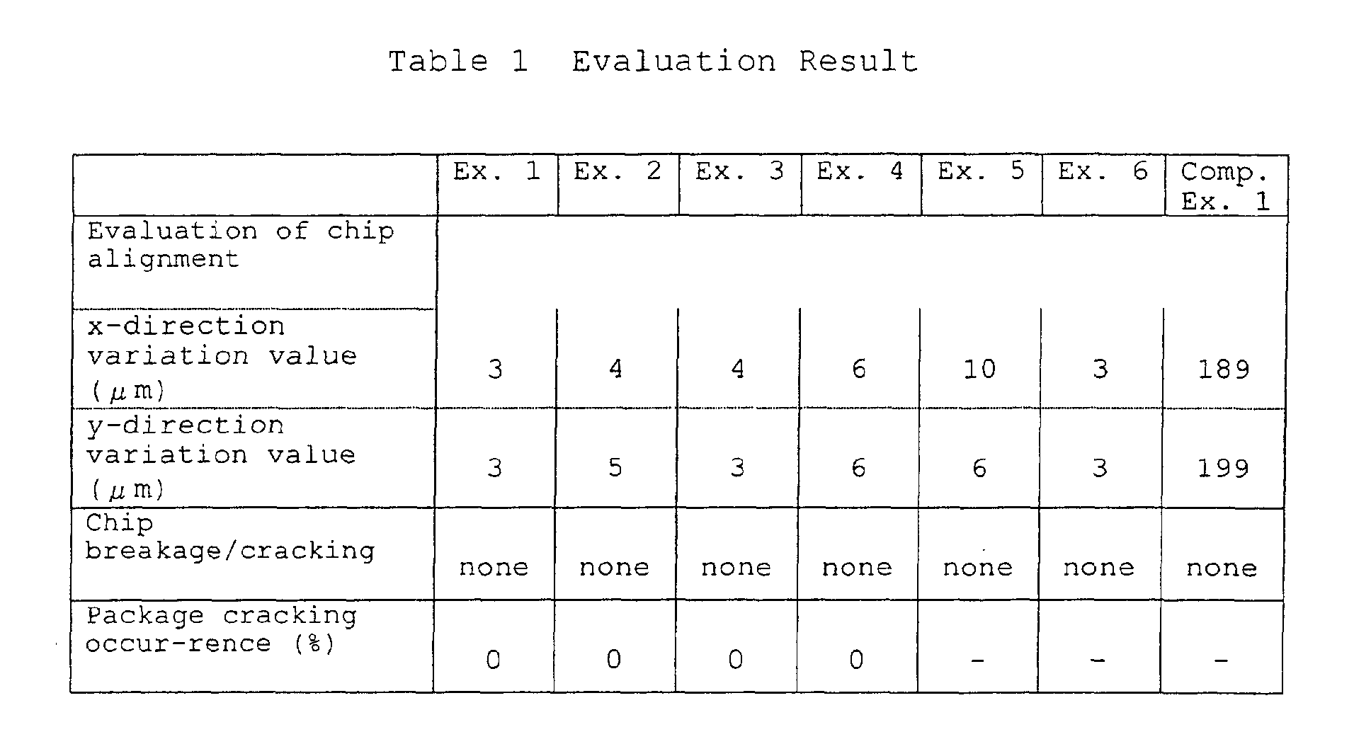
- Grooves were formed in the parallel direction (x-direction) and the perpendicular direction (y-direction) to an orientation flat of wafer. Dislocations between the positions of grooves at intersecting points (8 points) formed by mutual crossings of the fifth grooves up, down, right and left from the center of the wafer, among the intersecting points of x-direction grooves and y-direction grooves, and the positions of inter-chip lines corresponding to the above grooves after the division into chips were measured by means of wafer dicer (model A-WD-4000B, manufactured by Tokyo Seimitsu) with the use of alignment function thereof. The maximum of the x-direction and y-direction dislocations was expressed as the variation, whereby the chip alignment was evaluated.
- Silicon chips secured to a lead frame produced in the following Examples 1 to 4, were sealed under high pressure with the use of given sealant resin (biphenyl epoxy resin). The resin was cured at 175°C for 6 hr. In this manner, 100 packages for the package crack test were obtained. Each of the packages was allowed to stand still at high temperature in high humidity (85°C, 85% RH) for 168 hr. Thereafter, each package was allowed to stand still for 1 min in the same environment (215°C) as in VPS (Vapor Phase Soldering), and cooled to room temperature. These were carried out thrice, and any cracking of the sealant resin was inspected by SAT (Scanning Acoustic Tomography). The package cracking ratio is a proportion of the number of cracked packages to the number of inspected packages (namely 100).
- Grooves were formed on a silicon wafer of 6 inch diameter and 625 ⁇ m thickness by the use of the above wafer dicing machine using a 35 ⁇ m thick blade under conditions such that the cut depth was 150 ⁇ m and the chip size was 10 mm-square. Subsequently, the above surface protective sheet was stuck to the grooved surface of the silicon wafer and exposed to ultraviolet light. The back of the silicon wafer was ground by means of the above back grinding machine until the wafer thickness became 80 ⁇ m to thereby effect division of the silicon wafer into individual chips. Thereafter, dicing/die bond sheet (Adwill LE5000 produced by LINTEC Corporation) was stuck to the ground back of the silicon wafer.
- Adwill LE5000 produced by LINTEC Corporation
- the dicing/die bond sheet was exposed to ultraviolet light, thereby effecting a primary curing of the adhesive layer of the dicing/die bond sheet.
- the surface protective sheet was peeled off, and the adhesive layer lying between neighboring divided individual silicon chips was cut by the use of the wafer dicing machine using a 30 ⁇ m thick blade under conditions such that the cut depth was 35 ⁇ m. After this operation, the chip alignment thereof was evaluated.
- the divided individual silicon chips were picked up from the dicing/die bond sheet, and the silicon chips having the adhesive layer were directly bonded to die pad portions of a lead frame.
- the adhesive layer was heated at 160°C for 30 min, thereby effecting a secondary curing of the adhesive layer. Thus, bonding of the chips was accomplished.
- Grooves were formed on a silicon wafer of 6 inch diameter and 625 ⁇ m thickness by the use of the above wafer dicing machine using a 35 ⁇ m thick blade under conditions such that the cut depth was 150 ⁇ m and the chip size was 10 mm-square. Subsequently, the above surface protective sheet was stuck to the grooved surface of the silicon wafer and exposed to ultraviolet light. The back of the silicon wafer was ground by means of the above back grinding machine until the wafer thickness became 80 ⁇ m to thereby effect division of the silicon wafer into individual chips. Thereafter, dicing/die bond sheet (Adwill LE5000 produced by LINTEC Corporation) was stuck to the ground back of the silicon wafer.
- Adwill LE5000 produced by LINTEC Corporation
- the dicing/die bond sheet was exposed to ultraviolet light, thereby effecting a primary curing of the adhesive layer of the dicing/die bond sheet. Then, the side of dicing/die bond sheet was fixed on a suction table, and the surface protective sheet was peeled off.
- the adhesive layer lying between neighboring divided individual silicon chips was cut by the use of the wafer dicing machine using a 30 ⁇ m thick blade under conditions such that the cut depth was 65 ⁇ m. After this operation, the chip alignment thereof was evaluated.
- the divided individual silicon chips were picked up from the dicing/die bond sheet, and the silicon chips having the adhesive layer were directly bonded to die pad portions of a lead frame.
- the adhesive layer was heated at 160°C for 30 min, thereby effecting a secondary curing of the adhesive layer. Thus, bonding of the chips was accomplished.
- Grooves were formed on a silicon wafer of 6 inch diameter and 625 ⁇ m thickness by the use of the above wafer dicing machine using a 35 ⁇ m thick blade under conditions such that the cut depth was 150 ⁇ m and the chip size was 10 mm-square. Subsequently, the above surface protective sheet was stuck to the grooved surface of the silicon wafer and exposed to ultraviolet light. The back of the silicon wafer was ground by means of the above back grinding machine until the wafer thickness became 80 ⁇ m to thereby effect division of the silicon wafer into individual chips. Thereafter, dicing/die bond sheet (Adwill LE5000 produced by LINTEC Corporation) was stuck to the ground back of the silicon wafer.
- Adwill LE5000 produced by LINTEC Corporation
- the dicing/die bond sheet was exposed to ultraviolet light, thereby effecting a primary curing of the adhesive layer of the dicing/die bond sheet. Then, the adhesive layer lying between neighboring divided individual silicon chips, together with the surface protective sheet, was cut by the use of the wafer dicing machine using a 30 ⁇ m thick blade under conditions such that the cut depth was 65 ⁇ m. After this operation, the chip alignment thereof was evaluated.
- the surface protective sheet was peeled off.
- the divided individual silicon chips were picked up from the dicing/die bond sheet, and the silicon chips having the adhesive layer were directly bonded to die pad portions of a lead frame.
- the adhesive layer was heated at 160°C for 30 min, thereby effecting a secondary curing of the adhesive layer. Thus, bonding of the chips was accomplished.
Landscapes
- Mechanical Treatment Of Semiconductor (AREA)
- Dicing (AREA)
- Die Bonding (AREA)
Abstract
Description
semiconductor device in which not only can an appropriate amount of adhesive layer be easily formed on the back of extremely thin chips to thereby enable avoiding chip breakage, chip cracking or package cracking but also excellent chip alignment can be realized, so that a productivity enhancement can be realized.
for producing a semiconductor device which realizes excellent chip alignment to thereby enable improving a pickup efficiency. It is another object of the present invention at least in preferred embodiments to provide a process for producing a
semiconductor device in which an appropriate amount of adhesive layer can easily be formed on the back of extremely thin chips to thereby enable avoiding chip breakage, chip cracking or package cracking, so that a productivity enhancement can be realized.
Claims (4)
- A process for producing a semiconductor device, comprising the steps of:providing a wafer of given thickness having a surface furnished with semiconductor circuits and a back;forming grooves of a cut depth smaller than the thickness of the wafer, said grooves extending from the wafer circuit surface;sticking a surface protective sheet onto the wafer circuit surface;grinding the back of the wafer so that the thickness of the wafer is reduced to thereby finally result in division of the wafer into individual chips with spaces therebetween;sticking a pressure sensitive adhesive sheet for a pickup step onto the ground back of the wafer, said pressure sensitive adhesive sheet for the pickup step comprising a base and, superimposed thereon, an energy radiation curable pressure sensitive adhesive layer;exposing the energy radiation curable pressure sensitive adhesive layer to an energy radiation; andpeeling the surface protective sheet from the wafer circuit surface.
- A process for producing a semiconductor device, comprising the steps of:providing a wafer of given thickness having a surface furnished with'semiconductor circuits and a back;forming grooves of a cut depth smaller than the thickness of the wafer, said grooves extending from the wafer circuit surface;sticking a surface protective sheet onto the wafer circuit surface;grinding the back of the wafer so that the thickness of the wafer is reduced to thereby finally result in division of the wafer into individual chips with spaces therebetween;sticking a dicing/die bond sheet onto the ground back of the wafer, said dicing/die bond sheet comprising a base and, superimposed thereon, an adhesive layer;performing a primary curing of the adhesive layer;cutting the adhesive layer of the dicing/die bond sheet between neighboring individual chips;detaching the individual chips having the cut adhesive layer adhering thereto from the base of the dicing/die bond sheet;attaching the individual chips through the adhesive layer to a given substrate; andperforming a secondary curing of the adhesive layer to thereby secure the individual chips to the substrate.
- A process for producing a semiconductor device, comprising the steps of:providing a wafer of given thickness having a surface furnished with semiconductor circuits and a back;forming grooves of a cut depth smaller than the thickness of the wafer, said grooves extending from the wafer circuit surface;sticking a surface protective sheet onto the wafer circuit surface;grinding the back of the wafer so that the thickness of the wafer is reduced to thereby finally result in division of the wafer into individual chips with spaces therebetween;sticking a die bond sheet onto the ground back of the wafer, said die bond sheet comprising a base and, superimposed thereon, a thermoplastic adhesive layer;cutting the thermoplastic adhesive layer of the die bond sheet between neighboring individual chips;detaching the individual chips having the cut thermoplastic adhesive layer adhering thereto from the base of the die bond sheet;attaching the individual chips through the thermoplastic adhesive layer to a given substrate; andheating the thermoplastic adhesive layer to thereby secure the individual chips to the substrate.
- A process as claimed in any of claims 1 to 3, wherein the surface protective sheet has an energy radiation curable pressure sensitive adhesive layer, and wherein the energy radiation curable pressure sensitive adhesive layer of the surface protective sheet is cured after the sticking of the surface protective sheet to the wafer circuit surface but before the grinding of the back of the wafer.
Applications Claiming Priority (2)
| Application Number | Priority Date | Filing Date | Title |
|---|---|---|---|
| JP2000262238 | 2000-08-31 | ||
| JP2000262238A JP3906962B2 (en) | 2000-08-31 | 2000-08-31 | Manufacturing method of semiconductor device |
Publications (3)
| Publication Number | Publication Date |
|---|---|
| EP1195809A2 true EP1195809A2 (en) | 2002-04-10 |
| EP1195809A3 EP1195809A3 (en) | 2003-12-17 |
| EP1195809B1 EP1195809B1 (en) | 2018-06-27 |
Family
ID=18749953
Family Applications (1)
| Application Number | Title | Priority Date | Filing Date |
|---|---|---|---|
| EP01307357.2A Expired - Lifetime EP1195809B1 (en) | 2000-08-31 | 2001-08-30 | Process for producing semiconductor device |
Country Status (8)
| Country | Link |
|---|---|
| US (1) | US6558975B2 (en) |
| EP (1) | EP1195809B1 (en) |
| JP (1) | JP3906962B2 (en) |
| KR (1) | KR100805520B1 (en) |
| CN (1) | CN1218382C (en) |
| MY (1) | MY117750A (en) |
| SG (1) | SG100750A1 (en) |
| TW (1) | TWI246143B (en) |
Cited By (8)
| Publication number | Priority date | Publication date | Assignee | Title |
|---|---|---|---|---|
| WO2004036642A1 (en) * | 2002-10-18 | 2004-04-29 | Disco Corporation | Semiconductor wafer protective device and semiconductor wafer treatment method |
| DE10312662A1 (en) * | 2003-01-10 | 2004-07-22 | Kabushiki Kaisha Toshiba | Semiconductor device manufacturing device and semiconductor device manufacturing method for forming semiconductor chips by dicing semiconductor wafers |
| WO2005083779A1 (en) * | 2004-02-25 | 2005-09-09 | Infineon Technologies Ag | Rear-coated thin semiconductor chip, and method for the production thereof |
| DE102004054147A1 (en) * | 2004-11-08 | 2006-02-23 | Infineon Technologies Ag | Adhesive layer of material that is selectively hardened is bonded to thin semiconductor wafers |
| DE102004058876B3 (en) * | 2004-12-06 | 2006-05-24 | Infineon Technologies Ag | Adhesive layer applying method for semiconductor wafer, involves taking off coated semiconductor chips with adhesive layer from non-hardened adhesive of foil under forcing bond bridge of semiconductor wafer material along separation slots |
| US7235425B2 (en) * | 2004-02-24 | 2007-06-26 | Kabushiki Kaisha Toshiba | Semiconductor device and fabrication method for the same |
| US20100051190A1 (en) * | 2004-12-09 | 2010-03-04 | Qimonda Ag | Method for applying an adhesive layer on thin cut semiconductor chips of semiconductor wafers |
| CN107431004A (en) * | 2015-11-09 | 2017-12-01 | 古河电气工业株式会社 | The one-piece type surface protection band of mask |
Families Citing this family (70)
| Publication number | Priority date | Publication date | Assignee | Title |
|---|---|---|---|---|
| JP4409014B2 (en) * | 1999-11-30 | 2010-02-03 | リンテック株式会社 | Manufacturing method of semiconductor device |
| US7878905B2 (en) * | 2000-02-22 | 2011-02-01 | Creative Kingdoms, Llc | Multi-layered interactive play experience |
| JP4669162B2 (en) * | 2001-06-28 | 2011-04-13 | 株式会社ディスコ | Semiconductor wafer dividing system and dividing method |
| US20030042615A1 (en) | 2001-08-30 | 2003-03-06 | Tongbi Jiang | Stacked microelectronic devices and methods of fabricating same |
| JP3745260B2 (en) * | 2001-10-02 | 2006-02-15 | ローム株式会社 | Manufacturing method of semiconductor device |
| JP2003124146A (en) * | 2001-10-11 | 2003-04-25 | Lintec Corp | Protective sheet peeling method and apparatus |
| JP2003152058A (en) * | 2001-11-13 | 2003-05-23 | Lintec Corp | Wafer transfer device |
| JP3553551B2 (en) * | 2002-01-11 | 2004-08-11 | 沖電気工業株式会社 | Method of manufacturing semiconductor device using semiconductor wafer |
| US6896760B1 (en) * | 2002-01-16 | 2005-05-24 | Micron Technology, Inc. | Fabrication of stacked microelectronic devices |
| US6709953B2 (en) * | 2002-01-31 | 2004-03-23 | Infineon Technologies Ag | Method of applying a bottom surface protective coating to a wafer, and wafer dicing method |
| JP2003234359A (en) * | 2002-02-08 | 2003-08-22 | Hitachi Ltd | Method for manufacturing semiconductor device |
| US6713366B2 (en) * | 2002-06-12 | 2004-03-30 | Intel Corporation | Method of thinning a wafer utilizing a laminated reinforcing layer over the device side |
| JP2004043695A (en) * | 2002-07-15 | 2004-02-12 | Sumitomo Bakelite Co Ltd | Die bonding adhesive, method of manufacturing semiconductor device using the same, and semiconductor device |
| US7042072B1 (en) * | 2002-08-02 | 2006-05-09 | Amkor Technology, Inc. | Semiconductor package and method of manufacturing the same which reduces warpage |
| DE10238444B4 (en) * | 2002-08-22 | 2011-05-12 | United Monolithic Semiconductors Gmbh | Method for producing isolated monolithically integrated semiconductor circuits |
| JP4159431B2 (en) * | 2002-11-15 | 2008-10-01 | 株式会社ルネサステクノロジ | Manufacturing method of semiconductor device |
| KR100486290B1 (en) * | 2002-12-23 | 2005-04-29 | 삼성전자주식회사 | Assembling method of semiconductor package and removal apparatus of protection tape in semiconductor process |
| TWI240965B (en) | 2003-02-28 | 2005-10-01 | Toshiba Corp | Semiconductor wafer dividing method and apparatus |
| JP4346333B2 (en) * | 2003-03-26 | 2009-10-21 | 新光電気工業株式会社 | Method for manufacturing multilayer circuit board incorporating semiconductor element |
| JP4599075B2 (en) * | 2003-03-26 | 2010-12-15 | 株式会社東芝 | Semiconductor manufacturing apparatus and semiconductor device manufacturing method |
| JP2004304066A (en) * | 2003-03-31 | 2004-10-28 | Renesas Technology Corp | Method for manufacturing semiconductor device |
| JP4494728B2 (en) * | 2003-05-26 | 2010-06-30 | 株式会社ディスコ | Non-metallic substrate division method |
| JP4093930B2 (en) * | 2003-07-17 | 2008-06-04 | 株式会社東京精密 | Frame transport prober |
| US20050023682A1 (en) * | 2003-07-31 | 2005-02-03 | Morio Nakao | High reliability chip scale package |
| JP4130167B2 (en) * | 2003-10-06 | 2008-08-06 | 日東電工株式会社 | Semiconductor wafer peeling method |
| JP4562118B2 (en) * | 2003-12-19 | 2010-10-13 | 日東電工株式会社 | Manufacturing method of semiconductor device |
| KR100696287B1 (en) * | 2004-01-28 | 2007-03-19 | 미쓰이 가가쿠 가부시키가이샤 | How to Protect Semiconductor Wafers |
| JP2005223244A (en) * | 2004-02-09 | 2005-08-18 | Tokyo Seimitsu Co Ltd | Tip pop-up position detection method |
| JP4514490B2 (en) * | 2004-03-29 | 2010-07-28 | 日東電工株式会社 | Semiconductor wafer fragmentation method |
| US20050249945A1 (en) * | 2004-05-10 | 2005-11-10 | Wen Kun Yang | Manufacturing tool for wafer level package and method of placing dies |
| TWI244731B (en) * | 2004-05-31 | 2005-12-01 | Advanced Semiconductor Eng | Method for improving balance of molding flow during assembling semiconductor packages with fail unit |
| JP3830497B2 (en) * | 2004-06-11 | 2006-10-04 | シャープ株式会社 | Semiconductor wafer manufacturing method and semiconductor device manufacturing method |
| JP2006019493A (en) * | 2004-07-01 | 2006-01-19 | Disco Abrasive Syst Ltd | Wafer dividing method |
| KR100574983B1 (en) * | 2004-07-06 | 2006-05-02 | 삼성전자주식회사 | Semiconductor Wafer Processing Method for Semiconductor Device Manufacturing |
| WO2006008795A1 (en) * | 2004-07-16 | 2006-01-26 | Shinko Electric Industries Co., Ltd. | Semiconductor device manufacturing method |
| DE102005015036B4 (en) * | 2004-07-19 | 2008-08-28 | Qimonda Ag | Method for mounting a chip on a substrate |
| DE102004048202B4 (en) | 2004-09-30 | 2008-05-21 | Infineon Technologies Ag | Method for separating surface-mountable semiconductor components and for equipping them with external contacts |
| WO2006047117A2 (en) * | 2004-10-21 | 2006-05-04 | Chippac, Inc. | Method for reducing semiconductor die warpage |
| US7169248B1 (en) * | 2005-07-19 | 2007-01-30 | Micron Technology, Inc. | Methods for releasably attaching support members to microfeature workpieces and microfeature assemblies formed using such methods |
| US7504318B2 (en) * | 2005-09-19 | 2009-03-17 | Intel Corporation | Nanopowder coating for scribing and structures formed thereby |
| JP4954569B2 (en) * | 2006-02-16 | 2012-06-20 | 日東電工株式会社 | Manufacturing method of semiconductor device |
| JP4799205B2 (en) * | 2006-02-16 | 2011-10-26 | 日東電工株式会社 | Active surface-attached dicing adhesive tape or sheet and method of picking up a workpiece cut piece |
| US7749349B2 (en) | 2006-03-14 | 2010-07-06 | Micron Technology, Inc. | Methods and systems for releasably attaching support members to microfeature workpieces |
| US20090001611A1 (en) * | 2006-09-08 | 2009-01-01 | Takeshi Matsumura | Adhesive sheet for manufacturing semiconductor device, manufacturing method of semiconductor device using the sheet, and semiconductor device obtained by the method |
| MY153208A (en) * | 2006-09-15 | 2015-01-29 | Lintec Corp | Process for manufacturing semiconductor devices |
| CN101477956B (en) * | 2008-01-04 | 2012-05-16 | 南茂科技股份有限公司 | Small chip reconfiguration packaging structure and packaging method |
| CN101488462B (en) * | 2008-01-15 | 2010-12-08 | 南茂科技股份有限公司 | Modular multi-die package structure and method thereof |
| JP2009231779A (en) * | 2008-03-25 | 2009-10-08 | Lintec Corp | Method of manufacturing semiconductor device |
| JP5583140B2 (en) * | 2008-12-02 | 2014-09-03 | アリゾナ・ボード・オブ・リージェンツ,フォー・アンド・オン・ビハーフ・オブ・アリゾナ・ステート・ユニバーシティ | Method for preparing flexible substrate assembly and flexible substrate assembly prepared by the method |
| JP2010206044A (en) * | 2009-03-05 | 2010-09-16 | Toshiba Corp | Method of manufacturing semiconductor device |
| US8173552B2 (en) * | 2009-08-04 | 2012-05-08 | Intel Corporation | Method of fabricating an identification mark utilizing a liquid film assisted by a laser |
| TWI401737B (en) * | 2009-12-08 | 2013-07-11 | Chipmos Technologies Inc | Wafer cutting method |
| WO2011132647A1 (en) * | 2010-04-19 | 2011-10-27 | 日東電工株式会社 | Film for back surface of flip-chip semiconductor |
| US8283742B2 (en) | 2010-08-31 | 2012-10-09 | Infineon Technologies, A.G. | Thin-wafer current sensors |
| CN102760699B (en) * | 2011-04-27 | 2014-11-05 | 无锡华润安盛科技有限公司 | Method of cutting wafer used for preparation of sensor chip into grains |
| JP6134507B2 (en) * | 2011-12-28 | 2017-05-24 | ローム株式会社 | Chip resistor and manufacturing method thereof |
| CN103219224B (en) * | 2012-01-20 | 2016-03-09 | 陈志豪 | Wafer fabrication process with environmentally friendly processing |
| JP6061590B2 (en) * | 2012-09-27 | 2017-01-18 | 株式会社ディスコ | Surface protection member and processing method |
| JP6026222B2 (en) * | 2012-10-23 | 2016-11-16 | 株式会社ディスコ | Wafer processing method |
| JP2015041687A (en) * | 2013-08-21 | 2015-03-02 | 株式会社ディスコ | Wafer processing method |
| WO2016003983A1 (en) | 2014-07-01 | 2016-01-07 | Isola Usa Corp. | Prepregs including uv curable resins useful for manufacturing semi-flexible pcbs |
| CN107112256A (en) * | 2014-12-29 | 2017-08-29 | 卡尔·海因茨·普利瓦西尔 | Protective sheet used in processing semiconductor-sized wafers and semiconductor-sized wafer processing method |
| JP6479532B2 (en) * | 2015-03-30 | 2019-03-06 | ルネサスエレクトロニクス株式会社 | Semiconductor device manufacturing method |
| US20170148955A1 (en) * | 2015-11-22 | 2017-05-25 | Cyntec Co., Ltd. | Method of wafer level packaging of a module |
| KR102155028B1 (en) * | 2016-03-31 | 2020-09-11 | 후루카와 덴키 고교 가부시키가이샤 | Mask-integrated surface protection tape |
| JP6782215B2 (en) * | 2017-10-18 | 2020-11-11 | 古河電気工業株式会社 | Manufacturing method of mask material for plasma dicing, mask-integrated surface protective tape and semiconductor chip |
| US11854856B2 (en) * | 2019-02-25 | 2023-12-26 | Mitsubishi Electric Corporation | Method of manufacturing semiconductor element |
| MY198402A (en) | 2020-12-17 | 2023-08-28 | Inari Tech Sdn Bhd | A Method For Fabricating Semiconductor Articles And System Thereof |
| KR102625710B1 (en) * | 2021-09-24 | 2024-01-16 | 주식회사 루츠 | A manufacturing method of a fluorescent substance |
| KR102837821B1 (en) * | 2022-05-24 | 2025-07-23 | 주식회사 루츠 | A manufacturing method of a fluorescent substance |
Family Cites Families (27)
| Publication number | Priority date | Publication date | Assignee | Title |
|---|---|---|---|---|
| JPS59121852A (en) * | 1982-12-27 | 1984-07-14 | Nec Home Electronics Ltd | Wafer dicing device |
| JPH0616524B2 (en) | 1984-03-12 | 1994-03-02 | 日東電工株式会社 | Adhesive thin plate for fixing semiconductor wafers |
| JPS60223139A (en) | 1984-04-18 | 1985-11-07 | Nitto Electric Ind Co Ltd | Bonding sheet for fixing semiconductor wafer |
| JPS61112345A (en) * | 1984-11-07 | 1986-05-30 | Toshiba Corp | Manufacture of semiconductor device |
| JPS624341A (en) * | 1985-06-29 | 1987-01-10 | Toshiba Corp | Manufacture of semiconductor device |
| JPH0715087B2 (en) | 1988-07-21 | 1995-02-22 | リンテック株式会社 | Adhesive tape and method of using the same |
| JPH03177050A (en) * | 1989-12-05 | 1991-08-01 | Fujitsu Ltd | Manufacture of semiconductor device |
| JP2601956B2 (en) | 1991-07-31 | 1997-04-23 | リンテック株式会社 | Removable adhesive polymer |
| US5762744A (en) * | 1991-12-27 | 1998-06-09 | Rohm Co., Ltd. | Method of producing a semiconductor device using an expand tape |
| JPH05335411A (en) | 1992-06-02 | 1993-12-17 | Toshiba Corp | Pellet manufacturing method |
| JP2984549B2 (en) | 1994-07-12 | 1999-11-29 | リンテック株式会社 | Energy ray-curable pressure-sensitive adhesive composition and method of using the same |
| JP3483161B2 (en) | 1994-08-11 | 2004-01-06 | リンテック株式会社 | Adhesive tape and method of using the same |
| JPH08239639A (en) | 1995-03-02 | 1996-09-17 | Sekisui Chem Co Ltd | Adhesive composition and adhesive processed product using the same |
| US6054372A (en) * | 1995-04-03 | 2000-04-25 | Aptek Industries, Inc. | Stress-free silicon wafer and a die or chip made therefrom |
| JP3467611B2 (en) * | 1995-09-29 | 2003-11-17 | 日本テキサス・インスツルメンツ株式会社 | Method for manufacturing semiconductor device |
| JPH09100450A (en) | 1995-10-03 | 1997-04-15 | Lintec Corp | Adhesive tape and method of using the same |
| JP4094080B2 (en) | 1995-11-22 | 2008-06-04 | リンテック株式会社 | Adhesive composition and adhesive sheet |
| US6083811A (en) * | 1996-02-07 | 2000-07-04 | Northrop Grumman Corporation | Method for producing thin dice from fragile materials |
| JPH1140520A (en) * | 1997-07-23 | 1999-02-12 | Toshiba Corp | Method of dividing wafer and method of manufacturing semiconductor device |
| JP3526731B2 (en) * | 1997-10-08 | 2004-05-17 | 沖電気工業株式会社 | Semiconductor device and manufacturing method thereof |
| JPH11305673A (en) | 1998-04-17 | 1999-11-05 | Nippon Columbia Co Ltd | Display device |
| JPH11340334A (en) | 1998-05-27 | 1999-12-10 | Hitachi Ltd | Semiconductor device and wiring correction method |
| JP3410371B2 (en) * | 1998-08-18 | 2003-05-26 | リンテック株式会社 | Surface protection sheet for wafer back grinding and method of using the same |
| DE19840508A1 (en) * | 1998-09-04 | 1999-12-02 | Siemens Ag | Separating individual semiconductor chips from composite wafer |
| JP3816253B2 (en) * | 1999-01-19 | 2006-08-30 | 富士通株式会社 | Manufacturing method of semiconductor device |
| JP3865184B2 (en) * | 1999-04-22 | 2007-01-10 | 富士通株式会社 | Manufacturing method of semiconductor device |
| JP2001156028A (en) * | 1999-11-30 | 2001-06-08 | Lintec Corp | Method for manufacturing semiconductor device |
-
2000
- 2000-08-31 JP JP2000262238A patent/JP3906962B2/en not_active Expired - Lifetime
-
2001
- 2001-08-25 SG SG200105149A patent/SG100750A1/en unknown
- 2001-08-29 TW TW090121256A patent/TWI246143B/en not_active IP Right Cessation
- 2001-08-29 KR KR1020010052331A patent/KR100805520B1/en not_active Expired - Lifetime
- 2001-08-30 US US09/943,488 patent/US6558975B2/en not_active Expired - Lifetime
- 2001-08-30 MY MYPI20014113A patent/MY117750A/en unknown
- 2001-08-30 EP EP01307357.2A patent/EP1195809B1/en not_active Expired - Lifetime
- 2001-08-31 CN CN011312696A patent/CN1218382C/en not_active Expired - Lifetime
Non-Patent Citations (1)
| Title |
|---|
| None |
Cited By (15)
| Publication number | Priority date | Publication date | Assignee | Title |
|---|---|---|---|---|
| US6943045B2 (en) | 2002-10-18 | 2005-09-13 | Disco Corporation | Semiconductor wafer protective device and semiconductor wafer treatment method |
| WO2004036642A1 (en) * | 2002-10-18 | 2004-04-29 | Disco Corporation | Semiconductor wafer protective device and semiconductor wafer treatment method |
| DE10312662B4 (en) * | 2003-01-10 | 2008-06-05 | Kabushiki Kaisha Toshiba | Semiconductor device manufacturing arrangement and semiconductor device manufacturing method for forming semiconductor chips by dividing semiconductor wafers |
| US7140951B2 (en) | 2003-01-10 | 2006-11-28 | Kabushiki Kaisha Toshiba | Semiconductor device manufacturing apparatus and semiconductor device manufacturing method for forming semiconductor chips by dividing semiconductor wafer |
| DE10312662A1 (en) * | 2003-01-10 | 2004-07-22 | Kabushiki Kaisha Toshiba | Semiconductor device manufacturing device and semiconductor device manufacturing method for forming semiconductor chips by dicing semiconductor wafers |
| US7235425B2 (en) * | 2004-02-24 | 2007-06-26 | Kabushiki Kaisha Toshiba | Semiconductor device and fabrication method for the same |
| WO2005083779A1 (en) * | 2004-02-25 | 2005-09-09 | Infineon Technologies Ag | Rear-coated thin semiconductor chip, and method for the production thereof |
| DE102004009742B4 (en) * | 2004-02-25 | 2010-03-04 | Infineon Technologies Ag | Method for producing back-coated semiconductor chips |
| DE102004054147A1 (en) * | 2004-11-08 | 2006-02-23 | Infineon Technologies Ag | Adhesive layer of material that is selectively hardened is bonded to thin semiconductor wafers |
| DE102004058876B3 (en) * | 2004-12-06 | 2006-05-24 | Infineon Technologies Ag | Adhesive layer applying method for semiconductor wafer, involves taking off coated semiconductor chips with adhesive layer from non-hardened adhesive of foil under forcing bond bridge of semiconductor wafer material along separation slots |
| WO2006060976A1 (en) * | 2004-12-06 | 2006-06-15 | Qimonda Ag | Method for applying an adhesive layer to thinly ground semiconductor chips of a semiconductor wafer |
| US8580070B2 (en) | 2004-12-06 | 2013-11-12 | Edward Fuergut | Method of applying an adhesive layer on thincut semiconductor chips of a semiconductor wafer |
| US20100051190A1 (en) * | 2004-12-09 | 2010-03-04 | Qimonda Ag | Method for applying an adhesive layer on thin cut semiconductor chips of semiconductor wafers |
| CN107431004A (en) * | 2015-11-09 | 2017-12-01 | 古河电气工业株式会社 | The one-piece type surface protection band of mask |
| US11707804B2 (en) | 2015-11-09 | 2023-07-25 | Furukawa Electric Co., Ltd. | Mask-integrated surface protective tape |
Also Published As
| Publication number | Publication date |
|---|---|
| TWI246143B (en) | 2005-12-21 |
| KR100805520B1 (en) | 2008-02-20 |
| MY117750A (en) | 2004-07-31 |
| US6558975B2 (en) | 2003-05-06 |
| US20020055238A1 (en) | 2002-05-09 |
| CN1340855A (en) | 2002-03-20 |
| KR20020018084A (en) | 2002-03-07 |
| SG100750A1 (en) | 2003-12-26 |
| CN1218382C (en) | 2005-09-07 |
| JP2002075921A (en) | 2002-03-15 |
| EP1195809B1 (en) | 2018-06-27 |
| JP3906962B2 (en) | 2007-04-18 |
| EP1195809A3 (en) | 2003-12-17 |
Similar Documents
| Publication | Publication Date | Title |
|---|---|---|
| US6558975B2 (en) | Process for producing semiconductor device | |
| US6656819B1 (en) | Process for producing semiconductor device | |
| US7294531B2 (en) | Wafer level chip stack method | |
| US6312800B1 (en) | Pressure sensitive adhesive sheet for producing a chip | |
| CN100517564C (en) | Fabrication method of semiconductor circuit device | |
| EP0828292B1 (en) | Manufacture of a semiconductor device | |
| US7833836B2 (en) | Stack MCP and manufacturing method thereof | |
| JPH11204551A (en) | Method for manufacturing semiconductor device | |
| JPH0997806A (en) | Semiconductor device, manufacturing method thereof, and adhesive member for dicing | |
| US6995468B2 (en) | Semiconductor apparatus utilizing a preparatory stage for a chip assembly | |
| US20070023136A1 (en) | Method for processing a semiconductor wafer | |
| JP2005209940A (en) | Method for manufacturing semiconductor device | |
| JP4394109B2 (en) | Manufacturing method of semiconductor device | |
| US20070057410A1 (en) | Method of fabricating wafer chips | |
| JP2001156028A (en) | Method for manufacturing semiconductor device | |
| JP3819378B2 (en) | Adhesive sheet for chip body manufacturing | |
| HK1035261B (en) | Method for producing semiconductor device | |
| CN103460361B (en) | Dicing tape is applied with the wafer of the precut of bottom filling film | |
| JP2003086538A (en) | Method for manufacturing semiconductor chip | |
| CN103460361A (en) | Pre-cut wafer applied underfill film on dicing tape |
Legal Events
| Date | Code | Title | Description |
|---|---|---|---|
| PUAI | Public reference made under article 153(3) epc to a published international application that has entered the european phase |
Free format text: ORIGINAL CODE: 0009012 |
|
| AK | Designated contracting states |
Kind code of ref document: A2 Designated state(s): AT BE CH CY DE DK ES FI FR GB GR IE IT LI LU MC NL PT SE TR |
|
| AX | Request for extension of the european patent |
Free format text: AL;LT;LV;MK;RO;SI |
|
| PUAL | Search report despatched |
Free format text: ORIGINAL CODE: 0009013 |
|
| AK | Designated contracting states |
Kind code of ref document: A3 Designated state(s): AT BE CH CY DE DK ES FI FR GB GR IE IT LI LU MC NL PT SE TR |
|
| AX | Request for extension of the european patent |
Extension state: AL LT LV MK RO SI |
|
| 17P | Request for examination filed |
Effective date: 20040614 |
|
| AKX | Designation fees paid |
Designated state(s): DE FR GB IT NL |
|
| 17Q | First examination report despatched |
Effective date: 20040805 |
|
| GRAP | Despatch of communication of intention to grant a patent |
Free format text: ORIGINAL CODE: EPIDOSNIGR1 |
|
| STAA | Information on the status of an ep patent application or granted ep patent |
Free format text: STATUS: GRANT OF PATENT IS INTENDED |
|
| RIC1 | Information provided on ipc code assigned before grant |
Ipc: H01L 23/00 20060101ALI20171130BHEP Ipc: H01L 21/683 20060101ALI20171130BHEP Ipc: H01L 21/78 20060101AFI20171130BHEP |
|
| INTG | Intention to grant announced |
Effective date: 20180103 |
|
| GRAS | Grant fee paid |
Free format text: ORIGINAL CODE: EPIDOSNIGR3 |
|
| GRAA | (expected) grant |
Free format text: ORIGINAL CODE: 0009210 |
|
| STAA | Information on the status of an ep patent application or granted ep patent |
Free format text: STATUS: THE PATENT HAS BEEN GRANTED |
|
| AK | Designated contracting states |
Kind code of ref document: B1 Designated state(s): DE FR GB IT NL |
|
| REG | Reference to a national code |
Ref country code: GB Ref legal event code: FG4D |
|
| REG | Reference to a national code |
Ref country code: DE Ref legal event code: R096 Ref document number: 60150869 Country of ref document: DE |
|
| REG | Reference to a national code |
Ref country code: NL Ref legal event code: FP |
|
| REG | Reference to a national code |
Ref country code: FR Ref legal event code: PLFP Year of fee payment: 18 |
|
| RIC2 | Information provided on ipc code assigned after grant |
Ipc: H01L 21/78 20060101AFI20171130BHEP Ipc: H01L 21/683 20060101ALI20171130BHEP Ipc: H01L 23/00 20060101ALI20171130BHEP |
|
| REG | Reference to a national code |
Ref country code: DE Ref legal event code: R097 Ref document number: 60150869 Country of ref document: DE |
|
| PLBE | No opposition filed within time limit |
Free format text: ORIGINAL CODE: 0009261 |
|
| STAA | Information on the status of an ep patent application or granted ep patent |
Free format text: STATUS: NO OPPOSITION FILED WITHIN TIME LIMIT |
|
| 26N | No opposition filed |
Effective date: 20190328 |
|
| PGFP | Annual fee paid to national office [announced via postgrant information from national office to epo] |
Ref country code: GB Payment date: 20200826 Year of fee payment: 20 Ref country code: FR Payment date: 20200821 Year of fee payment: 20 Ref country code: NL Payment date: 20200826 Year of fee payment: 20 Ref country code: DE Payment date: 20200819 Year of fee payment: 20 |
|
| PGFP | Annual fee paid to national office [announced via postgrant information from national office to epo] |
Ref country code: IT Payment date: 20200826 Year of fee payment: 20 |
|
| REG | Reference to a national code |
Ref country code: DE Ref legal event code: R071 Ref document number: 60150869 Country of ref document: DE |
|
| REG | Reference to a national code |
Ref country code: NL Ref legal event code: MK Effective date: 20210829 |
|
| REG | Reference to a national code |
Ref country code: GB Ref legal event code: PE20 Expiry date: 20210829 |
|
| PG25 | Lapsed in a contracting state [announced via postgrant information from national office to epo] |
Ref country code: GB Free format text: LAPSE BECAUSE OF EXPIRATION OF PROTECTION Effective date: 20210829 |