EP1195801A2 - Verfahren zur Behandlung einer Isolierschicht mit niedriger Dielektrizitätskonstante - Google Patents
Verfahren zur Behandlung einer Isolierschicht mit niedriger Dielektrizitätskonstante Download PDFInfo
- Publication number
- EP1195801A2 EP1195801A2 EP01870205A EP01870205A EP1195801A2 EP 1195801 A2 EP1195801 A2 EP 1195801A2 EP 01870205 A EP01870205 A EP 01870205A EP 01870205 A EP01870205 A EP 01870205A EP 1195801 A2 EP1195801 A2 EP 1195801A2
- Authority
- EP
- European Patent Office
- Prior art keywords
- low
- plasma
- layer
- substrate
- opening
- Prior art date
- Legal status (The legal status is an assumption and is not a legal conclusion. Google has not performed a legal analysis and makes no representation as to the accuracy of the status listed.)
- Granted
Links
Images






Classifications
-
- H—ELECTRICITY
- H10—SEMICONDUCTOR DEVICES; ELECTRIC SOLID-STATE DEVICES NOT OTHERWISE PROVIDED FOR
- H10P—GENERIC PROCESSES OR APPARATUS FOR THE MANUFACTURE OR TREATMENT OF DEVICES COVERED BY CLASS H10
- H10P50/00—Etching of wafers, substrates or parts of devices
- H10P50/20—Dry etching; Plasma etching; Reactive-ion etching
- H10P50/28—Dry etching; Plasma etching; Reactive-ion etching of insulating materials
- H10P50/282—Dry etching; Plasma etching; Reactive-ion etching of insulating materials of inorganic materials
- H10P50/283—Dry etching; Plasma etching; Reactive-ion etching of insulating materials of inorganic materials by chemical means
-
- H—ELECTRICITY
- H10—SEMICONDUCTOR DEVICES; ELECTRIC SOLID-STATE DEVICES NOT OTHERWISE PROVIDED FOR
- H10P—GENERIC PROCESSES OR APPARATUS FOR THE MANUFACTURE OR TREATMENT OF DEVICES COVERED BY CLASS H10
- H10P14/00—Formation of materials, e.g. in the shape of layers or pillars
- H10P14/60—Formation of materials, e.g. in the shape of layers or pillars of insulating materials
- H10P14/66—Formation of materials, e.g. in the shape of layers or pillars of insulating materials characterised by the type of materials
- H10P14/665—Porous materials
-
- H—ELECTRICITY
- H10—SEMICONDUCTOR DEVICES; ELECTRIC SOLID-STATE DEVICES NOT OTHERWISE PROVIDED FOR
- H10P—GENERIC PROCESSES OR APPARATUS FOR THE MANUFACTURE OR TREATMENT OF DEVICES COVERED BY CLASS H10
- H10P14/00—Formation of materials, e.g. in the shape of layers or pillars
- H10P14/60—Formation of materials, e.g. in the shape of layers or pillars of insulating materials
- H10P14/65—Formation of materials, e.g. in the shape of layers or pillars of insulating materials characterised by treatments performed before or after the formation of the materials
- H10P14/6516—Formation of materials, e.g. in the shape of layers or pillars of insulating materials characterised by treatments performed before or after the formation of the materials of treatments performed after formation of the materials
- H10P14/6529—Formation of materials, e.g. in the shape of layers or pillars of insulating materials characterised by treatments performed before or after the formation of the materials of treatments performed after formation of the materials by exposure to a gas or vapour
- H10P14/6532—Formation of materials, e.g. in the shape of layers or pillars of insulating materials characterised by treatments performed before or after the formation of the materials of treatments performed after formation of the materials by exposure to a gas or vapour by exposure to a plasma
-
- H—ELECTRICITY
- H10—SEMICONDUCTOR DEVICES; ELECTRIC SOLID-STATE DEVICES NOT OTHERWISE PROVIDED FOR
- H10P—GENERIC PROCESSES OR APPARATUS FOR THE MANUFACTURE OR TREATMENT OF DEVICES COVERED BY CLASS H10
- H10P14/00—Formation of materials, e.g. in the shape of layers or pillars
- H10P14/60—Formation of materials, e.g. in the shape of layers or pillars of insulating materials
- H10P14/69—Inorganic materials
- H10P14/6903—Inorganic materials containing silicon
- H10P14/6905—Inorganic materials containing silicon being a silicon carbide or silicon carbonitride and not containing oxygen, e.g. SiC or SiC:H
-
- H—ELECTRICITY
- H10—SEMICONDUCTOR DEVICES; ELECTRIC SOLID-STATE DEVICES NOT OTHERWISE PROVIDED FOR
- H10P—GENERIC PROCESSES OR APPARATUS FOR THE MANUFACTURE OR TREATMENT OF DEVICES COVERED BY CLASS H10
- H10P14/00—Formation of materials, e.g. in the shape of layers or pillars
- H10P14/60—Formation of materials, e.g. in the shape of layers or pillars of insulating materials
- H10P14/69—Inorganic materials
- H10P14/692—Inorganic materials composed of oxides, glassy oxides or oxide-based glasses
- H10P14/6921—Inorganic materials composed of oxides, glassy oxides or oxide-based glasses containing silicon
- H10P14/6922—Inorganic materials composed of oxides, glassy oxides or oxide-based glasses containing silicon the material containing Si, O and at least one of H, N, C, F or other non-metal elements, e.g. SiOC, SiOC:H or SiONC
-
- H—ELECTRICITY
- H10—SEMICONDUCTOR DEVICES; ELECTRIC SOLID-STATE DEVICES NOT OTHERWISE PROVIDED FOR
- H10W—GENERIC PACKAGES, INTERCONNECTIONS, CONNECTORS OR OTHER CONSTRUCTIONAL DETAILS OF DEVICES COVERED BY CLASS H10
- H10W20/00—Interconnections in chips, wafers or substrates
- H10W20/01—Manufacture or treatment
- H10W20/071—Manufacture or treatment of dielectric parts thereof
- H10W20/074—Manufacture or treatment of dielectric parts thereof of dielectric parts comprising thin functional dielectric layers, e.g. dielectric etch-stop, barrier, capping or liner layers
- H10W20/076—Manufacture or treatment of dielectric parts thereof of dielectric parts comprising thin functional dielectric layers, e.g. dielectric etch-stop, barrier, capping or liner layers in via holes or trenches
-
- H—ELECTRICITY
- H10—SEMICONDUCTOR DEVICES; ELECTRIC SOLID-STATE DEVICES NOT OTHERWISE PROVIDED FOR
- H10W—GENERIC PACKAGES, INTERCONNECTIONS, CONNECTORS OR OTHER CONSTRUCTIONAL DETAILS OF DEVICES COVERED BY CLASS H10
- H10W20/00—Interconnections in chips, wafers or substrates
- H10W20/01—Manufacture or treatment
- H10W20/071—Manufacture or treatment of dielectric parts thereof
- H10W20/081—Manufacture or treatment of dielectric parts thereof by forming openings in the dielectric parts
-
- H—ELECTRICITY
- H10—SEMICONDUCTOR DEVICES; ELECTRIC SOLID-STATE DEVICES NOT OTHERWISE PROVIDED FOR
- H10W—GENERIC PACKAGES, INTERCONNECTIONS, CONNECTORS OR OTHER CONSTRUCTIONAL DETAILS OF DEVICES COVERED BY CLASS H10
- H10W20/00—Interconnections in chips, wafers or substrates
- H10W20/01—Manufacture or treatment
- H10W20/071—Manufacture or treatment of dielectric parts thereof
- H10W20/093—Manufacture or treatment of dielectric parts thereof by modifying materials of the dielectric parts
- H10W20/096—Manufacture or treatment of dielectric parts thereof by modifying materials of the dielectric parts by contacting with gases, liquids or plasmas
-
- H—ELECTRICITY
- H10—SEMICONDUCTOR DEVICES; ELECTRIC SOLID-STATE DEVICES NOT OTHERWISE PROVIDED FOR
- H10P—GENERIC PROCESSES OR APPARATUS FOR THE MANUFACTURE OR TREATMENT OF DEVICES COVERED BY CLASS H10
- H10P14/00—Formation of materials, e.g. in the shape of layers or pillars
- H10P14/60—Formation of materials, e.g. in the shape of layers or pillars of insulating materials
- H10P14/63—Formation of materials, e.g. in the shape of layers or pillars of insulating materials characterised by the formation processes
- H10P14/6326—Deposition processes
- H10P14/6328—Deposition from the gas or vapour phase
- H10P14/6334—Deposition from the gas or vapour phase using decomposition or reaction of gaseous or vapour phase compounds, i.e. chemical vapour deposition
- H10P14/6336—Deposition from the gas or vapour phase using decomposition or reaction of gaseous or vapour phase compounds, i.e. chemical vapour deposition in the presence of a plasma [PECVD]
-
- H—ELECTRICITY
- H10—SEMICONDUCTOR DEVICES; ELECTRIC SOLID-STATE DEVICES NOT OTHERWISE PROVIDED FOR
- H10P—GENERIC PROCESSES OR APPARATUS FOR THE MANUFACTURE OR TREATMENT OF DEVICES COVERED BY CLASS H10
- H10P14/00—Formation of materials, e.g. in the shape of layers or pillars
- H10P14/60—Formation of materials, e.g. in the shape of layers or pillars of insulating materials
- H10P14/66—Formation of materials, e.g. in the shape of layers or pillars of insulating materials characterised by the type of materials
- H10P14/668—Formation of materials, e.g. in the shape of layers or pillars of insulating materials characterised by the type of materials the materials being characterised by the deposition precursor materials
- H10P14/6681—Formation of materials, e.g. in the shape of layers or pillars of insulating materials characterised by the type of materials the materials being characterised by the deposition precursor materials the precursor containing a compound comprising Si
- H10P14/6684—Formation of materials, e.g. in the shape of layers or pillars of insulating materials characterised by the type of materials the materials being characterised by the deposition precursor materials the precursor containing a compound comprising Si the compound comprising silicon and oxygen
- H10P14/6686—Formation of materials, e.g. in the shape of layers or pillars of insulating materials characterised by the type of materials the materials being characterised by the deposition precursor materials the precursor containing a compound comprising Si the compound comprising silicon and oxygen the compound being a molecule comprising at least one silicon-oxygen bond and the compound having hydrogen or an organic group attached to the silicon or oxygen, e.g. a siloxane
Definitions
- the present invention is situated in the fields of micro-electronics and, more particularly, related to a process for forming semiconductor substrates.
- the present invention is related to substrates having at least a dielectric layer wherein an opening is created.
- the present invention aims to provide a process for forming a semiconductor substrate having at least a dielectric layer.
- the present invention aims to provide a method for maintaining or conserving the dielectric constant as low as possible for modified low-k materials by performing a treatment such as a sealing on at least the exposed parts of the structure of those materials during or after the patterning of an opening, thereby preserving or improving the dielectric constant with respect to its as-deposited value.
- the present invention is related to the use of a dry etch plasma in order to perform a treatment which will result in preserving or improving (as low as possible) the low-k value of a low-k material.
- the present invention is related to the use of a dry etch plasma in order to perform a treatment such as a sealing on the pores of the side walls of an opening created in a substrate comprising at least a low-k material layer, thereby preserving or improving the local low k-value of said low-k material layer.
- a dry etch plasma in order to perform a treatment such as a sealing on the pores of the side walls of an opening created in a substrate comprising at least a low-k material layer, thereby preserving or improving the local low k-value of said low-k material layer.
- a preferred embodiment is related to the use of a plasma O 2 /N 2 within the range 1:10 to 2:1 and preferably of the order of 1:5.
- the plasma is performed with a simultaneous flow of O 2 and N 2 , the O 2 flow being less than 500 sccm and preferably around 10 sccm, while the N 2 flow is less than 2500 sccm and preferably less than 50 sccm.
- the set point temperature is preferably comprised between -50°C and +50°C, but is more preferably around the room temperature (20°C).
- the etch pressure in the chamber is comprised between 1 mTorr and 200 mTorr, and is more preferably around 7 mTorr.
- the Rf top power is comprised between 100 and 3000 watt and more preferably is around 1700 watt.
- the Rf bottom power is comprises between 50 and 1000 watt and more preferably is around 300 watt.
- the low-k material is a silicon-oxygen material selected from the group consisting of at least Si and O, or at least Si, C and O, or at least Si, N, O, and C, or at least Si, C, O and H, or at least Si, O, C, N and H having an initial low-k value less than 3.
- the local low-k value of the low-k material layer after the treatment is less than 2.
- the present invention is also related to a process for forming a semiconductor substrate comprising the steps of:
- sealing step it should be understood the structural modification that prevents the contamination by impurities or residues of the dielectric layer, and therefore seals or closes at least superficially the access of the residues to the pores of said dielectric layer.
- any further step involving a structural modification such as a deposition of a further layer or any other interaction between the plasma and the exposed parts of the dielectric layer, in order to prevent the access to the pores.
- said sealing step is performed after the step of patterning the opening and/or stripping the resist layer.
- the sealing step can also be performed during the step of creating the opening or during the step of stripping the resist layer.
- the sealing step is performed by using a plasma comprising oxygen and nitrogen.
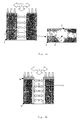
- Fig. 1a is a schematic representation of a single damascene structure wherein the chemicals diffuse into the micropores and react with the low-k material.
- Fig. 1b is a schematic representation of a single damascene structure with top hard mask wherein the chemicals only modify the side walls of the opening.
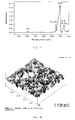
- Fig. 2a shows an FTIR spectrum measured from a 500 nm thick AURORA TM layer.
- Fig. 2b is a 3D Atomic Force Microscopy image showing the surface roughness over an area of 1 x 1 ⁇ m 2 of a 500 nm thick AURORA TM film.
- Fig. 3 represents the toluene adsorption kinetic in AURORA TM.
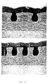
- Fig. 4 represents cross-section SEM pictures of trenches etched in AURORA TM after different strips: (a) high pressure and high temperature O 2 plasma and (b) N 2 /O 2 plasma (low temperature and low pressure).
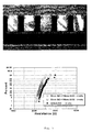
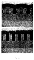
- Fig. 5 shows Focused Ion Beam (FIB) image of 0.25 ⁇ m Cu trenches in AURORA TM made with a double hard mask (50 nm SiC / 150 nm SiO 2 ) (a) , and resistance of 1.8 cm long meanders (0.25 ⁇ m wide) for different strips and hard masks (b). 56 chips per wafer were measured.
- FIB Focused Ion Beam
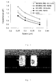
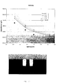
- Fig. 6 is the interline capacitance of AURORA TM trenches as a function of the line spacing for different hard masks and strips.
- Fig. 7 is a cross-section FIB image of a 0.25 ⁇ m interline capacitance structure (100 nm SiC hard mask and O 2 in-situ strip).
- Fig. 8 is a schematic drawing of the dielectric stack used in the etch/strip development and single damascene integration.
- Fig. 9 represents cross-sectional SEM of isolated and dense 0.25 ⁇ m trenches etched on 500 nm Tri-methyl-Silane-03 low-k with 100 nm Buried low-k (BlokTM) hard mask from applied Materials.
- Fig. 10 shows 0.25 ⁇ m isolated and dense trenches after stripping in a high pressure and high temperature oxygen plasma.
- Fig. 11 shows 0.25 ⁇ m isolated and dense trenches after stripping in a O 2 /CF 4 plasma at low temperature and slightly lower pressure than the process of Fig. 11.
- Fig. 12 shows 0.25 ⁇ m isolated and dense trenches after stripping in a H 2 O/CF 4 plasma at low temperature and slightly lower pressure (similar conditions as the process shown in Fig. 11).
- Fig. 13 shows 0.25 ⁇ m isolated and dense trenches after stripping in an O 2 plasma (in-situ) at low temperature and low pressure.
- Fig. 14 shows 0.25 ⁇ m isolated and dense trenches after stripping in a N 2 /O 2 plasma.
- Fig. 15 shows the interline capacitance measured at 100 kHz and simulated for different line spacing after single damascene process, using the water vapour strip process.
- the solid lines represent simulation results with different dielectric constant values.
- Fig. 16 shows the interline capacitance measured at 100 kHz and simulated for different line spacing after single damascene process, using the O 2 in-situ strip process.
- the solid lines represent simulation results with different dielectric constant values.
- Fig. 17 shows the interline capacitance measured at 100 kHz and simulated for different line spacing after single damascene process, using the N 2 /O 2 in-situ strip process.
- the solid lines represent simulation results with different dielectric constant values.
- FIB image of the interline capacitance structure (nominal 0.25/0.25 ⁇ m line/space). Due to the poor contrast between the Pt (FIB preparation) and SiC, the top hard mask cannot be clearly seen in this image.
- Figs. 18 a-d show a process sequence according to a preferred embodiment of the present invention.
- Scaling the dielectric constant is one of the main driving forces for research and development of new back-end-of-line dielectrics.
- the scalability of the k value has become a significant parameter in the selection process of appropriate low-k dielectrics. Investigation of new dielectrics in view of chemical composition, physical structure and related properties of the as-deposited film is only one aspect in research towards successful implementation of low-k dielectrics.
- Fig. 1a A rather direct and practical way to reduce the k-value of the film is the introduction of pores in the dielectric as illustrated in Fig. 1a.
- Etch and strip chemicals 3 penetrate into the low-k material 1. The degree of penetration depends on pore size and properties of the chemical species used.
- Fig. 1b illustrates the case in which the low-k material 1 is covered with a hard mask 4.
- a hard mask 4 During subsequent processing, e.g. during patterning, stripping or cleaning steps, preferably only the side walls of the opening 6 are exposed to the chemicals 3.
- Such patterning or post patterning treatments change the material features at the side walls 5.
- the relative contribution of the side wall material is dominant for narrow spacing and this is exactly the place where lowering of the k-value is most important.
- a method for forming a porous silicon oxide film by exposing a polymer film comprising Si and C to an oxidising plasma.
- the oxidising plasma changes the porosity of the as-deposited uniform layer and hence the dielectric constant of this layer.
- the lateral and/or vertical diffusion of the chemical species is very fast in the micropores 2.
- the reaction with the low-k material itself is slow compared to the diffusion of said chemicals, but this reaction takes place at each pore wall exposed to the chemicals.
- the very small reactions at the pore wall can have a large effect on the overall k-value, while the thickness of the low-k material remains substantially unchanged as illustrated in Fig. 1b the low-k dielectric is only locally exposed to the chemicals.
- the top surface of the low-k dielectric 1 is being subject to chemicals, e.g. a plasma, in fig. 1b, only the side walls 5 of the opening 6 are in direct contact with the chemicals 3 by the top hard mask 3 which is resistant to the chemicals applied.
- This top hard mask layer 4 is known in damascence technology and comprises silicon or nitrides, carbides and oxides, e.g. SiO 2 , Si 3 N 4 , SiC, SiOC.
- the low-k material can be a silicon-oxygen layer.
- silicon-oxygen should be understood as a material being composed of at least Si and O, e.g. but not limited hereto, SiO 2 , or at least Si, C and O, e.g. silicon oxycarbide (SiOC), or at least Si, N, O, and C, e.g. nitrited silicon oxycarbide (SiNOC), or at least Si, C, O and H, e.g. hydrogenated SiOC, or at least Si, O,C, N and H , e.g. hydrogenated SiNOC.
- the low-k material can be a carbide-silicon layer.
- a carbide-silicon layer is an electrically insulating layer being composed of at least Si and C, e.g. SiC, or of at least Si, C and O, e.g.. a silicon oxycarbide (SiOC), or at least Si, C and H as e.g. amorphous hydrogenated silicon carbide SiC:H.
- the preservation of the dielectric constant of a DMS-based low-k dielectric is disclosed.
- the AURORA TM films is deposited in a single-wafer, parallel plate plasma-enhanced- CVD system based on an Eagle-10 system from ASM International, a Netherlands-based company.
- AURORA TM is a trade mark used by ASM to identify the low-k product formed on the Eagle-10 system using dimethyldimethoxysilane (DMS) is used as precursor and He as additive gas. Temperature during deposition was 400 °C.
- the deposited films have a refractive index of 1.41, as measured by spectroscopic ellipsometry.
- FTIR Fourier Transform Infrared Spectroscopy
- a peak around 800 cm -1 is also observed, and it can be assigned to Si-C, Si-CH 2 and Si-CH 3 bonds.
- FTIR spectra measured at centre and edge of the wafer, for both 250 and 500 nm thick AURORA TM films showed the exact same features, indicating a good uniformity in the film structure. No indication of moisture uptake is observed from the FTIR spectrum, even after a month of storage in clean room environment.
- Fig. 2 shows a 3D image of the film surface. An average surface roughness below 0.5 nm is found, and this value is independent of the area measured.
- Fig. 3 shows the kinetic evolution of the adsorptive mass into AURORA TM.
- Toluene which has a molecule kinetic diameter around 0.6 nm, is used as adsorbate vapour.
- the increase of the pressure in the chamber, due to the introduction of toluene vapour, is shown as a function of time. If the film had a pore diameter larger than the kinetic diameter of the toluene molecule, the adsorbate amount in the film would increase in the same rate as the vapour pressure in the chamber.
- Dielectric constant, leakage current and breakdown field were measured using a metal / insulator / metal (MIM) structure, with the top electrode patterned by lithography and dry etch for accurate area determination.
- Capacitance vs. frequency (C-F) measurements were performed. The values reported here were taken at a frequency of 100 kHz.
- Capacitors of different sizes were measured. At least 5 different sites on the wafers were probed. The thickness of the AURORA TM layers used in the calculation of the dielectric constant was measured by spectroscopic ellipsometry. The capacitors measured were located as close as possible to the thickness measurement sites.
- a dielectric constant of 2.9 was found for the AURORA TM films deposited at IMEC.
- the dielectric constant was the same for all the various film thicknesses, and did not change during a period of a month (maximum time interval measured). Annealing the samples at 400°C for 20 minutes did not result in any change of the dielectric constant. A standard deviation of the measurements of around 1% is found, indicating that the dielectric constant does not vary significantly over the wafer.
- Leakage current was measured at a field of 1 MV/cm. The measurements were carried out in a nitrogen environment. The leakage current values are below 10 -11 A/cm 2 and are independent of processing conditions and thickness. The AURORA TM films did not show breakdown up to fields of 2 MV/cm. The measurements were limited to this field by the equipment set-up and film thickness.
- AURORA TM is expected to be sensitive to resist strip processes during patterning of damascene structures, since it involves the use of plasma with oxygen chemistries.
- Single damascene structures using 500 nm AURORA TM with a 100 nm ⁇ -SiC:H (referred as SiC from this point on) etch stop layer were fabricated.
- Two different hard masks were used: 100 nm SiC or a double layer 50 nm SiC / 150 nm SiO 2 .
- Etching of hard mask and AURORA TM was carried out in a LAM 4520XL, a dual frequency reactive ion etch (RIE) system designed for advanced oxide etch applications and offered by LAM, a united States based Company.
- the 100 nm SiC hard mask was etched using an Ar/N 2 /CF 4 /O 2 chemistry, which resulted in good CD-control and etch uniformity. Due to differences in etch rates of oxide and SiC, the same etch time used for etching 100 nm SiC could be used for opening of the double hard mask, with similar characteristics for CD-control and uniformity.
- Etching of the trenches was done using a Ar/CF 4 /CHF 3 /O 2 chemistry, resulting in trenches with straight profiles and no faceting of the hard mask was observed.
- Various stripping processes were evaluated in order to remove the remaining photo resist and polymers formed during the trench etch.
- a downstream O 2 plasma (high temperature, high pressure) and a O 2 /CF 4 plasma (lower pressure and temperature) resulted in undercut and bowing, as can be seen in fig. 4a.
- Fig. 4b shows a cross-section SEM image of AURORA TM trenches after stripping in N 2 /O 2 . No bowing or undercut is present, and some rounding of the hard mask is observed due to this Reactive Ion Etch (RIE)-type strip.
- RIE Reactive Ion Etch
- FIG. 5 shows a cross-section image of 0.25 ⁇ m Cu trenches of a meander/fork structure made in AURORA TM with the 50 nm SiC / 150 nm SiO 2 double hard mask. The resistance of 1.8 cm long meanders is also shown in the figure.
- the metallization scheme consisted of PVD TaN followed by PVD Cu seed layer and subsequent Cu electroplating fill in an ECD chamber from Semitool.
- the wafer with 100 nm SiC hard mask stripped with the O 2 in-situ process shows slightly higher values than the ones with the double hard mask and same strip. The small difference comes from the fact that the total trench depth is smaller (due to the thinner hard mask) and less hard mask is removed during the CMP process when 100 nm SiC is used.
- FIG. 6 shows interline capacitance as a function of various line spacings for wafers with different hard masks and different strip processes.
- Interline capacitance of single damascene oxide structures is plotted for comparison.
- the capacitance of the structures prepared with the double hard mask (SiC/SiO 2 ) is higher than the ones prepared with a single SiC hard mask due to the higher thickness of the trenches ( ⁇ 60 nm thicker). No significant difference is observed between the two different strip splits: O 2 in-situ and N 2 /O 2 .
- the lower k-value found can be due to the modification of the material at the trench side wall, resulting in a less dense film with lower dielectric constant.
- One possible explanation for the lowering of the dielectric constant between lines upon single damascene integration is the formation of a modified material with lower density (more porous), due to the removal of carbon from the film during the strip process.
- TMS-O3 based low-k dielectric was done in a sub-atmospheric chemical vapour deposition (SACVD) CxZ chamber of Applied Materials, a United States-based company.
- SACVD sub-atmospheric chemical vapour deposition
- the film structure is investigated by FTIR and a typical spectrum of the film is given in Fig. 8.
- the main features in this spectrum are the strong absorption peaks due the presence of the Si-O bonds and the presence of C-H and Si-CH 3 bonds.
- the film has a stress value of 6 10 8 dynes/cm 2 (60MPa) and this value is the same after thermal cycling up to 500 °C.
- the film is stable to temperatures up to 550 °C, as found by thermal desorption spectroscopy (TDS) analysis.
- the single-damascene stack consists of (from Si substrate) 50 nm SiN / 500 nm SiO2 / 50 nm BloK / 500 nm TMS-O3 / 100 nm BloK as shown in Fig. 9.
- BloK stands for Buried Low-k material and comprises SiC.
- the etchings have been performed in a LAM 4520 XL tool. Results are presented for tests on patterned wafers. Also, a limited number of strip experiments has been conducted. It is important to mention that the lithography process was target to 0.25 ⁇ m dimensions.
- HM-opening of the 100 nm SiC layer is performed using a slightly modified recipe that is standardly used in oxide damascene etching.
- This Ar/N 2 /CF 4 /O 2 recipe yields very straight (remaining) resist and SiC profiles, and sufficient resist selectivity, as about 250 nm of resist is left in between dense trenches for the standard process.
- the disadvantage however, lies in the side wall roughness which is generated by this process, and which is only visible in top-down inspection.
- Fig. 10 shows cross-section SEM images of isolated and dense 0.25 ⁇ m trenches after etching.
- resist removal process is a critical step in the patterning of Si-O-C type materials, since these films are very sensitive to oxygen plasma processes. Five resist stripping recipes were selected and tested.
- Fig. 13 shows cross section SEM images of isolated and dense trenches after stripping with this process.
- FIG. 14 shows the trenches profiles of the wafer stripped in an O 2 plasma (in-situ) at low pressure and low temperature. Reduced undercut is observed. Generally, the trenches look acceptable except for the fact that the oxide underneath the SiC stopping-layer appears to have been etched for all features. As the etch process applied to this wafer was exactly the same as for the other stripped wafers, this can only be attributed to the stripping method. It is believed that the fluorine which is present in the chamber and on the wafer after the etch could be responsible for this unwanted bottom SiC etch during the resist strip.
- the etching process consisted of a first step using Ar/N 2 /CF 4 /O 2 for hard mask opening followed by Ar/CF 4 /CHF 3 /O 2 for etching of the low-k material.
- Low temperature and low pressure N 2 /O 2 and in-situ O 2 plasma and the "standard" H 2 O-vapour strip processes were used as splits in the wafer processing.
- the metallization scheme consisted of deposition of Physical Vapour Deposition (PVD) TaN barrier followed by PVD Cu seed layer deposition, done in the Applied MATerials Electra-tool. The trenches were then electroplated filled in a Semitool Electro Chemical Deposition (ECD) chamber. Chemical Mechanical Polishing was performed in an IPEC 676 tool. The conditions of these processes were kept constant.
- PVD Physical Vapour Deposition
- ECD Semitool Electro Chemical Deposition
- Interline capacitance structures consisting of long parallel lines with spacing varying from 0.4 down to 0.2 mm were measured. 16 chips per wafer were manually measured (a column from north to south and a row from east to west). After measurements, the wafers were sent for cross-section FIB and later SEM analysis, in order to determine the real profile of the structures (trench and spacing dimensions, hard mask and trench thicknesses) electrically measured. The correct dimensions were used in the simulations performed for estimation of the dielectric constant of the TMS-O3 material after full integration into single damascene structures. The TMA Raphael software package was used in the simulations. Figs. 16 and 17 show the interline capacitance as a function of actual spacing between the lines, as extracted from the FIB and SEM cross-section images.
- the measured value (solid circles) is plotted together with the simulation results for different k values of the low-k material (from 2.2 up to 2.8).
- the dielectric constant values of the other materials used in the simulations were 4.3 for SiO 2 and SiC and 8 for SiN.
- this low dielectric constant value found after single damascene integration can be the fact that the low-k film is modified during the ashing process.
- the film could be converted into a more porous film (or lower density) due to the removal of C from the film in the presence of oxygen during the stripping process.
- a method for sealing the exposed surfaces of a low-k dielectric. In the first and second preferred embodiments this method is applied on two specific examples of low-k dielectrics.
- Figs. 18 a-d illustrate the sequence of creating an opening in a dielectric layer.
- This dielectric layer is part of a damascene dielectric stack.
- the semiconductor substrate 100 is shown.
- This semiconductor substrate can be any substrate used in semiconductor industry such as silicon wafers and can further comprise active devices such as transistors or passive devices such as capacitors and resistors.
- the substrate can further comprise patterned layers of dielectrics and conductive materials to form an interconnect structure.
- a single low-k dielectric layer 11 is shown, but the invention is not limited thereto.
- a top hard mask layer 14 can be formed as is normal practice in damascene back-end-of-line (BEOL) technology.
- the patterning of the dielectric stack in this example the low-k dielectric 11 and the hard mask 14, comprises the steps of depositing and patterning in a lithographic process step a resist layer 21 (Fig. 18a).
- the pattern established in the resist layer 21 is then transferred to the underlying layers, which in this example are the hard mask 14 and the low-k dielectric 11.
- the resist pattern is transferred by creating a dry etch plasma 13 that interacts with the exposed parts of the underlying layers.
- the etch plasma 13 creates an opening 16 in the dielectric stack.
- the etch plasma can create pores 12 or change the porosity of the low-k dielectric layer 11. As explained previously this change in porosity will result in a locally decreased dielectric constant.
- the protective resist layer 21 is removed. The protective resist layer 21 can also be removed during the process of creating the opening 16.
- Fig. 18c shows the device after patterning the opening 16.
- a diffusion barrier layer e.g. nitride or SiC
- a stack of conductive layers e.g. Cu seed layer used for plating Cu on the wafer.
- the dielectric constant can be locally decreased during the step of creating the opening subsequent processing might a negative impact on these local k value.
- the surface of the dielectric layer 11 can be protected by a hard mask 14, the openings 16 formed in the hard mask and in the dielectric layer to receive the barrier and conductive layers make the low-k dielectric susceptible to further processing.
- the negative impact of the cleaning solution that is used can be high. It is to be expected that the problem of cleaning of porous materials will even be much more difficult, but also for the nonporous low-k materials, the danger of low-k material modification in the cleaning step is clear and present. A reason for this degradation might be that the thus created pores 12 are filled with residues or materials during further processing.
- the present invention therefore discloses a method for preserving this local k-value by sealing the exposed surfaces of the porous dielectric layers.
- Fig. 18d shows the sealing of pores 12 created from the side walls 15 of the low-k dielectric 11 onwards.
- the sealing results from the formation of a layer 22 at least on these side walls 15.
- This protective or sealing layer 22 can be formed after the step of patterning the opening 16 and stripping the resist layer 21.
- This protective layer 22 can be formed during the step of creating the opening 16.
- This protective layer 22 can be formed during the step of removing the resist layer 21.
- the protective layer can be formed using a plasma comprising oxygen and nitrogen.
- the dry etch plasma conditions could be for instance :
Landscapes
- Internal Circuitry In Semiconductor Integrated Circuit Devices (AREA)
- Element Separation (AREA)
Applications Claiming Priority (2)
| Application Number | Priority Date | Filing Date | Title |
|---|---|---|---|
| US236569 | 1988-08-25 | ||
| US23656900P | 2000-09-29 | 2000-09-29 |
Publications (3)
| Publication Number | Publication Date |
|---|---|
| EP1195801A2 true EP1195801A2 (de) | 2002-04-10 |
| EP1195801A3 EP1195801A3 (de) | 2009-06-03 |
| EP1195801B1 EP1195801B1 (de) | 2014-01-29 |
Family
ID=22890041
Family Applications (1)
| Application Number | Title | Priority Date | Filing Date |
|---|---|---|---|
| EP01870205.0A Expired - Lifetime EP1195801B1 (de) | 2000-09-29 | 2001-09-28 | Verfahren zur Behandlung einer Isolierschicht mit niedriger Dielektrizitätskonstante |
Country Status (1)
| Country | Link |
|---|---|
| EP (1) | EP1195801B1 (de) |
Cited By (13)
| Publication number | Priority date | Publication date | Assignee | Title |
|---|---|---|---|---|
| WO2003105196A3 (en) * | 2002-06-10 | 2004-03-04 | Intel Corp | Method for controlling etch bias of carbon doped oxide films |
| WO2003107411A3 (en) * | 2002-06-14 | 2004-03-04 | Trikon Technologies Ltd | Porous dielectric films with a non-porous surface |
| US6824699B2 (en) | 1999-02-26 | 2004-11-30 | Trikon Holdings Ltd. | Method of treating an insulting layer |
| US6831003B1 (en) | 2002-05-31 | 2004-12-14 | Advanced Micro Devices, Inc. | Continuous barrier for interconnect structure formed in porous dielectric material with minimized electromigration |
| WO2005062348A1 (de) * | 2003-12-23 | 2005-07-07 | Infineon Technologies Ag | Verfahren zum herstellen eines gridcaps mit lokal erhöhter dielektrischer konstante |
| US6933246B2 (en) | 2002-06-14 | 2005-08-23 | Trikon Technologies Limited | Dielectric film |
| CN100346455C (zh) * | 2004-05-17 | 2007-10-31 | 西安交通大学 | 在腐蚀过程中保护微机械器件金属连线的密封方法 |
| CN100382301C (zh) * | 2003-05-08 | 2008-04-16 | 国际商业机器公司 | 生成多孔有机电介质的方法 |
| DE102007046846A1 (de) * | 2007-09-29 | 2009-04-09 | Advanced Micro Devices, Inc., Sunnyvale | Seitenwandschutzschicht |
| US7875506B2 (en) | 2004-10-13 | 2011-01-25 | Semiconductor Energy Laboratory Co., Ltd. | Etching method and manufacturing method of semiconductor device |
| US8283255B2 (en) | 2007-05-24 | 2012-10-09 | Lam Research Corporation | In-situ photoresist strip during plasma etching of active hard mask |
| JP2020125223A (ja) * | 2019-02-04 | 2020-08-20 | 国立大学法人東海国立大学機構 | 窒化炭素膜の製造方法および窒化炭素被覆体の製造方法 |
| US20230317468A1 (en) * | 2022-03-31 | 2023-10-05 | Nanya Technology Corporation | Reworking process for fabricating semiconductor device |
Family Cites Families (2)
| Publication number | Priority date | Publication date | Assignee | Title |
|---|---|---|---|---|
| US6114250A (en) * | 1998-08-17 | 2000-09-05 | Lam Research Corporation | Techniques for etching a low capacitance dielectric layer on a substrate |
| FR2789804B1 (fr) * | 1999-02-17 | 2002-08-23 | France Telecom | Procede de gravure anisotrope par plasma gazeux d'un materiau polymere dielectrique organique et application a la microelectronique |
-
2001
- 2001-09-28 EP EP01870205.0A patent/EP1195801B1/de not_active Expired - Lifetime
Non-Patent Citations (1)
| Title |
|---|
| None |
Cited By (19)
| Publication number | Priority date | Publication date | Assignee | Title |
|---|---|---|---|---|
| US6824699B2 (en) | 1999-02-26 | 2004-11-30 | Trikon Holdings Ltd. | Method of treating an insulting layer |
| US6831003B1 (en) | 2002-05-31 | 2004-12-14 | Advanced Micro Devices, Inc. | Continuous barrier for interconnect structure formed in porous dielectric material with minimized electromigration |
| CN1302525C (zh) * | 2002-06-10 | 2007-02-28 | 英特尔公司 | 用于控制掺碳氧化物薄膜的蚀刻偏差的方法 |
| WO2003105196A3 (en) * | 2002-06-10 | 2004-03-04 | Intel Corp | Method for controlling etch bias of carbon doped oxide films |
| WO2003107411A3 (en) * | 2002-06-14 | 2004-03-04 | Trikon Technologies Ltd | Porous dielectric films with a non-porous surface |
| GB2410832A (en) * | 2002-06-14 | 2005-08-10 | Trikon Technologies Ltd | Porous dielectric films with a non-porous surface |
| US6933246B2 (en) | 2002-06-14 | 2005-08-23 | Trikon Technologies Limited | Dielectric film |
| CN100382301C (zh) * | 2003-05-08 | 2008-04-16 | 国际商业机器公司 | 生成多孔有机电介质的方法 |
| US7482288B2 (en) | 2003-12-23 | 2009-01-27 | Infineon Technologies Ag | Method for producing a grid cap with a locally increased dielectric constant |
| WO2005062348A1 (de) * | 2003-12-23 | 2005-07-07 | Infineon Technologies Ag | Verfahren zum herstellen eines gridcaps mit lokal erhöhter dielektrischer konstante |
| CN100346455C (zh) * | 2004-05-17 | 2007-10-31 | 西安交通大学 | 在腐蚀过程中保护微机械器件金属连线的密封方法 |
| US7875506B2 (en) | 2004-10-13 | 2011-01-25 | Semiconductor Energy Laboratory Co., Ltd. | Etching method and manufacturing method of semiconductor device |
| US8143168B2 (en) | 2004-10-13 | 2012-03-27 | Semiconductor Energy Laboratory Co., Ltd. | Etching method and manufacturing method of semiconductor device |
| US8283255B2 (en) | 2007-05-24 | 2012-10-09 | Lam Research Corporation | In-situ photoresist strip during plasma etching of active hard mask |
| US8912633B2 (en) | 2007-05-24 | 2014-12-16 | Lam Research Corporation | In-situ photoresist strip during plasma etching of active hard mask |
| DE102007046846A1 (de) * | 2007-09-29 | 2009-04-09 | Advanced Micro Devices, Inc., Sunnyvale | Seitenwandschutzschicht |
| JP2020125223A (ja) * | 2019-02-04 | 2020-08-20 | 国立大学法人東海国立大学機構 | 窒化炭素膜の製造方法および窒化炭素被覆体の製造方法 |
| US20230317468A1 (en) * | 2022-03-31 | 2023-10-05 | Nanya Technology Corporation | Reworking process for fabricating semiconductor device |
| US12293922B2 (en) * | 2022-03-31 | 2025-05-06 | Nanya Technology Corporation | Reworking process of a failed hard mask for fabricating a semiconductor device |
Also Published As
| Publication number | Publication date |
|---|---|
| EP1195801A3 (de) | 2009-06-03 |
| EP1195801B1 (de) | 2014-01-29 |
Similar Documents
| Publication | Publication Date | Title |
|---|---|---|
| US6844266B2 (en) | Anisotropic etching of organic-containing insulating layers | |
| US6168726B1 (en) | Etching an oxidized organo-silane film | |
| KR102625367B1 (ko) | 반도체 구조를 에칭하기 위한 질소-함유 화합물 | |
| EP0826791B1 (de) | Verfahren zum Herstellen eines isolierenden Zwischenfilms | |
| US7052932B2 (en) | Oxygen doped SiC for Cu barrier and etch stop layer in dual damascene fabrication | |
| US7795148B2 (en) | Method for removing damaged dielectric material | |
| US7851384B2 (en) | Method to mitigate impact of UV and E-beam exposure on semiconductor device film properties by use of a bilayer film | |
| US6284644B1 (en) | IMD scheme by post-plasma treatment of FSG and TEOS oxide capping layer | |
| US6573175B1 (en) | Dry low k film application for interlevel dielectric and method of cleaning etched features | |
| KR100887225B1 (ko) | 반도체 디바이스의 제조 방법 | |
| EP1195801B1 (de) | Verfahren zur Behandlung einer Isolierschicht mit niedriger Dielektrizitätskonstante | |
| EP1394286A1 (de) | Vorbehandlung von organischer Schicht für Abscheidung von Atomschichten | |
| Posseme et al. | Etching mechanisms of low-k SiOCH and selectivity to SiCH and SiO 2 in fluorocarbon based plasmas | |
| KR20210068592A (ko) | 붕소-도핑된 비정질 탄소 하드 마스크 및 방법 | |
| EP1923905A2 (de) | Verfahren und Zusammensetzung zur Wiederherstellung von dielektrischen Eigenschaften von porösen Dielektrizitätsmaterialien | |
| Yonekura et al. | Low-damage damascene patterning using porous inorganic low-dielectric-constant materials | |
| Baklanov et al. | Low temperature oxidation and selective etching of chemical vapor deposition a-SiC: H films | |
| US20050077628A1 (en) | Dual damascene structure and method | |
| US20180174897A1 (en) | Method of selective deposition for beol dielectric etch | |
| US7646101B2 (en) | Semiconductor device and manufacturing method thereof | |
| KR20050084286A (ko) | 나이트로겐-비함유 유전성 비반사 코팅부 및 하드마스크 | |
| JPWO2007142172A1 (ja) | 多層配線製造方法と多層配線構造と多層配線製造装置 | |
| Donaton et al. | Characterization and integration in Cu damascene structures of AURORA, an inorganic low-k dielectric | |
| Choi et al. | Characterization and integration of new porous low-k dielectric (k< 2.3) for 65 nm technology and beyond | |
| KR20070042887A (ko) | 피쳐 제한부들을 형성하는 방법 |
Legal Events
| Date | Code | Title | Description |
|---|---|---|---|
| PUAI | Public reference made under article 153(3) epc to a published international application that has entered the european phase |
Free format text: ORIGINAL CODE: 0009012 |
|
| AK | Designated contracting states |
Kind code of ref document: A2 Designated state(s): AT BE CH CY DE DK ES FI FR GB GR IE IT LI LU MC NL PT SE TR |
|
| AX | Request for extension of the european patent |
Free format text: AL;LT;LV;MK;RO;SI |
|
| PUAL | Search report despatched |
Free format text: ORIGINAL CODE: 0009013 |
|
| AK | Designated contracting states |
Kind code of ref document: A3 Designated state(s): AT BE CH CY DE DK ES FI FR GB GR IE IT LI LU MC NL PT SE TR |
|
| AX | Request for extension of the european patent |
Extension state: AL LT LV MK RO SI |
|
| RAP1 | Party data changed (applicant data changed or rights of an application transferred) |
Owner name: IMEC Owner name: APPLIED MATERIALS, INC. |
|
| 17P | Request for examination filed |
Effective date: 20091123 |
|
| AKX | Designation fees paid |
Designated state(s): DE FR GB |
|
| 17Q | First examination report despatched |
Effective date: 20100225 |
|
| GRAP | Despatch of communication of intention to grant a patent |
Free format text: ORIGINAL CODE: EPIDOSNIGR1 |
|
| INTG | Intention to grant announced |
Effective date: 20130822 |
|
| GRAS | Grant fee paid |
Free format text: ORIGINAL CODE: EPIDOSNIGR3 |
|
| GRAA | (expected) grant |
Free format text: ORIGINAL CODE: 0009210 |
|
| AK | Designated contracting states |
Kind code of ref document: B1 Designated state(s): DE FR GB |
|
| REG | Reference to a national code |
Ref country code: GB Ref legal event code: FG4D |
|
| REG | Reference to a national code |
Ref country code: DE Ref legal event code: R096 Ref document number: 60148582 Country of ref document: DE Effective date: 20140306 |
|
| REG | Reference to a national code |
Ref country code: DE Ref legal event code: R097 Ref document number: 60148582 Country of ref document: DE |
|
| PLBE | No opposition filed within time limit |
Free format text: ORIGINAL CODE: 0009261 |
|
| STAA | Information on the status of an ep patent application or granted ep patent |
Free format text: STATUS: NO OPPOSITION FILED WITHIN TIME LIMIT |
|
| 26N | No opposition filed |
Effective date: 20141030 |
|
| REG | Reference to a national code |
Ref country code: DE Ref legal event code: R097 Ref document number: 60148582 Country of ref document: DE Effective date: 20141030 |
|
| REG | Reference to a national code |
Ref country code: FR Ref legal event code: PLFP Year of fee payment: 16 |
|
| PGFP | Annual fee paid to national office [announced via postgrant information from national office to epo] |
Ref country code: GB Payment date: 20160825 Year of fee payment: 16 Ref country code: DE Payment date: 20160823 Year of fee payment: 16 |
|
| PGFP | Annual fee paid to national office [announced via postgrant information from national office to epo] |
Ref country code: FR Payment date: 20160822 Year of fee payment: 16 |
|
| REG | Reference to a national code |
Ref country code: DE Ref legal event code: R119 Ref document number: 60148582 Country of ref document: DE |
|
| GBPC | Gb: european patent ceased through non-payment of renewal fee |
Effective date: 20170928 |
|
| REG | Reference to a national code |
Ref country code: FR Ref legal event code: ST Effective date: 20180531 |
|
| PG25 | Lapsed in a contracting state [announced via postgrant information from national office to epo] |
Ref country code: GB Free format text: LAPSE BECAUSE OF NON-PAYMENT OF DUE FEES Effective date: 20170928 Ref country code: DE Free format text: LAPSE BECAUSE OF NON-PAYMENT OF DUE FEES Effective date: 20180404 |
|
| PG25 | Lapsed in a contracting state [announced via postgrant information from national office to epo] |
Ref country code: FR Free format text: LAPSE BECAUSE OF NON-PAYMENT OF DUE FEES Effective date: 20171002 |