EP1195217A1 - Method of soldering using lead-free solder and bonded article prepared through soldering by the method - Google Patents
Method of soldering using lead-free solder and bonded article prepared through soldering by the method Download PDFInfo
- Publication number
- EP1195217A1 EP1195217A1 EP00935564A EP00935564A EP1195217A1 EP 1195217 A1 EP1195217 A1 EP 1195217A1 EP 00935564 A EP00935564 A EP 00935564A EP 00935564 A EP00935564 A EP 00935564A EP 1195217 A1 EP1195217 A1 EP 1195217A1
- Authority
- EP
- European Patent Office
- Prior art keywords
- lead
- free solder
- soldering
- joining
- ultrasonic vibration
- Prior art date
- Legal status (The legal status is an assumption and is not a legal conclusion. Google has not performed a legal analysis and makes no representation as to the accuracy of the status listed.)
- Granted
Links
Images



Classifications
-
- B—PERFORMING OPERATIONS; TRANSPORTING
- B23—MACHINE TOOLS; METAL-WORKING NOT OTHERWISE PROVIDED FOR
- B23K—SOLDERING OR UNSOLDERING; WELDING; CLADDING OR PLATING BY SOLDERING OR WELDING; CUTTING BY APPLYING HEAT LOCALLY, e.g. FLAME CUTTING; WORKING BY LASER BEAM
- B23K1/00—Soldering, e.g. brazing, or unsoldering
- B23K1/06—Soldering, e.g. brazing, or unsoldering making use of vibrations, e.g. supersonic vibrations
-
- B—PERFORMING OPERATIONS; TRANSPORTING
- B23—MACHINE TOOLS; METAL-WORKING NOT OTHERWISE PROVIDED FOR
- B23K—SOLDERING OR UNSOLDERING; WELDING; CLADDING OR PLATING BY SOLDERING OR WELDING; CUTTING BY APPLYING HEAT LOCALLY, e.g. FLAME CUTTING; WORKING BY LASER BEAM
- B23K1/00—Soldering, e.g. brazing, or unsoldering
- B23K1/20—Preliminary treatment of work or areas to be soldered, e.g. in respect of a galvanic coating
-
- H—ELECTRICITY
- H05—ELECTRIC TECHNIQUES NOT OTHERWISE PROVIDED FOR
- H05K—PRINTED CIRCUITS; CASINGS OR CONSTRUCTIONAL DETAILS OF ELECTRIC APPARATUS; MANUFACTURE OF ASSEMBLAGES OF ELECTRICAL COMPONENTS
- H05K3/00—Apparatus or processes for manufacturing printed circuits
- H05K3/30—Assembling printed circuits with electric components, e.g. with resistors
- H05K3/32—Assembling printed circuits with electric components, e.g. with resistors electrically connecting electric components or wires to printed circuits
- H05K3/34—Assembling printed circuits with electric components, e.g. with resistors electrically connecting electric components or wires to printed circuits by soldering
- H05K3/346—Solder materials or compositions specially adapted therefor
-
- B—PERFORMING OPERATIONS; TRANSPORTING
- B23—MACHINE TOOLS; METAL-WORKING NOT OTHERWISE PROVIDED FOR
- B23K—SOLDERING OR UNSOLDERING; WELDING; CLADDING OR PLATING BY SOLDERING OR WELDING; CUTTING BY APPLYING HEAT LOCALLY, e.g. FLAME CUTTING; WORKING BY LASER BEAM
- B23K2101/00—Articles made by soldering, welding or cutting
- B23K2101/36—Electric or electronic devices
- B23K2101/40—Semiconductor devices
-
- B—PERFORMING OPERATIONS; TRANSPORTING
- B23—MACHINE TOOLS; METAL-WORKING NOT OTHERWISE PROVIDED FOR
- B23K—SOLDERING OR UNSOLDERING; WELDING; CLADDING OR PLATING BY SOLDERING OR WELDING; CUTTING BY APPLYING HEAT LOCALLY, e.g. FLAME CUTTING; WORKING BY LASER BEAM
- B23K2101/00—Articles made by soldering, welding or cutting
- B23K2101/36—Electric or electronic devices
- B23K2101/42—Printed circuits
-
- B—PERFORMING OPERATIONS; TRANSPORTING
- B23—MACHINE TOOLS; METAL-WORKING NOT OTHERWISE PROVIDED FOR
- B23K—SOLDERING OR UNSOLDERING; WELDING; CLADDING OR PLATING BY SOLDERING OR WELDING; CUTTING BY APPLYING HEAT LOCALLY, e.g. FLAME CUTTING; WORKING BY LASER BEAM
- B23K35/00—Rods, electrodes, materials, or media, for use in soldering, welding, or cutting
- B23K35/22—Rods, electrodes, materials, or media, for use in soldering, welding, or cutting characterised by the composition or nature of the material
- B23K35/24—Selection of soldering or welding materials proper
- B23K35/26—Selection of soldering or welding materials proper with the principal constituent melting at less than 400°C
- B23K35/262—Sn as the principal constituent
Definitions
- the present invention relates to a soldering method using a solder with no lead contained, that is, a lead-free solder, and a joined object soldered with the use of the soldering method.
- solders not containing the lead namely, lead-free solders have been under development lately.
- the lead-free solders based on Sn-Cu (tin-copper), Sn-Ag (tin-silver), Sn-Zn (tin-zinc), Sn-Bi (tin-bismuth), Sn-In (tin-indium), In-Ag (indium-silver), etc. have been developed, and particularly the Sn-Cu based, Sn-Ag based and Sn-Zn based types have potentialities.
- a lead-free solder of a composition for example, of Sn-0.7Cu in the Sn-Cu has a melting point of 227°C
- the Sn-Ag based lead-free solder in a composition of, e.g., Sn-3.5Ag has a melting point of 221°C
- the Sn-Zn based lead-free solder of a composition of, e.g., Sn-8Zn has a melting point of 199°C.
- the melting point of the Sn-Zn based type is lowest among these solders, since Zn is easy to oxidize and no effective means is found at present for preventing the oxidation, the Sn-Zn based lead-free solder involves problems to be solved before used to fix electronic components onto a printed board as described hereinabove. Under the circumstances, the potential lead-free solder now is the Sn-Cu based type and the Sn-Ag based type, but both of which have higher melting points by approximately 40°C than that of the eutectic solder.
- a heat resistant temperature of general electronic components is approximately 230°C. Therefore, a thermal allowance of approximately 50°C is provided when the conventional eutectic solder is used to fix electronic components onto the printed board. However, the thermal allowance almost disappears in using, e.g., the Sn-Cu based and Sn-Ag based lead-free solders for the fixing. The thermal allowance is still more extreme for components weakly resistant to heat such as, for instance, aluminum electrolytic capacitors and the like.
- lead-free solders for decreasing the melting points of the lead-free solders to or lower than the melting point of the conventional eutectic solder as much as possible, there is proposed lead-free solders in composition of, e.g., Sn-3.5Ag-6Bi, Sn-3.5Ag-3Bi-3In and the like having Bi (bismuth), In (indium) and the like added as a melting point decrease action metal acting to decrease the melting point.
- the conventional eutectic solder changes almost instantaneously from a melt state to a solid state.
- the melting point of the lead-free solder decreases in proportion to an added amount of Bi when the Bi is added to the lead-free solder.
- a temperature range in which the lead-free solder changes from a melt state to a solid state expands as compared with that of the conventional eutectic solder.
- the lead-free solder is brought into a state in which a partially solidified part and a part still in the melt state mix.
- crystals of, e.g., Bi growing large in the lead-free solder 4 may segregation at a joining part 3 between an electronic component 1 and an electrode 2 of a printed board 5 as shown in Fig. 8.
- An enlarged illustration of the joining part in Fig. 8 diagrammatically shows a composition of the lead-free solder 4 at the joining part 3, in which a symbol " ⁇ " corresponds to, e.g., Bi and a symbol " ⁇ " corresponds to, e.g., Ag.
- a symbol " ⁇ " shown at a joining interfacial part to the electrode 2 corresponds to a compound of Cu as a material of the electrode 2 and Sn in the lead-free solder.
- Bi itself has a higher hardness than hardnesses of Sn and Ag. Therefore a strength of the lead-free solder at a part where Bi gathers due to the segregation of Bi crystals becomes brittle when the Bi is included by, e.g., several tens wt.% in the lead-free solder.
- a joining strength at the joining interfacial part decreases if the Bi crystals are unevenly distributed and then solidified at the joining interfacial part of the electrode 2, leading to the trouble that a sufficient joining strength cannot be obtained between the electrode 2 and the electronic component 1.
- a content of Bi at present is hence unavoidably limited to several wt.% from a view point of a reliability on the joining strength, and therefore the melting point cannot be sufficiently lowered at present.
- the melting point of the present lead-free solder is higher than the melting point of the eutectic solder as depicted above, for example, a larger power is inevitably required for melting the solder than when the eutectic solder is used, thereby raising problems in view of costs and saving energy. Further components of a low thermal resistance cannot be soldered with the use of the lead-free solder.
- the present invention is devised to solve the above-described problems and has for its object to provide a method of soldering a lead-free solder which lowers a melting point of the lead-free solder and prevents deterioration of a joining strength at parts joined by the lead-free solder, and joined objects soldered with the use of the soldering method.
- a method of soldering a lead-free solder which comprises:
- the ultrasonic vibration can be such that makes crystals of components contained in the lead-free solder fine and prevents segregation of the contained components, and increases the joining strength between the mount article and the member to be mounted.
- the ultrasonic vibration may be such that makes crystals of components contained in the lead-free solder fine and prevents segregation of the contained components at a joining interface of at least either the mount article or the member to be mounted, and increases the joining strength between the mount article and the member to be mounted at the joining interface.
- the contained components may include a component of a melting point decrease action metal for acting to decrease a melting point of the lead-free solder.
- the ultrasonic vibration may be such that increases a thickness of a layer of a compound of Sn included in the lead-free solder and the Cu, the compound existing at the joining interface, and increases the joining strength between the mount article and the member to be mounted at the joining interface.
- the lead-free solder may have a Sn-Ag based composition as a main ingredient.
- the above-mentioned contained components may include an alloy component of the Sn-Ag.
- the melting point decrease action metal can be at least one of Bi, Cu, Zn and In.
- a joined object according to a second aspect of the present invention is soldered with the use of the method of soldering the lead-free solder of the first aspect.
- the soldering method of the lead-free solder in the first aspect of the present invention since the ultrasonic vibration is let to act when the molten lead-free solder is solidified, crystals of the components contained in the lead-free solder can be turned minute and prevented from segregating at the joining interface of at least one of the mount article and the member to be mounted which are to be joined by the lead-free solder, so that the joining strength between the mount article and the member to be mounted at the joining interface can be increased as compared with a case without the ultrasonic vibration acted.
- a printed board and an electronic component are given as examples of the joined object in the case where the electronic component as an example of a mount article is to be soldered onto the printed board as an example of a member to be mounted.
- solder which is an alloy of tin with no lead contained, i.e., a lead-free solder
- a lead-free solder in which Bi as a metal acting to lower a melting point of the lead-free solder, that is, Bi as a melting point decrease action metal is added to the above Sn-Ag based solder is taken.
- the lead-free solder is not limited to this composition and can be the earlier-described Sn-Cu based type, Sn-Zn based type, Sn-Bi based type, Sn-In based type, In-Ag based type or the like
- the melting point decrease action metal to be added can be Bi, In, Cu or the like.
- the melting point decrease action metal exceeds by approximately 0.5wt.%, is not limited to a single composition of, for instance, Bi or the like and may have an alloy containing, e.g., Bi or the like.
- a lead-free solder 101 used in the soldering method has a composition of Sn-Ag-Bi.
- a content of Bi is set to be 20wt.% and 40wt. %.
- a maximum value of the content of Bi is 58wt.% (Sn-58Bi) where Bi is turned to a eutectic state to Sn without Ag included.
- step (designated by "S" in the drawing) the lead-free solder 101 in the composition of, for example, Sn-3.5Ag-40Bi is melted.
- step 2 for the earlier referred electronic component 1 and printed board 5 constituting the joined object, the lead-free solder 101 is brought in contact with a part 3 to be joined between the electronic component 1 and an electrode 2 on the printed board 5.
- next step 3 the lead-free solder 101 including the joined portion 3 is started to be cooled. Further, an ultrasonic horn of an ultrasonic oscillator is brought into contact with the printed board 5 so as to generate a vibration to at least the joined portion 3.
- the vibration has a frequency of a level at which crystals are made fine and prevented from being unevenly distributed as will be described later, that is, for example, an amplitude of several ⁇ m.
- the lead-free solder 101 is vibrated by the ultrasonic vibration when the ultrasonic vibration is acted to the joined portion 3.
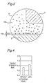
- Overgrown Bi crystals 31 as shown in Fig. 8 are turned fine as indicated in Fig. 3 owing to the action of the vibration and moreover the lead-free solder 101 is blended by the action of the vibration, so that Bi crystals can be prevented from being unevenly distributed, for instance, to a joining interface of the electrode 2.
- crystals of Bi having a higher hardness than hardnesses of the other components in the lead-free solder 101 e.g., Sn, Ag or the like are prevented from being segregated and solidified in a state that the crystals of Bi are gathered to, for example, the joining interface of the electrode 2.
- the ultrasonic vibration works to make fine crystals of this Sn-Ag alloy as well.
- the whole of the joined portion 3 is hence made nearly uniform in composition and moreover, crystals in each composition are made fine. Accordingly, a strength of the entire joined portion 3 is unified and the joining strength at the joining interface of the electrode 2 can be enhanced in comparison with the conventional art without the ultrasonic vibration acted.
- Effects as follows can be further obtained by acting the ultrasonic vibration. Specifically, although a compound of Sn and Cu included in the lead-free solder 101 is formed to surface portions of the electrode 2 and an electrode of the electronic component 1 having Cu as a main ingredient as described above, a layer including the Sn-Cu compound is diffused to grow in the lead-free solder 101 by the ultrasonic vibration when the vibration is acted.
- the joining strength at the joining interface of the electrode 2 can be enhanced more by acting the ultrasonic vibration so that a thickness 102 of the layer including the Sn-Cu compound becomes an appropriate value. The joining strength is reversely weakened if the thickness 102 exceeds the appropriate value, and therefore the frequency and the ultrasonic vibration should be controlled.
- a surface tension of the lead-free solder can be reduced by applying the ultrasonic vibration, a solderability can be improved and the joining strength can be enhanced.
- the amplitude value and the frequency at the joined portion 3 by the ultrasonic vibration are set to such values that components included in the lead-free solder, for example, Bi crystals as mentioned above are made fine at the joining interface of the joined object, crystals of the formed alloy such as Sn-Ag or the like are made fine, the contained components and the alloy crystals are prevented from segregating, and the joining strength of the electrode 2 of the printed board 5 and the electrode of the electronic component 1 at the joining interface is increased, and furthermore, the thickness of the layer including the Sn-Cu compound present at the joining interface is increased, thereby increasing the joining strength at the joining interface and also increasing the solderability.
- Bi crystals as mentioned above are made fine at the joining interface of the joined object
- crystals of the formed alloy such as Sn-Ag or the like are made fine
- the contained components and the alloy crystals are prevented from segregating
- the joining strength of the electrode 2 of the printed board 5 and the electrode of the electronic component 1 at the joining interface is increased, and furthermore, the thickness of the
- the ultrasonic vibration may be started to act concurrently with a time when the molten lead-free solder 101 is started to be cooled, as designated by a time t1 in Fig. 2 or may be started prior to the start of the cooling as indicated by a time t0.
- the action should be started at least immediately before a temperature of the lead-free solder reaches a solidifying temperature of the lead-free solder 101, as indicated by a time t2.
- An end time point of the action of the ultrasonic vibration is after the lead-free solder 101 is perfectly solidified.
- the vibration may be acted intermittently.
- Fig. 4 indicates the experiment result in the case of using the lead-free solder of a composition of Sn-3.5Ag-40Bi
- Fig. 5 shows the experiment result in the case of Sn-3.5Ag-20Bi
- Fig. 6 shows the experiment result in the case of Sn-3.5Ag-6Bi.
- the lead-free solder of the composition of Sn-3.5Ag-40Bi has a melting point of approximately 180°C
- the lead-free solder of the composition of Sn-3.5Ag-20Bi has a melting point of approximately 200°C
- the lead-free solder of the composition of Sn-3.5Ag-6Bi has a melting pointof approximately 216°C.
- a reliability can be obtained even in the lead-free solder with a larger content of Bi than in the conventional art owing to the action of the ultrasonic vibration as above.
- the lead-free solder of a lower melting point than that of the conventional lead-free solder becomes utilizable, enabling, for example, components of the weak heat resistance to be fixed to the printed board or the like by the lead-free solder.
- the power necessary for melting the lead-free solder can be lowered than for the conventional lead-free solder, which is effective to save energy and eventually contributes to protect the environment.
Landscapes
- Engineering & Computer Science (AREA)
- Mechanical Engineering (AREA)
- Manufacturing & Machinery (AREA)
- Microelectronics & Electronic Packaging (AREA)
- Electric Connection Of Electric Components To Printed Circuits (AREA)
Abstract
Description
Claims (20)
- A method of soldering a lead-free solder which comprises:melting the lead-free solder (101) which is an alloy of tin with no lead contained; andacting ultrasonic vibration for increasing a joining strength between a mount article (1) and a member (5) to be mounted to at least one of the mount article and the member to be mounted which are to be joined by the lead-free solder, and the lead-free solder when solidifying the molten lead-free solder.
- The method of soldering the lead-free solder according to claim 1, wherein the ultrasonic vibration is such that makes crystals of components contained in the lead-free solder fine and prevents segregation of the contained components, and increases the joining strength between the mount article and the member to be mounted.
- The method of soldering the lead-free solder according to claim 1, wherein the ultrasonic vibration is such that makes crystals of components contained in the lead-free solder fine and prevents segregation of the contained components at a joining interface of at least one of the mount article and the member to be mounted, and increases the joining strength between the mount article and the member to be mounted at the joining interface.
- The method of soldering the lead-free solder according to claim 2, wherein the ultrasonic vibration is such that makes fine crystals of components contained in the lead-free solder and prevents segregation of the contained components at a joining interface of at least one of the mount article and the member to be mounted, and increases the joining strength between the mount article and the member to be mounted at the joining interface.
- The method of soldering the lead-free solder according to claim 2, wherein the contained components include a component of a melting point decrease action metal for acting to decrease a melting point the lead-free solder.
- The method of soldering the lead-free solder according to claim 3, wherein the contained components include a component of a melting point decrease action metal for acting to decrease a melting point of the lead-free solder.
- The method of soldering the lead-free solder according to claim 4, wherein the contained components include a component of a melting point decrease action metal for acting to decrease a melting point of the lead-free solder.
- The method of soldering the lead-free solder according to claim 3, wherein, when the mount article and the member to be mounted contain Cu, the ultrasonic vibration is such that increases a thickness of a layer of a compound of Sn included in the lead-free solder and the Cu, the compound existing at the joining interface, and increases the joining strength between the mount article and the member to be mounted at the joining interface.
- The method of soldering the lead-free solder according to claim 4, wherein, when the mount article and the member to be mounted contain Cu, the ultrasonic vibration is such that increases a thickness of a layer of a compound of Sn included in the lead-free solder and the Cu, the compound existing at the joining interface, and increases the joining strength between the mount article and the member to be mounted at the joining interface.
- The method of soldering the lead-free solder according to claim 5, wherein, when the mount article and the member to be mounted contain Cu, the ultrasonic vibration is such that increases a thickness of a layer of a compound of Sn included in the lead-free solder and the Cu, the compound existing at the joining interface, and increases the joining strength between the mount article and the member to be mounted at the joining interface.
- The method of soldering the lead-free solder according to claim 6, wherein, when the mount article and the member to be mounted contain Cu, the ultrasonic vibration is such that increases a thickness of a layer of a compound of Sn included in the lead-free solder and the Cu, the compound existing at the joining interface, and increases the joining strength between the mount article and the member to be mounted at the joining interface.
- The method of soldering the lead-free solder according to claim 7, wherein, when the mount article and the member to be mounted contain Cu, the ultrasonic vibration is such that increases a thickness of a layer of a compound of Sn included in the lead-free solder and the Cu, the compound existing at the joining interface, and increases the joining strength between the mount article and the member to be mounted at the joining interface.
- The method of soldering the lead-free solder according to claim 1, wherein the lead-free solder has a Sn-Ag based composition as a main ingredient.
- The method of soldering the lead-free solder according to claim 12, wherein the lead-free solder has a Sn-Ag based composition as a main ingredient.
- The method of soldering the lead-free solder according to claim 13, wherein the contained components include an alloy component of the Sn-Ag.
- The method of soldering the lead-free solder according to claim 14, wherein the contained components include an alloy component of the Sn-Ag.
- The method of soldering the lead-free solder according to claim 5, wherein the melting point decrease action metal is at least one of Bi, Cu, Zn and In.
- The method of soldering the lead-free solder according to claim 8, wherein the melting point decrease action metal is at least one of Bi, Cu, Zn and In.
- The method of soldering the lead-free solder according to claim 13, wherein the melting point decrease action metal is at least one of Bi, Cu, Zn and In.
- A Joined object soldered with the use of the method of soldering the lead-free solder according to any one of claims 1-19.
Applications Claiming Priority (3)
| Application Number | Priority Date | Filing Date | Title |
|---|---|---|---|
| JP16516599 | 1999-06-11 | ||
| JP16516599A JP3580731B2 (en) | 1999-06-11 | 1999-06-11 | Lead-free solder soldering method and joined body soldered by the soldering method |
| PCT/JP2000/003678 WO2000076708A1 (en) | 1999-06-11 | 2000-06-07 | Method of soldering using lead-free solder and bonded article prepared through soldering by the method |
Publications (3)
| Publication Number | Publication Date |
|---|---|
| EP1195217A1 true EP1195217A1 (en) | 2002-04-10 |
| EP1195217A4 EP1195217A4 (en) | 2003-07-23 |
| EP1195217B1 EP1195217B1 (en) | 2004-12-01 |
Family
ID=15807104
Family Applications (1)
| Application Number | Title | Priority Date | Filing Date |
|---|---|---|---|
| EP00935564A Expired - Lifetime EP1195217B1 (en) | 1999-06-11 | 2000-06-07 | Method of soldering using lead-free solder |
Country Status (5)
| Country | Link |
|---|---|
| US (2) | US6702175B1 (en) |
| EP (1) | EP1195217B1 (en) |
| JP (1) | JP3580731B2 (en) |
| DE (1) | DE60016413T2 (en) |
| WO (1) | WO2000076708A1 (en) |
Cited By (4)
| Publication number | Priority date | Publication date | Assignee | Title |
|---|---|---|---|---|
| US6702175B1 (en) * | 1999-06-11 | 2004-03-09 | Matsushita Electric Industrial Co., Ltd. | Method of soldering using lead-free solder and bonded article prepared through soldering by the method |
| EP1488880A3 (en) * | 2003-06-13 | 2006-04-05 | Matsushita Electric Industrial Co., Ltd. | Solder joint structure, soldering method, and electronic-component manufacturing apparatus using the same structure and the method |
| WO2008014900A1 (en) * | 2006-07-31 | 2008-02-07 | FNE Forschungsinstitut für Nichteisen-Metalle GmbH | Method for fitting a connecting conductor to a photovoltaic solar cell |
| EP2359973A3 (en) * | 2010-02-23 | 2012-11-14 | SCHOTT Solar AG | Method and device for applying solder to a workpiece |
Families Citing this family (5)
| Publication number | Priority date | Publication date | Assignee | Title |
|---|---|---|---|---|
| US20040155097A1 (en) * | 2003-02-04 | 2004-08-12 | Matsushita Electric Industrial Co., Ltd. | Soldering method and method for manufacturing component mounting board |
| US7287685B2 (en) * | 2004-09-20 | 2007-10-30 | International Business Machines Corporation | Structure and method to gain substantial reliability improvements in lead-free BGAs assembled with lead-bearing solders |
| US8220697B2 (en) * | 2005-01-18 | 2012-07-17 | Siemens Energy, Inc. | Weldability of alloys with directionally-solidified grain structure |
| JP2010142848A (en) * | 2008-12-19 | 2010-07-01 | Ijr:Kk | Brazing method and brazing apparatus |
| US20120000964A1 (en) * | 2010-07-01 | 2012-01-05 | Gm Global Technology Operations, Inc. | Battery tab joints and methods of making |
Family Cites Families (25)
| Publication number | Priority date | Publication date | Assignee | Title |
|---|---|---|---|---|
| JPS55136562A (en) * | 1979-04-09 | 1980-10-24 | Hitachi Ltd | Ultrasonic pre-soldering method and apparatus thereof |
| DE3240540A1 (en) * | 1982-11-03 | 1984-06-14 | GeWerTec Gesellschaft für Werkstofftechnik mbH, 4600 Dortmund | Method and apparatus for high-temperature soldering and brazing |
| JPS6437077A (en) | 1987-08-03 | 1989-02-07 | Hitachi Ltd | Reflow soldering |
| US4885841A (en) | 1989-02-21 | 1989-12-12 | Micron Technology, Inc. | Vibrational method of aligning the leads of surface-mount electronic components with the mounting pads of printed circuit boards during the molten solder mounting process |
| US5094700A (en) * | 1990-03-22 | 1992-03-10 | University Of Cincinnati | Solder and brazing alloys having improved properties and method of preparation |
| US5256370B1 (en) * | 1992-05-04 | 1996-09-03 | Indium Corp America | Lead-free alloy containing tin silver and indium |
| JPH067926A (en) | 1992-06-10 | 1994-01-18 | Showa Alum Corp | Method for joining aluminum material |
| JPH06342976A (en) * | 1993-06-01 | 1994-12-13 | Nippondenso Co Ltd | Board connection method |
| US5492263A (en) * | 1994-05-26 | 1996-02-20 | Delco Electronics Corp. | Method for wire bonding an aluminum wire to a lead of an electronics package |
| JP2843814B2 (en) | 1994-12-14 | 1999-01-06 | 株式会社アルテクス | Ultrasonic soldering method |
| JP3347512B2 (en) | 1995-03-17 | 2002-11-20 | 富士通株式会社 | Solder alloy for low-temperature bonding, electronic device using the same, and method of manufacturing the same |
| JP3220635B2 (en) | 1996-02-09 | 2001-10-22 | 松下電器産業株式会社 | Solder alloy and cream solder |
| US5730932A (en) * | 1996-03-06 | 1998-03-24 | International Business Machines Corporation | Lead-free, tin-based multi-component solder alloys |
| JP3963501B2 (en) * | 1996-06-12 | 2007-08-22 | 内橋エステック株式会社 | Electronic component mounting method |
| JPH10216630A (en) | 1997-01-31 | 1998-08-18 | Shibaura Eng Works Co Ltd | Ultrasonic vibrator soldering method and ultrasonic vibrator |
| JP3688429B2 (en) * | 1997-04-25 | 2005-08-31 | 株式会社東芝 | Electronic component mounting substrate and electronic component mounting substrate |
| JP3592486B2 (en) | 1997-06-18 | 2004-11-24 | 株式会社東芝 | Soldering equipment |
| US6047876A (en) * | 1997-09-12 | 2000-04-11 | Materials Resources International | Process of using an active solder alloy |
| JPH11330134A (en) * | 1998-05-12 | 1999-11-30 | Hitachi Ltd | Wire bonding method and apparatus, and semiconductor device |
| US6171415B1 (en) * | 1998-09-03 | 2001-01-09 | Uit, Llc | Ultrasonic impact methods for treatment of welded structures |
| JP3580731B2 (en) * | 1999-06-11 | 2004-10-27 | 和美 松重 | Lead-free solder soldering method and joined body soldered by the soldering method |
| CN1144649C (en) * | 1999-06-11 | 2004-04-07 | 日本板硝子株式会社 | Lead-free Solder |
| JP2001230272A (en) * | 2000-02-21 | 2001-08-24 | Nippon Avionics Co Ltd | Flip chip with lead-free solder multilayer bump and lead-free flip chip assembly |
| JP2002076590A (en) * | 2000-08-29 | 2002-03-15 | Matsushita Electric Ind Co Ltd | Component mounting device, component mounting method, component mounting system, and circuit board |
| TW490821B (en) * | 2000-11-16 | 2002-06-11 | Orient Semiconductor Elect Ltd | Application of wire bonding technique on manufacture of wafer bump and wafer level chip scale package |
-
1999
- 1999-06-11 JP JP16516599A patent/JP3580731B2/en not_active Expired - Fee Related
-
2000
- 2000-06-07 US US10/009,168 patent/US6702175B1/en not_active Expired - Fee Related
- 2000-06-07 WO PCT/JP2000/003678 patent/WO2000076708A1/en not_active Ceased
- 2000-06-07 EP EP00935564A patent/EP1195217B1/en not_active Expired - Lifetime
- 2000-06-07 DE DE60016413T patent/DE60016413T2/en not_active Expired - Lifetime
-
2004
- 2004-01-20 US US10/759,191 patent/US20040144829A1/en not_active Abandoned
Cited By (5)
| Publication number | Priority date | Publication date | Assignee | Title |
|---|---|---|---|---|
| US6702175B1 (en) * | 1999-06-11 | 2004-03-09 | Matsushita Electric Industrial Co., Ltd. | Method of soldering using lead-free solder and bonded article prepared through soldering by the method |
| EP1488880A3 (en) * | 2003-06-13 | 2006-04-05 | Matsushita Electric Industrial Co., Ltd. | Solder joint structure, soldering method, and electronic-component manufacturing apparatus using the same structure and the method |
| US7293692B2 (en) | 2003-06-13 | 2007-11-13 | Matsushita Electric Industrial Co., Ltd. | Solder joint structure, soldering method, and electronic-component manufacturing apparatus using the same structure and the method |
| WO2008014900A1 (en) * | 2006-07-31 | 2008-02-07 | FNE Forschungsinstitut für Nichteisen-Metalle GmbH | Method for fitting a connecting conductor to a photovoltaic solar cell |
| EP2359973A3 (en) * | 2010-02-23 | 2012-11-14 | SCHOTT Solar AG | Method and device for applying solder to a workpiece |
Also Published As
| Publication number | Publication date |
|---|---|
| EP1195217A4 (en) | 2003-07-23 |
| DE60016413D1 (en) | 2005-01-05 |
| EP1195217B1 (en) | 2004-12-01 |
| JP3580731B2 (en) | 2004-10-27 |
| WO2000076708A1 (en) | 2000-12-21 |
| US20040144829A1 (en) | 2004-07-29 |
| US6702175B1 (en) | 2004-03-09 |
| DE60016413T2 (en) | 2005-11-03 |
| JP2000351065A (en) | 2000-12-19 |
Similar Documents
| Publication | Publication Date | Title |
|---|---|---|
| US5389160A (en) | Tin bismuth solder paste, and method using paste to form connection having improved high temperature properties | |
| EP0855242B1 (en) | Lead-free solder | |
| EP1614500A1 (en) | Solder paste and printed board | |
| US5229070A (en) | Low temperature-wetting tin-base solder paste | |
| JP4438974B2 (en) | Solder paste | |
| EP0787559B1 (en) | Soldering alloy, cream solder and soldering method | |
| WO2006126564A1 (en) | Lead-free solder paste | |
| JP2001058286A (en) | Solder paste for joining chip parts | |
| WO2007125861A1 (en) | Solder paste | |
| JP2003170294A (en) | Solder paste | |
| JP4401671B2 (en) | High temperature lead-free solder alloys and electronic components | |
| JP2002018589A (en) | Lead-free solder alloy | |
| JP3879582B2 (en) | Solder paste, electronic component and step soldering method | |
| US6702175B1 (en) | Method of soldering using lead-free solder and bonded article prepared through soldering by the method | |
| JP3299091B2 (en) | Lead-free solder alloy | |
| JP3878978B2 (en) | Lead-free solder and lead-free fittings | |
| EP1557235A1 (en) | Lead-free solder and soldered article | |
| JP2001259884A (en) | Paste solder | |
| JP4396162B2 (en) | Lead-free solder paste | |
| Frear | Trends and issues in Pb-free soldering for electronic packaging | |
| JPH09277082A (en) | Solder paste | |
| JP4392020B2 (en) | Lead-free solder balls | |
| JPH1052791A (en) | Lead-free solder alloy | |
| JP4151409B2 (en) | Soldering method | |
| JP2003266193A (en) | Lead-free solder for solder bath supply |
Legal Events
| Date | Code | Title | Description |
|---|---|---|---|
| PUAI | Public reference made under article 153(3) epc to a published international application that has entered the european phase |
Free format text: ORIGINAL CODE: 0009012 |
|
| 17P | Request for examination filed |
Effective date: 20020111 |
|
| AK | Designated contracting states |
Kind code of ref document: A1 Designated state(s): AT BE CH CY DE DK ES FI FR GB GR IE IT LI LU MC NL PT SE |
|
| AX | Request for extension of the european patent |
Free format text: AL;LT;LV;MK;RO;SI |
|
| A4 | Supplementary search report drawn up and despatched |
Effective date: 20030610 |
|
| RIC1 | Information provided on ipc code assigned before grant |
Ipc: 7B 23K 20/10 B Ipc: 7B 23K 1/06 A Ipc: 7B 23K 35/26 B Ipc: 7H 01L 21/607 B Ipc: 7H 05K 3/34 B Ipc: 7B 23K 1/00 B |
|
| 17Q | First examination report despatched |
Effective date: 20031215 |
|
| RBV | Designated contracting states (corrected) |
Designated state(s): DE GB |
|
| GRAP | Despatch of communication of intention to grant a patent |
Free format text: ORIGINAL CODE: EPIDOSNIGR1 |
|
| RTI1 | Title (correction) |
Free format text: METHOD OF SOLDERING USING LEAD-FREE SOLDER |
|
| GRAS | Grant fee paid |
Free format text: ORIGINAL CODE: EPIDOSNIGR3 |
|
| RAP1 | Party data changed (applicant data changed or rights of an application transferred) |
Owner name: MATSUSHITA ELECTRIC INDUSTRIAL CO., LTD. Owner name: MATSUSHIGE, KAZUMI |
|
| RIN1 | Information on inventor provided before grant (corrected) |
Inventor name: MATSUSHIGE, KAZUMI Inventor name: HIBINO, SHUNJI Inventor name: SUETSUGU, KENICHIRO Inventor name: YAMAGUCHI, ATSUSHI Inventor name: HORIUCHI, TOSHIHISA724, MOMOYAMAHIGASHI Inventor name: HIRANO, MASATO Inventor name: IKARI, TAKASHI |
|
| GRAA | (expected) grant |
Free format text: ORIGINAL CODE: 0009210 |
|
| RIN1 | Information on inventor provided before grant (corrected) |
Inventor name: HORIUCHI, TOSHIHISA Inventor name: HIBINO, SHUNJI Inventor name: HIRANO, MASATO Inventor name: IKARI, TAKASHI Inventor name: SUETSUGU, KENICHIRO Inventor name: MATSUSHIGE, KAZUMI Inventor name: YAMAGUCHI, ATSUSHI |
|
| AK | Designated contracting states |
Kind code of ref document: B1 Designated state(s): DE GB |
|
| REG | Reference to a national code |
Ref country code: GB Ref legal event code: FG4D |
|
| RIN2 | Information on inventor provided after grant (corrected) |
Inventor name: HIRANO, MASATO Inventor name: SUETSUGU, KENICHIRO Inventor name: MATSUSHIGE, KAZUMI Inventor name: YAMAGUCHI, ATSUSHI Inventor name: HIBINO, SHUNJI Inventor name: HORIUCHI, TOSHIHISA Inventor name: IKARI, TAKASHI |
|
| REG | Reference to a national code |
Ref country code: IE Ref legal event code: FG4D |
|
| REF | Corresponds to: |
Ref document number: 60016413 Country of ref document: DE Date of ref document: 20050105 Kind code of ref document: P |
|
| PLBE | No opposition filed within time limit |
Free format text: ORIGINAL CODE: 0009261 |
|
| STAA | Information on the status of an ep patent application or granted ep patent |
Free format text: STATUS: NO OPPOSITION FILED WITHIN TIME LIMIT |
|
| 26N | No opposition filed |
Effective date: 20050902 |
|
| PGFP | Annual fee paid to national office [announced via postgrant information from national office to epo] |
Ref country code: GB Payment date: 20110601 Year of fee payment: 12 |
|
| PGFP | Annual fee paid to national office [announced via postgrant information from national office to epo] |
Ref country code: DE Payment date: 20110601 Year of fee payment: 12 |
|
| GBPC | Gb: european patent ceased through non-payment of renewal fee |
Effective date: 20120607 |
|
| REG | Reference to a national code |
Ref country code: DE Ref legal event code: R119 Ref document number: 60016413 Country of ref document: DE Effective date: 20130101 |
|
| PG25 | Lapsed in a contracting state [announced via postgrant information from national office to epo] |
Ref country code: DE Free format text: LAPSE BECAUSE OF NON-PAYMENT OF DUE FEES Effective date: 20130101 Ref country code: GB Free format text: LAPSE BECAUSE OF NON-PAYMENT OF DUE FEES Effective date: 20120607 |